
 Open Access Article
 This Open Access Article is licensed under a Creative Commons Attribution-Non Commercial 3.0 Unported Licence
Controlling the concentration gradient in sequentially deposited bilayer organic solar cells via rubbing and annealing†
Mohd Zaidan Abdul Aziz a,
Koichi Higashimineb,
Nobutaka Shioyac,
Takafumi Shimoakac,
Takeshi Hasegawac,
Heisuke Sakaia,
Varun Vohra*d and
Hideyuki Murata*a
a,
Koichi Higashimineb,
Nobutaka Shioyac,
Takafumi Shimoakac,
Takeshi Hasegawac,
Heisuke Sakaia,
Varun Vohra*d and
Hideyuki Murata*a
aSchool of Materials Science, Japan Advanced Institute of Science and Technology, Nomi, Ishikawa 923-1292, Japan. E-mail: murata-h@jaist.ac.jp
bCenter for Nano Materials and Technology, Japan Advanced Institute of Science and Technology, Nomi, Ishikawa 923-1292, Japan
cLaboratory of Chemistry for Functionalized Surfaces, Division of Environmental Chemistry, Institute for Chemical Research, Kyoto University, Gokasho, Uji, Kyoto 611-0011, Japan
dDepartment of Engineering Science, University of Electro-Communications, Chofu 182-8585, Japan. E-mail: varun.vohra@uec.ac.jp
First published on 12th October 2020
Abstract
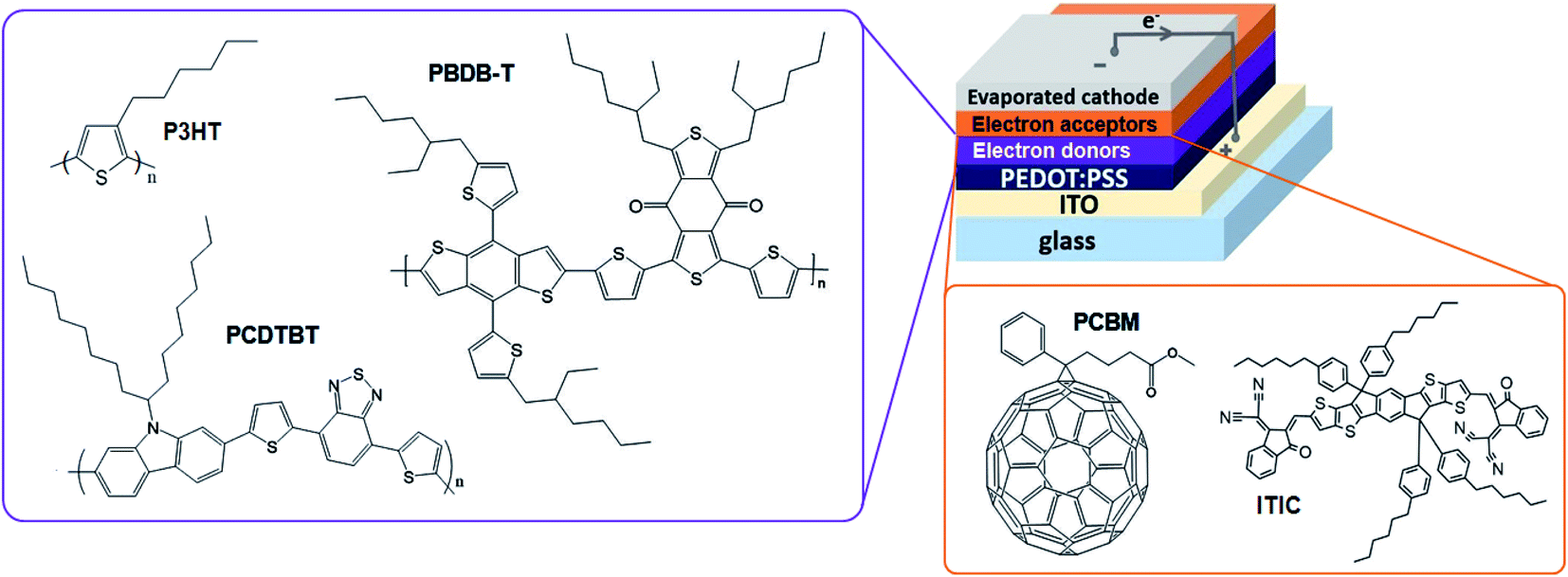
We elucidate the formation mechanism of adequate vertical concentration gradients in sequentially deposited poly(3-hexylthiophene-2,5-diyl) (P3HT) and phenyl-C61-butyric acid methyl ester (PCBM) bilayer solar cells. Using advanced analytical techniques, we clarify the origins of the enhanced photovoltaic performances of as-deposited and annealed bilayer P3HT/PCBM organic solar cells upon P3HT layer rubbing prior to PCBM deposition. Energy-dispersive X-ray spectroscopy reveals the individual effects of rubbing and annealing on the formation of adequate concentration gradients in the photoactive layers. Repetitive rubbing of P3HT strongly affects the active layer nanomorphology, forming an intermixed layer in the as-deposited devices which is retained after the annealing process. Infrared p-polarized multiple-angle incidence resolution spectrometry measurements indicate that rubbing induces a minor reorganization of the P3HT molecules in the polymer-only thin films towards face-on orientation. However, the deposition of the upper PCBM layer reverts the P3HT molecules back to their original orientation. These findings suggest that the formation of an adequate concentration gradient upon rubbing corresponds to the dominant contribution to the improved photovoltaic characteristics of rubbed bilayer organic solar cells. Using the reference low bandgap copolymer PCDTBT, we demonstrate that rubbing can be successfully applied to increase the photovoltaic performances of PCDTBT/PCBM organic solar cells. We also demonstrate that rubbing can be an efficient and versatile strategy to improve the power conversion efficiency of non-fullerene solar cells by using the reference materials in the field, PBDB-T and ITIC.
Introduction
Organic solar cells (OSCs) have drawn tremendous attention as they present several advantages such as being semi-transparent, flexible, low cost, lightweight and processable on a large-scale at low temperatures.1–6 Poly(3-hexylthiophene-2,5-diyl) (P3HT) and phenyl-C61-butyric acid methyl ester (PCBM) are considered as reference conjugated polymer electron donor and fullerene derivative electron acceptor employed in OSC active layers.7,8 Although most active layers are fabricated using co-deposition of the donor and acceptor materials into bulk heterojunctions (BHJs) thin films, sequential deposition of diffusive P3HT/PCBM bilayers (BLs) provides the possibility to independently tune the properties of each layer.9,10 BLs also offer the opportunity to form adequate donor/acceptor vertical concentration gradients in active layers for regular architecture OSCs, which can facilitate charge percolation to the electrodes and reduce leak currents.11 Unlike BHJ active layers that rely on highly unstable donor/acceptor intermixed networks, the phase separated active layer morphologies of BLs generally leads to longer device lifetimes.12,13 Furthermore, controlling the BHJ active layer nanomorphology during large-area coating may be difficult and thus the BL strategy is much more attractive for commercial production of OSCs. However, several studies argue that upon thermal annealing, similar concentration gradients and nanomorphologies are produced in both BHJ and BL active layers.14–16 On the other hand, alternative processes that do not rely on the use of orthogonal solvents such as lamination or transfer printing have also been employed to fabricate well-defined BL OSCs.17–19 However, when employing these processes, generating the intermixed layer to achieve high photocurrents in OSCs generally becomes more challenging and often requires a nanostructuration step.17 In other words, diffusive BLs prepared via sequential solvent deposition demonstrate a great potential for highly efficient and stable OSC fabrication as long as adequate donor–acceptor vertical concentration profiles are formed. We previously demonstrated that rubbing P3HT prior to PCBM deposition can enhance the performances of annealed (AND) BL OSCs through the formation of such adequate donor–acceptor vertical concentration profiles.20 Additionally, the application of pressure on the P3HT layer by uniaxial rubbing has been reported to be an effective strategy to change the molecular orientation of P3HT molecules from an edge-on to a face-on configuration.20,21Molecular reorientation from edge-on to face-on crystallites promotes intermolecular charge hopping in the vertical direction. Therefore, promoting edge-on to face-on molecular reorientation could contribute to improving the charge collection efficiency in the vertical OSC device architectures. This molecular reorientation to face-on is favorable for efficient charge transport in the direction normal to the electrodes of the BL device architecture.20,22 As our past investigation was limited to AND BL devices, we could not confirm whether the enhanced thin film properties should be attributed to rubbing, annealing or a combination of both processes.
Furthermore, assessing whether the adequate concentration profiles are formed prior to annealing is a key factor to potentially extend the use of rubbing to other donor/acceptor systems. If rubbing induces adequate donor/acceptor segregation in the BL OSC active layers, the application of rubbing could be extended to donor/acceptor systems based on low bandgap copolymers or non-fullerene acceptors (NFAs) that do not require annealing at high temperatures above 100 °C. The study of the individual impacts of rubbing and annealing on the performances of BL OSCs could thus open the path to highly efficient and air-stable OSC fabrication.13
In this study, we investigate the individual impacts of rubbing and thermal annealing on the vertical organization of the active materials in regular architecture BL P3HT/PCBM OSCs and on the orientation of P3HT molecules when a high regioregular P3HT (>98%) is used. Energy-dispersive X-ray spectroscopy (EDS) and p-polarized multiple-angle incidence resolution spectrometry (pMAIRS) are employed to measure the concentration gradient and molecular orientation in the thin films, respectively. Through these measurements, we clearly distinguish the effect of rubbing and annealing on the active layer nanomorphology, which we correlate with the photovoltaic (PV) characteristics of the devices. Our results suggest that rubbing forms adequate vertical concentration profiles which can be clearly observed in the active layers of as-deposited (ADP) and AND devices. In unrubbed OSCs, annealing induces aggregation of the active molecules in the P3HT/PCBM BL resulting in a segregation of PCBM molecules at both the top (Al electrode side) and buried (substrate side) interfaces of the active layer. Despite this inadequate vertical concentration profile, a large increase in PV performances can be observed in unrubbed ANDs with respect to unrubbed ADPs. The combination of rubbing and annealing forms ideal intermixed layers located between P3HT-rich and PCBM-rich crystalline layers at the buried and top interfaces, respectively. Although rubbing P3HT thin films leads to small reorganization of the P3HT molecules towards the face-on orientation, the subsequent PCBM deposition reverts them their original configuration. These findings suggest that the vertical concentration gradient resulting from rubbing and annealing contribute dominantly to the enhanced PV performances of the BL P3HT/PCBM OSCs. We also investigated other sequentially deposited BLs using low bandgap copolymers such as PCDTBT or PBDB-T combined with either PCBM or the NFA ITIC (see molecular structures in Fig. 1). Independently of the used donor/acceptor materials, the power conversion efficiencies (PCEs) of rubbed OSCs are higher than those of unrubbed ones. This confirms that rubbing is a simple yet efficient strategy to enhance the performances of BL OSCs independently of the crystalline nature of the electron donor and of the chemical nature of the electron acceptor.
 | ||
| Fig. 1 Chemical structures of the active materials and schematic representation of the BL OSC architectures. | ||
Experimental
Glass substrates coated with indium-tin-oxide (ITO) are ultrasonically cleaned in acetone, detergent, pure water and isopropyl alcohol, followed by a UV-ozone surface treatment for 30 min. The hole transport layer is formed by spin-coating an aqueous dispersion of poly(3,4-ethylenedioxythiophene)–poly(styrene sulfonate) (PEDOT:PSS) (Heraeus, Clevios P VP AI 4083) on the cleaned substrates at 4000 rpm for 30 s. P3HT (BASF Sepiolid P200, >98% regioregularity) is dissolved in chlorobenzene at a concentration of 30 mg mL−1. This solution is stirred for ca. 3 h at 50 °C and then spin-coated at 2500 rpm for 30 s to produce ca. 47 nm-thick P3HT layers. P3HT films are immediately rubbed as-cast without further drying. They are uniaxially rubbed 5, 10, 15 or 20 times by hand with a composite wiping cloth (Savina MX, KB Seiren, Ltd.) composed of polyester and nylon. The knit polyester/nylon composite yarn is split open resulting in a high filament density of 82![[thin space (1/6-em)]](https://www.rsc.org/images/entities/char_2009.gif) 550 filaments per cm2 on the cloth surface. The wiping cloth is folded and clipped at ca. 0.8 cm height (from the edge of clip to the point of contact between the wiping cloth and the samples) to minimize the variation of rubbing force. PCBM (Luminescence Technology) is dissolved in dichloromethane (DCM) to obtain a 10 mg mL−1 solution. This acceptor solution is spin-coated on top of the P3HT layers at 4000 rpm for 10 s to yield ca. 24 nm-thick PCBM layers. The preparation of P3HT/PCBM active layers is performed in a nitrogen-filled glove box with an oxygen concentration lower than 1%. Al electrodes (100 nm) are evaporated in high vacuum conditions with an evaporation rate of ca. 7 Å s−1. The encapsulation process is carried out in a glove box with an oxygen concentration of less than 1 ppm to prevent oxidation of the active layers and electrodes.
550 filaments per cm2 on the cloth surface. The wiping cloth is folded and clipped at ca. 0.8 cm height (from the edge of clip to the point of contact between the wiping cloth and the samples) to minimize the variation of rubbing force. PCBM (Luminescence Technology) is dissolved in dichloromethane (DCM) to obtain a 10 mg mL−1 solution. This acceptor solution is spin-coated on top of the P3HT layers at 4000 rpm for 10 s to yield ca. 24 nm-thick PCBM layers. The preparation of P3HT/PCBM active layers is performed in a nitrogen-filled glove box with an oxygen concentration lower than 1%. Al electrodes (100 nm) are evaporated in high vacuum conditions with an evaporation rate of ca. 7 Å s−1. The encapsulation process is carried out in a glove box with an oxygen concentration of less than 1 ppm to prevent oxidation of the active layers and electrodes.
Compared to P3HT, low bandgap copolymers such as PCDTBT and PBDB-T exhibit much higher stability in air, thus removing the necessity to perform rubbing in a nitrogen-filled glovebox.23,24 Enabling rubbing in air also considerably facilitates the fabrication process. The PCDTBT/PCBM bilayers are thus prepared in air by sequentially spin-coating PCDTBT (Sigma-Aldrich, Mw: 100000–140000) from a 3 mg mL−1 solution in o-dichlorobenzene (DCB) at 500 rpm for 90 s and PCBM from a 10 mg mL−1 DCM solution at 4000 rpm for 10 s. The resulting BLs have thicknesses between 60 and 75 nm. They are annealed at 70 °C for 10 min to remove any residual solvent trace prior to thermal evaporation of bathocuproine (10 nm) and Ag (65 nm) as cathode. The PBDB-T (Luminescence Technology, Mw > 10000) solution is prepared with a concentration of 10 mg mL−1 in DCB and spin-coated in air at 4000 rpm for 40 s. ITIC (Luminescence Technology) is dissolved in DCM to obtain a 10 mg mL−1 solution which is spin-coated on top of PBDB-T at 4000 rpm for 10 s. The resulting PBDB-T/ITIC BLs have thicknesses of approximately 120 nm and are annealed at 100 °C for 10 min prior to thermal evaporation of bathocuproine (10 nm) and Ag (65 nm) electrodes. Note that no solvent additive was employed for the PBDB-T/ITIC BL fabrication. The configuration of the OSC architecture is summarized in Fig. 1.
The PV performances of the devices are measured using a Keithley 2400 sourcemeter under 1 sun (AM1.5G, 100 mW cm−2) irradiation from a solar simulator. The data presented for P3HT/PCBM ADP BL OSCs corresponds to the average PV performances of 10 unrubbed devices or 10 rubbed devices each having an active area of 4 mm2. After measuring the P3HT/PCBM ADP device performances, they are annealed at 140 °C for 10 min to produce AND OSCs, which are characterized following the same procedure. The data on PCDTBT/PCBM BL OSCs corresponds to the PV performances without post-annealing for 4 unrubbed and 4 rubbed devices. Similarly, 4 unrubbed and 4 rubbed PBDB-T/ITIC BL OSCs were prepared. However, one of the unrubbed PBDB-T/ITIC BL OSC did not function properly and was thus removed from the average PV performance calculations. The results presented here thus correspond to the average of 3 unrubbed and 4 rubbed PBDB-T/ITIC BL OSCS, respectively. An optimized rubbing time of 10 was found for these OSCs in which all rubbed OSCs demonstrated considerably large improvements in PV performances with respect to unrubbed ones. The thickness and surface roughness of the active layers are measured using a Keyence VN-8000 Atomic Force Microscope (AFM).
The thicknesses of the individual layers are also measured by separately depositing the PEDOT:PSS, P3HT, PCDTBT, PBDB-T, PCBM and ITIC solutions on quartz substrates. The element mapping of the ADP and AND P3HT/PCBM devices' cross-sections is performed using a JEOL JEM-ARM200F scanning transmission electron microscope with integrated EDS measurement. The molecular orientation of the P3HT and P3HT/PCBM films are evaluated with a Thermo Fisher Scientific Nicolet 6700 Fourier-transform infrared spectrometer equipped with an automatic pMAIRS equipment. Each sample is measured twice to remove potential inconsistencies.
Results and discussion
The effect of rubbing on short-circuit current density (Jsc), open-circuit voltage (Voc) and fill factor (FF) of the ADP and AND BL devices is shown in the current density–voltage (J–V) curves presented in Fig. 2. A quantitative comparison of the PV characteristics from all the OSCs, including their power conversion efficiency (PCE), can be found in Table 1 and Fig. S1.† Significant increases of Jsc, Voc and FF are observed in the 5 times-rubbed ADP devices with respect to the unrubbed ADPs, producing a large enhancement of the average PCE.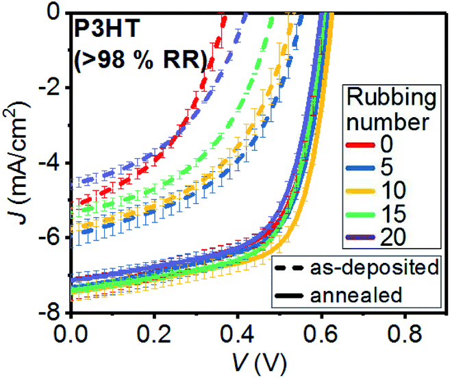 | ||
| Fig. 2 Average J–V curves under illumination from 10 ADP and AND P3HT/PCBM OSCs with different rubbing times. | ||
| Rubbing number | Voc (V) | Jsc (mA cm−2) | FF | PCE (%) | ||||
|---|---|---|---|---|---|---|---|---|
| ADP | AND | ADP | AND | ADP | AND | ADP | AND | |
| 0 | 0.37 ± 0.01 | 0.61 ± 0.00 | 5.19 ± 0.14 | 7.37 ± 0.30 | 0.43 ± 0.01 | 0.62 ± 0.01 | 0.83 ± 0.03 | 2.78 ± 0.09 |
| 5 | 0.56 ± 0.01 | 0.62 ± 0.00 | 5.94 ± 0.32 | 7.33 ± 0.36 | 0.48 ± 0.00 | 0.63 ± 0.02 | 1.58 ± 0.11 | 2.86 ± 0.09 |
| 10 | 0.54 ± 0.01 | 0.63 ± 0.00 | 5.75 ± 0.08 | 7.45 ± 0.25 | 0.48 ± 0.01 | 0.66 ± 0.00 | 1.47 ± 0.07 | 3.09 ± 0.11 |
| 15 | 0.48 ± 0.01 | 0.60 ± 0.01 | 5.33 ± 0.14 | 7.40 ± 0.10 | 0.46 ± 0.01 | 0.63 ± 0.01 | 1.21 ± 0.03 | 2.89 ± 0.02 |
| 20 | 0.41 ± 0.02 | 0.60 ± 0.00 | 4.48 ± 0.12 | 7.14 ± 0.08 | 0.43 ± 0.00 | 0.63 ± 0.01 | 0.83 ± 0.01 | 2.70 ± 0.07 |
However, a decrease in the PV characteristics of the devices is observed when the rubbing number is increased up to 20 times. After the annealing step, the BL OSCs clearly exhibit improved charge carrier extraction as demonstrated by the enhanced Voc and FF values. As a result, the rubbed AND devices exhibit less striking increments of their PV characteristics with respect to the rubbed ADP BL OSCs. Particularly, there is almost no change in Jsc and Voc with increasing rubbing number up to 20 times in AND devices. The FF of the OSCs gradually increases from 0.62 to 0.66 with rubbing up to 10 times and then decreases to 0.63 when P3HT layers are rubbed more than 10 times. Unlike the PCE evolution for AND devices, which follows the FF trend, the PV characteristics of ADP devices are mainly influenced by the differences in their Voc values.
Rubbing locally removes P3HT from the surface of the deposited films and thus a P3HT thickness reduction can be observed with increasing rubbing number (Table 2). Thin P3HT layers have low series resistances leading to efficient hole collection in P3HT/PCBM BL-OSCs. However, because PCBM molecules gradually diffuse inside the P3HT layer, decreasing the thickness of the P3HT layer generally leads to increased leak currents. Thickness reduction of the P3HT layers thus has opposite impacts on the FF of P3HT/PCBM BL OSCs. The unrubbed P3HT/PCBM BLs presented in this study have been optimized in terms of P3HT thickness to achieve the highest FF and PCE. Although we cannot fully exclude the fact that P3HT thickness reduction could contribute to the increased FF observed for rubbed BLs, the minor change in P3HT thickness (within 2.5 nm up to 10 rubbing times) should not significantly influence the PV performances of BL OSCs. The localized material removal also produces uniaxial grating-like topographies on the rubbed P3HT surfaces (Fig. S2†). The maximum heights of the ADP P3HT topographic profiles (Ry) indicate that rubbing up to 10 times gradually reduces the surface roughness of the conjugated polymer films from 22.5 to 13.5 nm. Additional rubbings of the ADP P3HT films up to 20 times result in a gradual increase of Ry from 13.5 back to 21.1 nm, a value comparable to the unrubbed films Ry (22.5 nm). The variations of the surface roughness and thickness of P3HT films may influence the degree of PCBM diffusion into the underlying ADP P3HT layer. In fact, the individual thicknesses of P3HT (47 nm) and PCBM layers (24 nm) would result in a combined value of 71 nm. The unrubbed P3HT/PCBM BLs have a thickness of 58.5 nm which already confirms that PCBM molecules penetrate into the P3HT layer. Increasing number of rubbing gradually reduce the thickness of P3HT layers from 46.8 nm to 43.2 nm. Compared to this small thickness reduction, the impact of rubbing on the BL is much more remarkable. Although the thickness of 10 times-rubbed P3HT films is only reduced by 2.5 nm with respect to the unrubbed layers, the resulting BLs exhibit a large thickness difference of approximately 10 nm. Interestingly, the 20 times-rubbed P3HT films and BLs have a similar thickness around 43 nm suggesting that PCBM molecules diffuse entirely within the underlying polymer layer.
| Rubbing number | Thickness (nm) | Ry (nm) | |
|---|---|---|---|
| P3HT | P3HT/PCBM | P3HT | |
| 0 | 46.8 ± 0.6 | 58.5 ± 0.8 | 22.5 ± 6.9 |
| 5 | 45.4 ± 0.3 | 52.3 ± 1.8 | 19.8 ± 6.8 |
| 10 | 44.3 ± 0.4 | 49.1 ± 0.2 | 13.5 ± 1.2 |
| 15 | 43.5 ± 0.1 | 46.2 ± 0.1 | 15.7 ± 1.5 |
| 20 | 43.2 ± 0.7 | 43.0 ± 0.5 | 21.1 ± 3.5 |
Nevertheless, clear and quantitative data regarding the diffusion depth of PCBM into P3HT layers cannot be obtained from the thickness measurements alone. We perform EDS elemental mapping of the device cross-sections to estimate the amount of PCBM diffusing into the P3HT layers for each deposition condition (Fig. 3). The detected elements [blue: indium (In), green: sulfur (S), black: carbon (C) and red: (Al)] correlate well with the device configuration, namely, glass/ITO/PEDOT:PSS (39 nm)/P3HT/PCBM BLs (40–60 nm)/Al (100 nm). Since P3HT contains sulfur, the sulfur profiles (white line in Fig. 3) within the 50–90 nm region reflect the location of P3HT in the active layer. For the region of 80–120 nm, sulfur from the PEDOT:PSS layer is detected. The sulfur profile of the unrubbed ADP device in Fig. 3(a) reveals that a significant amount of P3HT can be found at the top interface of the active layers next to the Al electrode.
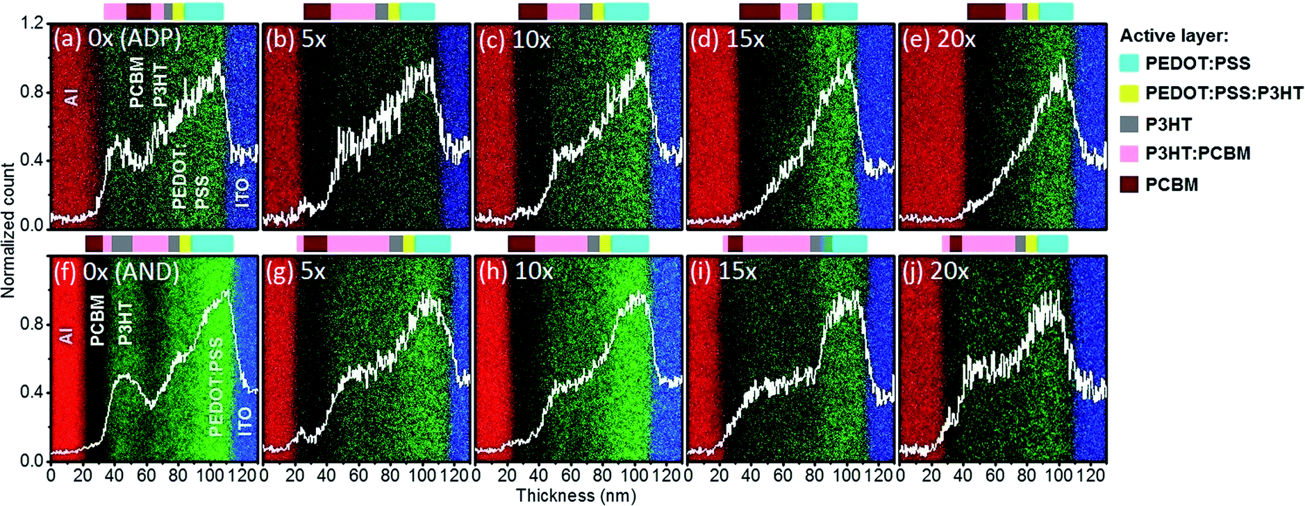 | ||
| Fig. 3 The cross-sectional EDS element mappings of ADP P3HT/PCBM devices corresponding to (a) 0, (b) 5, (c) 10, (d) 15 and (e) 20 times rubbing; and AND P3HT/PCBM devices corresponding to (f) 0, (g) 5, (h) 10, (i) 15 and (j) 20 times rubbing. The detected elements are indium (blue), sulfur (green), carbon (black) and aluminum (red). The white line represents the normalized sulfur profile. The color scales above the EDS images indicate the estimated active layer composition based on the normalized sulfur profiles. | ||
In regular device architectures, an electron donor-rich layer at the top interface increases the probability for charge recombination which is consistent with the low Voc values measured for the unrubbed ADP devices (Table 1).25,26 When the P3HT layer is rubbed prior to PCBM deposition, such P3HT-rich layer is not found near the Al electrode (Fig. 3(b)–(e)). This change effectively reduces charge recombination in rubbed ADP devices. In the 5 times-rubbed ADP OSCs, the decrease of P3HT concentration near Al significantly increases its Voc from 0.37 to 0.56 V.
The sulfur profile in Fig. 3(b) indicates that a layer with equally mixed P3HT and PCBM (intermixed layer) is formed between 40 nm and 70 nm which is covered with a PCBM-rich layer located between 20 nm and 40 nm. Such concentration profile enables efficient charge generation and transport to the respective electrodes. Consequently, the Jsc and FF of the 5 times-rubbed ADPs increase from 5.19 to 5.94 mA cm−2 and 0.43 to 0.48, respectively, compared to the reference unrubbed BL OSCs. Increasing the rubbing repetitions up to 15 times (Fig. 3(d)) induces a deeper diffusion of PCBM towards the PEDOT:PSS region, which in turn promotes losses due to charge recombination or leak currents and substantially reduces the Voc from 0.54 V (10 times-rubbed devices) to 0.48 V (15 times-rubbed devices).27 The narrowing of the intermixed layer in the 15 times-rubbed device results in lower charge generation leading to reduced Jsc and FF of 5.33 mA cm−2 and 0.46 for 15 times-rubbed OSCs with respect to the Jsc and FF values of 5.75 mA cm−2 and 0.48 for 10 times-rubbed OSCs. Despite nearly identical sulfur profiles for 15 times and 20 times-rubbed devices, the thinner 20 times-rubbed active layers further decrease the Voc, Jsc and FF to 0.41 V, 4.48 mA cm−2 and 0.43 respectively. This confirms our hypothesis that excessive P3HT removal during rubbing (e.g., in 20 times-rubbed active layers) produces active layers in which PCBM overly diffuses into the P3HT layer, which results in a reduction of the underlying P3HT thickness. In summary, the compositional studies of the ADP devices suggest that adequate vertical profiles are produced when P3HT films are rubbed 5 or 10 times. It is essential to assess whether these profiles are maintained upon annealing of the devices.
In both P3HT/PCBM BHJs and BLs, thermal annealing induces aggregation of the electron donor and electron acceptor molecules which modifies the vertical concentration profiles in the active layers.16,28,29 Our results on ADP and AND P3HT/PCBM BLs clearly indicate that upon thermal annealing PCBM molecules aggregate at the top interface of the active layers next to the Al electrode (Fig. 3(f)–(j)). This result is consistent with previous observations of the impact of thermal annealing on the active layer nanomorphology.28,29 The phase-segregated nanomorphology produced in AND active layers can considerably reduce recombination losses and simultaneously enhance charge transport.27,30 In fact, these two positive effects of annealing can be clearly observed by comparing the PV characteristics of unrubbed ADP and AND devices. Upon annealing, the reduction of recombination losses lead to a Voc increased from 0.37 V in the ADP devices to 0.61 V in the AND devices. A more efficient charge transport resulting from adequate concentration gradients and partial crystallization of the materials through aggregation also enhances the Jsc and FF from 5.19 to 7.37 mA cm−2 and from 0.43 to 0.62, respectively. Nevertheless, as the ADP unrubbed active layers initially have P3HT-rich layer in contact with the top Al electrode, upon thermal annealing and diffusion of the PCBM molecules at the top interface, the P3HT-rich layer is confined towards the center of the AND active layers (Fig. 3(f)).
These profiles suggest that even higher PV performances could be expected from AND active layers with ideal vertical concentration gradients. EDS elemental mappings of ADP active layers clearly indicate that rubbing provides a simple solution to avoid the formation of a P3HT-rich layer at the top interface prior to thermal annealing (Fig. 3(a)–(e)). Fig. 3(g)–(j) evidence that, similarly to unrubbed ANDs, P3HT-free top interfaces are produced in ANDs fabricated from BLs rubbed 5 or 10 times.
Our results demonstrate that the thickness of P3HT-free top layer is gradually reduced with increasing number of rubbing above 10 times, which is consistent with the active layer thickness variation presented above. Additionally, large intermixed layers with evenly distributed P3HT:PCBM ratios are formed in the rubbed ANDs within the 40–90 nm region independently of the rubbing number (Fig. 3(g)–(j)). Such layers composed of intimately mixed electron donor and electron acceptor materials further enhance the charge generation efficiency within the active layer.27,31 These observations correlate well with the PV performances of AND devices (Table 1). The absence of P3HT near the Al electrodes combined with the large intermixed layer produce the highest Voc (0.63 V), Jsc (7.45 mA cm−2) and FF (0.66) in the 10 times-rubbed OSCs. As the top PCBM buffer layer gradually disappears in 15 and 20 times-rubbed ANDs, the increased amount of P3HT near the Al electrodes results in more charge recombination compared to the 10 times-rubbed devices. From these compositional studies, we can clearly conclude that annealing leads to large improvements in PV performances of the BL OSCs through the formation of a P3HT-free top interface which promotes efficient electron collection at the Al electrode and induces crystallization of the materials. However, the active layer composition in the bulk and at the buried interface is not strongly affected by thermal annealing. On the other hand, rubbing already produces adequate concentration gradients in the ADP active layers with most P3HT molecules found in the bulk or at the buried interface of the rubbed ADPs. For 5 and 10 times-rubbed BLs, no major change can be observed in the vertical concentration profiles upon thermal annealing, whereas for larger rubbing times, annealing promotes the formation of intermixed layers. As the P3HT-free top interface is formed in unrubbed ANDs, our EDS results provide clear evidence to explain the lower impact that rubbing has on the PV performances of AND OSCs as compared to those of ADP devices (Fig. S1†).
To investigate the influence of rubbing on the molecular orientation at the surface of P3HT layer, pMAIRS measurements are performed on P3HT films with increasing rubbing times. Molecular aggregation in very thin polymorph films is generally analyzed by the grazing incident X-ray diffraction (GIXRD) technique but combining GIXRD and pMAIRS enables a more accurate morphological characterization of the thin films.32,33 In fact, molecular orientation of polymeric thin films is often overlooked by XRD-based techniques because of their poor crystallinity.33,34 Unidirectional hole transport in highly ordered P3HT thin films can be enhanced through crystallite reorientation.22 However, in semi-crystalline P3HT films, the amorphous domains linking adjacent crystallites correspond to the limiting factor when it comes to hole transport.35
Therefore, the fact that orientation of P3HT chains could facilitate charge hopping even in the relatively disordered amorphous phase cannot be overlooked as it may have a large impact on the hole transport properties in P3HT thin films. In this sense, pMAIRS may be the adequate technique to probe unrubbed and rubbed P3HT-based samples as it provides information on molecular orientation for each chemical group irrespective of the thin film crystallinity.32,36 In fact, pMAIRS has been previously employed to reveal structural details that are often missed by GIXRD.37,38
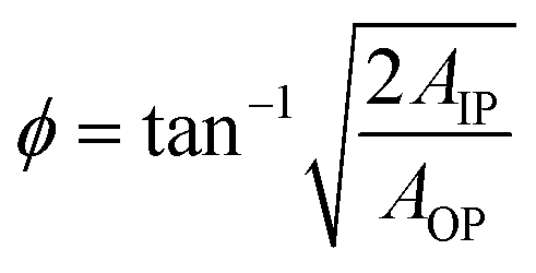
The in-plane (IP) and out-of-plane (OP) infrared (IR) absorbance spectra of P3HT and P3HT/PCBM films are shown in Fig. 4(a)–(d). The thiophene ring vibration [ν(C![[double bond, length as m-dash]](https://www.rsc.org/images/entities/char_e001.gif) C)] mode is observed at ca. 1510 cm−1 while the C–H out-of-plane deformation vibration [γ(C–H)] mode on the thiophene ring appears at ca. 820 cm−1.39 The transition moment of a vibrational mode serves as an indicator to discuss the molecular orientation in a thin film.39 The polymer backbone is parallel to the transition moment of the ν(CC) mode while the thiophene ring is perpendicular to that of the γ(C–H) mode.39,40 By taking into account the band intensities of the OP spectrum (AOP) and the IP spectrum (AIP), the orientation angle (ϕ) can be calculated using the following equation.39
C)] mode is observed at ca. 1510 cm−1 while the C–H out-of-plane deformation vibration [γ(C–H)] mode on the thiophene ring appears at ca. 820 cm−1.39 The transition moment of a vibrational mode serves as an indicator to discuss the molecular orientation in a thin film.39 The polymer backbone is parallel to the transition moment of the ν(CC) mode while the thiophene ring is perpendicular to that of the γ(C–H) mode.39,40 By taking into account the band intensities of the OP spectrum (AOP) and the IP spectrum (AIP), the orientation angle (ϕ) can be calculated using the following equation.39
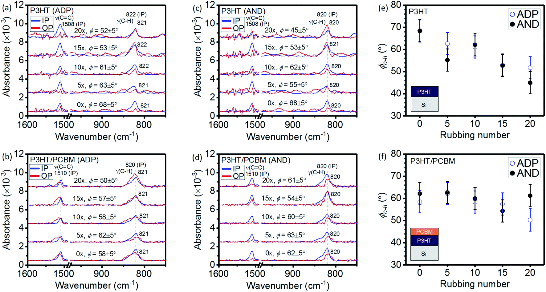 | ||
| Fig. 4 The IR pMAIRS absorbance spectra of ADP (a) P3HT and (b) P3HT/PCBM films along with AND (c) P3HT and (d) P3HT/PCBM films with different rubbing times on P3HT films; the orientation angles of (e) P3HT and (f) P3HT/PCBM films calculated from IR pMAIRS absorbance spectra in ADP and AND conditions with different rubbing times on P3HT films. (e) and (f) Exhibit typical error bars obtained for the pMAIRS measurements, namely, ±5°. | ||
The pMAIRS spectra of the unrubbed ADP P3HT films show the presence of strong ν(CC) and γ(C–H) bands in the IP spectrum, indicating an edge-on molecular orientation with a calculated orientation angle of the γ(C–H) mode from the surface normal of ϕC–H = 68°. Interestingly, in the spectrum of 5 times-rubbed P3HT films, the OP peak appears at 821 cm−1 [γ(C–H)] and rubbing is found to align the P3HT molecules to ϕC–H = 63°. The γ(C–H) OP band increases with rubbing times, reducing ϕC–H to 52° in 20 times-rubbed film (Fig. 4(a)). pMAIRS typically generates measurement deviations of ±5°.38 As a result, molecular reorientations should be considered notable when the changes in ϕC–H largely exceed 10°. Nevertheless, the trends and values obtained for ADP P3HT films imply that the P3HT molecules are gradually aligned towards the face-on orientation with increasing rubbing number. Meanwhile, the intensities of ν(CC) and γ(C–H) modes in IP and OP spectra of AND P3HT films follow the same trends as ADP films (Fig. 4(c) and (e)). These results indicate that annealing does not significantly change the orientation of P3HT molecules in P3HT single layer.
Deposition of the PCBM coating layer can significantly affect molecular orientation in the underlying P3HT films. Therefore, to understand if the enhanced performances observed in rubbed P3HT/PCBM BL OSCs can be correlated with molecular reorientation, we perform the structural studies on ADP and AND BLs. Unrubbed ADP and AND P3HT/PCBM BLs exhibit ϕC–H values of 58° and 62°, respectively (Fig. 4(b) and (d)). As the difference between the ϕC–H values for P3HT single layers and P3HT/PCBM BLs are within the experimental error, we can conclude that deposition of the PCBM layer does not significantly change the molecular orientation in unrubbed P3HT thin films (Fig. 4(e) and (f)). Independently of the rubbing number, ADP BLs exhibit ϕC–H values between 57° and 62° up to 15 rubs (Fig. 4(b) and (f)). This clearly indicates that the large FF enhancements in ADP BL devices rubbed up to 15 times cannot be ascribed to molecular reorientation in the P3HT layer (Table 1). Similarly, after undergoing the annealing treatment, the band intensities of the OP peaks remain almost unchanged regardless of the rubbing number (Fig. 4(d)). Hence, the ϕC–H are seemingly steady across the AND BLs with measured values between 54° and 61° (Fig. 4(d)). Once again, such small variations cannot be correlated with the notable FF enhancements observed in rubbed AND BLs with respect to unrubbed ones (Table 1). All the above observations strongly suggest that the slight change of molecular orientation upon rubbing plays a less essential role than the formation of adequate concentration gradients for determining the device performance.
Note that some error may also originate from the reproducibility of the rubbing process when rubbing is performed by hand. In fact, automatization of the rubbing process is an essential step to ensure that the rubbing strategy provides reliable improvements in BL OSC performances independently of the operator fabricating the devices. Through our initial experiments (see set-up in Fig. S3†), we have verified that similar enhancements of the PV performances of BL OSCs can be achieved with hand rubbing and automated rubbing (Table S1†). The small differences observed between hand and machine rubbed performance increases could be due to variations in applied pressure. Optimization of applied pressure could thus result in higher performances for machine rubbed devices but this is outside the scope of this study. Furthermore, before suggesting rubbing as a universal strategy to improve the performances of BL OSCs, the versatility of the process with respect to the employed materials should be elucidated. Unlike the highly crystalline P3HT, PCDTBT is an amorphous material that generally yields higher PV performances at processing temperatures below 100 °C.41–43 However, previous attempts to produce ADP PCDTBT-based BL OSCs resulted in fairly poor PV performances.44 In fact, Seok et al. proposed to use solvent additives to promote the formation of adequate vertical concentration gradients in PCDTBT/PCBM BLs. When solvent additives are included in the PCDTBT layer, the PCE of their BL OSCs increase from 1.09% (no additives) to 1.82% (with additives). On the other hand, when a solvent additive was used for PCBM deposition, the PCE increased to 2.88%. Finally, when both the donor and acceptor layers were deposited with solvent additives, a PCE value of 7.12% was achieved.
Unlike the BL devices by Seok et al. that employ C70-PCBM, we used C60-PCBM to maintain similar preparation conditions as for the P3HT/PCBM devices discussed above. C70-PCBM generally yields a higher Jsc in PCDTBT-based OSCs as compared to C60-PCBM. Our reference unrubbed devices exhibit a relatively high Voc of 0.83 V which, associated with a Jsc of 9.84 mA cm−2 and a FF of 0.42, produces an average PCE of 3.46% (Table 3 and Fig. 5). Note that, as DCB was used as solvent for the PCDTBT layer, the deposited PCDTBT films were given sufficient time (typically 1 h) to entirely dry prior to rubbing and/or PCBM deposition. Similarly to P3HT/PCBM ADP OSCs, a notable improvement in device performances can be observed upon rubbing the PCDTBT layer prior to PCBM deposition. The Jsc, Voc, FF and PCE reach values of 10.05 mA cm−2, 0.88 V, 0.45 and 3.97%, respectively, thus producing a PCE 15% higher than unrubbed BLs. Note that post-annealing of the PCDTBT/PCBM BLs at 70 °C does not remarkably affect the device performances. Our results thus point out that, unlike the hard to control solvent addition techniques, rubbing can be a good alternative for the fabrication of efficient PCDTBT-based BLs without using any solvent additives.
| BL OSCs | Rubbing number | Voc (V) | Jsc (mA cm−2) | FF | PCE (%) |
|---|---|---|---|---|---|
| PCDTBT/PCBM | 0 | 0.83 ± 0.01 | 9.74 ± 0.33 | 0.42 ± 0.01 | 3.41 ± 0.18 |
| 10 | 0.87 ± 0.01 | 10.09 ± 0.11 | 0.45 ± 0.00 | 3.96 ± 0.04 | |
| PBDB-T/ITIC | 0 | 0.76 ± 0.03 | 7.45 ± 0.37 | 0.57 ± 0.00 | 3.21 ± 0.12 |
| 10 | 0.87 ± 0.00 | 8.59 ± 0.01 | 0.60 ± 0.01 | 4.48 ± 0.09 |
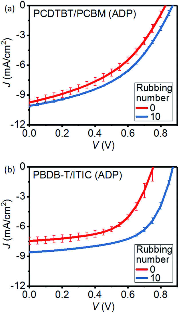 | ||
| Fig. 5 Average J–V curves under illumination from 4 devices of unrubbed and 10 times-rubbed (a) PCDTBT/PCBM and (b) PBDB-T/ITIC BL OSCs. | ||
Combining highly crystalline low bandgap copolymers such as PBDB-T with NFAs such as ITIC has recently opened the path to fullerene-free OSCs with PCEs regularly overcoming 10%. In fact, previous studies have demonstrated that PBDB-T can be combined with a well-designed NFA into BLs that produce similar morphologies as BHJs thus achieving PCEs up to 10.04%.45 Note that, PBDB-T/ITIC BLs fabricated in the same study yield a lower average PCE of 5.8%. Furthermore, BL OSCs employing recently developed donors and non-fullerene acceptors that produce high PCEs above 16% have also been recently reported.46 Nevertheless, we focus on PBDB-T/ITIC as these materials correspond to the most studied donor/acceptor pair for non-fullerene OSCs. Rubbed devices exhibit large enhancements in Voc with respect to unrubbed OSCs, which is consistent with the results obtained for fullerene-based ADPs. In addition to the Voc increase, Jsc is enhanced by approximately 15%, a behavior similar, once again, to that of P3HT/PCBM ADPs. As a result, despite being deposited in air without using solvent additives, the average PCE of rubbed PBDB-T/ITIC BL OSCs exhibits a relatively high value of 4.5% compared to unrubbed OSCs with a PCE of 3.2%.
Conclusions
By controlling the diffusion of PCBM molecules into the underlying P3HT layer in diffusive BL OSCs, we are able to fabricate ADP devices which exhibit a significant increase in PCE from 0.83% (unrubbed) to 1.58% (5 times-rubbed). In unrubbed devices, annealing results in the formation of a phase segregated PCBM layer at the top interface of the photoactive layer, which brings about a substantial increase of PCE from 0.83% (ADP) to 2.78% (AND). The combination of rubbing and thermal annealing further increases the PCE of P3HT/PCBM BLs in regular architecture OSCs to 3.09% (10 times-rubbed). Our results clearly demonstrate that rubbing the P3HT layer prior to PCBM deposition has a major impact on the nanomorphology of the resulting active layers. In particular, rubbing the ADP active layers yields adequate vertical concentration gradients. Annealing further improves the concentration profiles of the rubbed BLs through the formation of equally mixed interlayers capped with PCBM buffer layers. Despite the lack of edge-on to face-on molecular reorientation in P3HT/PCBM BLs, higher FF can be measured in the rubbed AND devices compared to the rubbed ADP OSCs, which confirms that adequate concentration profiles strongly impact the charge extraction properties of the devices. The interfacial and bulk properties obtained from the morphological and compositional studies consequently point out the importance of controlling the concentration gradient of the active layer to achieve high performances in both ADP and AND BL OSCs. As producing efficient OSCs at low processing temperatures is essential to fabricate sustainable devices, we further emphasize the applicability of rubbing to active layers materials processable at low temperatures by fabricating PCDTBT/PCBM BL OSCs. Compared to unrubbed PCDTBT/PCBM BLs which yield a PCE of around 3.4%, the corresponding rubbed OSCs demonstrate a remarkable increase in performances and produce a PCE of ca. 4%. Furthermore, our experiments also indicate that rubbing is not limited to fullerene-based OSCs but that it could also become a clever strategy to easily improve the PV performances of non-fullerene BL active layers. Our results also suggest that rubbing could be applied to any conjugated polymer materials independently of their crystallinity to form BL active layers with adequate vertical concentration profiles for regular architecture OSCs. Unlike thermal annealing which can be hard to control in highly crystalline systems (stronger phase separation) or have low impact in amorphous systems (e.g., PCDTBT), rubbing is a simple method that yields large PCE increases in ADP BL OSCs.Conflicts of interest
There are no conflicts to declare.Acknowledgements
The experimental work was supported by the Japan Society for the Promotion of Science through the Grant-in-aid for Young Scientists (B) program (Grant No. 17K14549) and by the NF Foundation through the R&D Encouragement Award.References
- R. Søndergaard, M. Hösel, D. Angmo, T. T. Larsen-Olsen and F. C. Krebs, Mater. Today, 2012, 15, 36–49 CrossRef.
- B. Yin, Q. Liu, L. Yang, X. Wu, Z. Liu, Y. Hua, S. Yin and Y. Chen, J. Nanosci. Nanotechnol., 2020, 10, 1934–1938 CrossRef.
- F. C. Krebs, Sol. Energy Mater. Sol. Cells, 2009, 93, 394–412 CrossRef CAS.
- O. Inganäs, Adv. Mater., 2018, 30, 1800388 CrossRef.
- P. R. Berger and M. Kim, J. Renewable Sustainable Energy, 2018, 10, 013508 CrossRef.
- T. Sano, S. Inaba and V. Vohra, ACS Appl. Energy Mater., 2019, 2, 2534–2540 CrossRef CAS.
- W. Ma, C. Yang, X. Gong, K. Lee and A. J. Heeger, Adv. Funct. Mater., 2005, 15, 1617–1622 CrossRef CAS.
- M. T. Dang, L. Hirsch and G. Wantz, Adv. Mater., 2011, 23, 3597–3602 CrossRef CAS.
- A. Loiudice, A. Rizzo, M. Biasiucci and G. Gigli, J. Phys. Chem. Lett., 2012, 3, 1908–1915 CrossRef CAS.
- V. Vohra, K. Higashimine, T. Murakami and H. Murata, Appl. Phys. Lett., 2012, 101, 173301 CrossRef.
- V. Vohra, K. Higashimine, S. Tsuzaki, K. Ohdaira and H. Murata, Thin Solid Films, 2014, 554, 41–45 CrossRef CAS.
- S. Dong, K. Zhang, B. Xie, J. Xiao, H. Yip, H. Yan, F. Huang and Y. Cao, Adv. Energy Mater., 2019, 9, 1802832 CrossRef.
- P. Cheng, C. Yan, Y. Wu, S. Dai, W. Ma and X. Zhan, J. Mater. Chem. C, 2016, 4, 8086–8093 RSC.
- S. A. Hawks, J. C. Aguirre, L. T. Schelhas, R. J. Thompson, R. C. Huber, A. S. Ferreira, G. Zhang, A. A. Herzing, S. H. Tolbert and B. J. Schwartz, J. Phys. Chem. C, 2014, 118, 17413–17425 CrossRef CAS.
- J. S. Moon, C. J. Takacs, Y. Sun and A. J. Heeger, Nano Lett., 2011, 11, 1036–1039 CrossRef CAS.
- K. H. Lee, P. E. Schwenn, A. R. G. Smith, H. Cavaye, P. E. Shaw, M. James, K. B. Krueger, I. R. Gentle, P. Meredith and P. L. Burn, Adv. Mater., 2011, 23, 766–770 CrossRef CAS.
- W. Wiedemann, L. Sims, A. Abdellah, A. Exner, R. Meier, K. P. Musselman, J. L. MacManus-Driscoll, P. Müller-Buschbaum, G. Scarpa, P. Lugli and L. Schmidt-Mende, Appl. Phys. Lett., 2010, 96, 263109 CrossRef.
- M. Campoy-quiles, T. Ferenczi, T. Agostinelli, P. G. Etchegoin, Y. Kim, T. D. Anthopoulos, P. N. Stavrinou, D. D. C. Bradley and J. Nelson, Nat. Mater., 2008, 7, 158–164 CrossRef CAS.
- V. Vohra, T. Anzai, S. Inaba, W. Porzio and L. Barba, Sci. Technol. Adv. Mater., 2016, 17, 530–540 CrossRef CAS.
- V. Vohra, G. Arrighetti, L. Barba, K. Higashimine, W. Porzio and H. Murata, J. Phys. Chem. Lett., 2012, 3, 1820–1823 CrossRef CAS.
- D. Kajiya, S. Ozawa, T. Koganezawa and K. I. Saitow, J. Phys. Chem. C, 2015, 119, 7987–7995 CrossRef CAS.
- L. Hartmann, K. Tremel, S. Uttiya, E. Crossland, S. Ludwigs, N. Kayunkid, C. Vergnat and M. Brinkmann, Adv. Funct. Mater., 2011, 21, 4047–4057 CrossRef CAS.
- X. Du, T. Heumueller, W. Gruber, A. Classen, T. Unruh, N. Li and C. J. Brabec, Joule, 2019, 3, 215–226 CrossRef CAS.
- T. Uchiyama, T. Sano, Y. Okada-shudo and V. Vohra, J. Mater. Chem. C, 2020, 8, 7162–7169 RSC.
- B. G. Kim, E. J. Jeong, H. J. Park, D. Bilby, L. J. Guo and J. Kim, ACS Appl. Mater. Interfaces, 2011, 3, 674–680 CrossRef CAS.
- S. B. Hacène and T. Benouaz, Phys. Status Solidi A, 2014, 211, 862–868 CrossRef.
- V. S. Gevaerts, L. J. A. Koster, M. M. Wienk and R. A. J. Janssen, ACS Appl. Mater. Interfaces, 2011, 3, 3252–3255 CrossRef CAS.
- V. Vohra, N. T. Razali and H. Murata, in Science and Applications of Tailored Nanostructures, ed. P. Di Sia, One Central Press, Manchester, 1st edn, 2017, ch. 7, pp. 128–147 Search PubMed.
- A. Orimo, K. Masuda, S. Honda, H. Benten, S. Ito, H. Ohkita and H. Tsuji, Appl. Phys. Lett., 2010, 96, 043305 CrossRef.
- K. A. Mazzio and C. K. Luscombe, Chem. Soc. Rev., 2014, 44, 78–90 RSC.
- H. Ohkita and S. Ito, Polymer, 2011, 52, 4397–4417 CrossRef CAS.
- N. Shioya, R. Murdey, K. Nakao, H. Yoshida, T. Koganezawa, K. Eda, T. Shimoaka and T. Hasegawa, Sci. Rep., 2019, 9, 579 CrossRef.
- T. Nakamura, N. Shioya, T. Shimoaka, R. Nishikubo, T. Hasegawa, A. Saeki, Y. Murata, R. Murdey and A. Wakamiya, Chem. Mater., 2019, 31, 1729–1737 CrossRef CAS.
- M. Hada, N. Shioya, T. Shimoaka, K. Eda, M. Hada and T. Hasegawa, Chem.–Eur. J., 2016, 22, 16539–16546 CrossRef CAS.
- S. Nam, S. Lee, I. Lee, M. Shin, H. Kim and Y. Kim, Nanoscale, 2011, 3, 4261–4269 RSC.
- T. Hasegawa and N. Shioya, Bull. Chem. Soc. Jpn., 2020, 93, 1127–1138 CrossRef CAS.
- T. Hasegawa, Anal. Chem., 2007, 79, 4385–4389 CrossRef CAS.
- T. Hasegawa, J. Phys. Chem. B, 2002, 106, 4112–4115 CrossRef CAS.
- N. Shioya, T. Shimoaka, K. Eda and T. Hasegawa, Macromolecules, 2017, 50, 5090–5097 CrossRef CAS.
- N. Shioya, T. Shimoaka and T. Hasegawa, Chem. Lett., 2014, 43, 1198–1200 CrossRef CAS.
- T. Wang, A. J. Pearson, A. D. F. Dunbar, P. A. Staniec, D. C. Watters, H. Yi, A. J. Ryan, R. A. L. Jones, A. Iraqi and D. G. Lidzey, Adv. Funct. Mater., 2012, 22, 1399–1408 CrossRef CAS.
- J. W. Kingsley, P. P. Marchisio, H. Yi, A. Iraqi, C. J. Kinane, S. Langridge, R. L. Thompson, A. J. Cadby, A. J. Pearson, D. G. Lidzey, R. A. L. Jones and A. J. Parnell, Sci. Rep., 2014, 4, 5286 CrossRef CAS.
- S. Inaba, R. Arai, G. Mihai, O. Lazar, C. Moise, M. Enachescu, Y. Takeoka and V. Vohra, ACS Appl. Mater. Interfaces, 2019, 11, 10785–10793 CrossRef CAS.
- J. Seok, T. J. Shin, S. Park, C. Cho, J.-Y. Lee, D. Y. Ryu, M. H. Kim and K. Kim, Sci. Rep., 2015, 5, 8373 CrossRef.
- J. Zhang, B. Kan, A. J. Pearson, A. J. Parnell, J. F. K. Cooper, X. Liu, P. J. Conaghan, T. R. Hopper, Y. Wu, X. Wan, F. Gao, N. C. Greenham, A. A. Bakulin, Y. Chen and R. H. Friend, J. Mater. Chem. A, 2018, 6, 18225–18233 RSC.
- K. Weng, L. Ye, L. Zhu, J. Xu, J. Zhou, X. Feng, G. Lu, S. Tan, F. Liu and Y. Sun, Nat. Commun., 2020, 11, 2855 CrossRef CAS.
Footnote |
| † Electronic supplementary information (ESI) available: Graphical representation of the photovoltaic parameter evolution upon P3HT rubbing and atomic force microscopy images of rubbed P3HT films. See DOI: 10.1039/d0ra05991a |
| This journal is © The Royal Society of Chemistry 2020 |