DOI:
10.1039/D0RA05973K
(Paper)
RSC Adv., 2020,
10, 33526-33533
Temperature-dependent transport properties of CVD-fabricated n-GaN nanorods/p-Si heterojunction devices
Received
8th July 2020
, Accepted 7th September 2020
First published on 10th September 2020
Abstract
We report on the structural, electrical, and transport properties of high quality CVD-fabricated n-GaN nanorods (NRs)/p-Si heterojunction diodes. The X-ray diffraction (XRD) studies reveal the growth of hexagonal wurtzite GaN structure. The current–voltage (I–V) characteristics of the n-GaN NRs/p-Si heterojunction were measured in the temperature range of 300–475 K. The ideality factor (n) and zero-bias barrier height (ϕB0) are found to be strongly temperature-dependent. The calculated values of ϕB0 are 0.95 and 0.99 eV according to Gaussian distributions (GD) and modified Richardson for GD, respectively, which are in good agreement with the band offset of GaN/Si (0.95 eV). A Richardson constant of 37 cm−2 K−2 was obtained from the modified Richardson plot, which is close to the theoretical value for p-Si (32 cm−2 K−2). The Gaussian distributions (GD) of inhomogeneous barrier height (BHs) and modified Richardson for GD of BHs with TE have also been used to explain the obtained transport properties.
1. Introduction
Gallium nitride (GaN)-based-devices have drawn huge attention for future optoelectronic applications due to their unique properties, including high electron mobility, high thermal conductivity, and excellent thermal stability.1,2 The wide bandgap and high breakdown voltage of GaN are particularly crucial to ensure the functionality of the electronic devices at higher temperatures.2,3 Owing to the lack of native substrates, GaN-based devices are grown alternatively on various substrates such as Al2O3, SiC, and Si.3–5 Among those substrates, the growth of GaN on Si is of significant interest in terms of processing, thermal conductivity, integration, and low cost.6 The combined structures of GaN and Si on the same chip have been widely proposed for optoelectronic devices and p–n heterojunctions.5–7 One of the most significant challenges that limit their potential use is to obtain high-quality GaN structures on silicon substrates.8–10 To achieve high-quality GaN-based devices on Si, most of the researchers were mainly focusing on improving the growth techniques.10,11 Despite the significant efforts to improve the quality of GaN, the impact of structural defects on the electrical and optical properties remains a challenge.12 These defects in heterostructures arise from several factors such as atomic inhomogeneities at the interfaces, surface preparation, impurity concentration, and dislocations that lead to deterioration of electrical transmission across the device.13–15 The interface consists of high and low barrier areas, mainly as a result of the formation of different defects between semiconductors at the interface.15–17
Therefore, it is of great importance to understand the nature of electrical transport through GaN/Si heterojunctions. In order to improve the performance of devices, it is neccessary to study the electrical characteristics of GaN/Si Schottky interfaces at different temperatures. A rigorous analysis of the current–voltage (I–V) characteristics of the GaN/Si heterojunction diodes at different temperatures provides detailed information on the current flow through a single junction and the nature of the barrier formation at GaN/Si interfaces.18–21 However, there have been few previous studies on electrical transport through GaN/Si heterojunction diodes.12,21,22 For example, Bhat et al.11 studied the impact of nitridation on the electrical properties of the n-GaN/p-Si heterojunction. Xu and co-workers investigated the I–V–T characteristics of n-GaN/n-Si heterojunctions at different temperatures (18–400 K) and they reported an ideality factor of 10.23 Recently, Tuan et al.24 studied the electrical properties of p-GaN/n-Si at a testing temperature of (300–450 K) and they estimated a Schottky barrier height in the range 0.5 to 0.62 eV. However, to the best of our knowledge, there is no report on the I–V–T characteristics of n-GaN/p-Si diodes in the absence of buffer layers.
Herein, we demonstrate our attempt to grow GaN nanorods (NRs) directly on Si substrate and to examine the temperature-dependent electrical properties of the fabricated GaN NRs/p-Si heterojunctions. The obtained parameters, including ideality factor diode, barrier height (BHs), flat-band barrier height and Richardson constant, have been extracted from the thermionic emission and discussed.
2. Experimental details
GaN NRs have been grown by direct reaction of Ga with NH3 on Si substrate using chemical vapour deposition (CVD) system at 1050 °C for one hour. An alumina boat containing 0.2 g of Ga (99.99%) metal was placed at the center of a three-zone horizontal tube furnace (HTF) and Si (111) substrate was placed at 0.2 m away downstream from the Ga metal. The temperature of the center zone (Ga metal) was kept at 1000 °C during the evaporation process. The condensation products were deposited onto the Si substrate placed in a temperature zone of 1050 °C. An aqueous NH3 solution (120 mL) with a weight concentration of 25% solution was used as the nitrogen source and was kept at room temperature (RT). The N2 flow rate was maintained at 2 L min−1 under atmospheric furnace pressure during the growth process. The NH3 flow rate was controlled by the N2 flow-rate. When the temperature reached to growth temperature, NH3 gas was introduced into the HTF. After the reaction, the furnace was allowed to cool to RT naturally under an N2 flow rate of 2 L min−1. For further details, the reader may refer to (ref. 25). After the formation of GaN layer, the samples were cut into two pieces, and then the heterojunction GaN/Si diode was prepared at the nominal size of 1 cm2. The fabricated p–n heterojunction diodes were completed by depositing ohmic contact. The Ag–Al and Al ohmic contacts were deposited on the top of the GaN substrates and on the back of the Si substrates, respectively, through thermal evaporation. The metals were annealed at 450 °C using HTF in N2 flow for 10 minutes to realize optimal contact.
The morphological characterization of the sample was performed by field emission scanning electron microscopy (FE-SEM). The phase and purity of the GaN NRs were examined by X-ray diffraction (XRD) using Cu Kα1 radiation (λ = 1.5406 Å) with a step size of 0.05°. The scanning range was between 2θ = 20° and 75°. The carrier type and concentration of the Si substrate were examined by Hall measurements using the HL5500PC system. After the contact formation, the sample was characterized by I–V in the dark condition. The electrical measurements were carried out by using a computer-controlled integrated source meter (Keithley 2400) at different temperatures (300–475 K). The operation temperature of the diode was measured using a calibrated K-type thermocouple mounted on the device.
3. Results and discussion
Fig. 1 shows the top and cross-sectional view of the FESEM images, and XRD pattern of the grown GaN on p-Si (111). High density nanorods (NRs) were covered the surface of the Si substrate as shown in Fig. 1a and b. The NRs facet was observed to attain a hexagonal shape with an average diameter in the range of 120 to 190 nm and a height less than 1 μm. The XRD spectrum, Fig. 1c, reveals three intense peaks corresponding to (100), (002), and (101) of GaN structures located at 32.3°, 34.6°, and 37.3°, respectively. These findings agree well with the reported standard values (JCPDS # 2-1078).2,25 The sharp and intense peaks indicate the good crystalline quality of the grown GaN NRs.
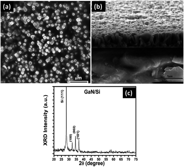 |
| | Fig. 1 (a) top-view, (b) cross-sectional view of FESEM images, and (c) XRD pattern of the GaN NRs grown on Si substrate by CVD. | |
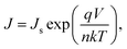
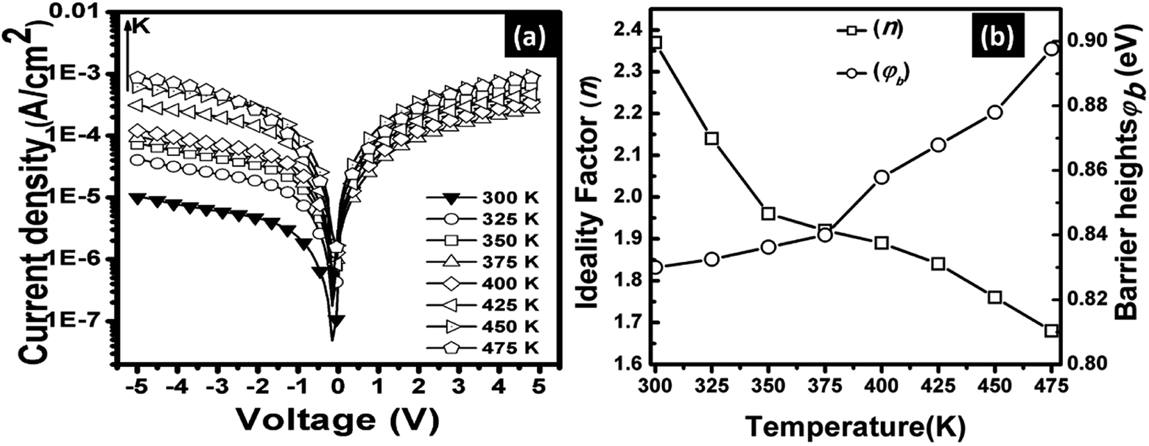
The electrical characteristics of the grown n-GaN NRs/p-Si heterojunction were monitored as a function of forward and reverse bias voltage conditions at 300–475 K. Fig. 2a shows I–V curves of the heterojunction device measured at different temperatures, indicating temperature-dependent behavior, which can be ascribed to the inhomogeneities at the interface.16,18 The current increases with increasing temperature due to the increase of the thermally-activated carriers and the reduction of the internal resistance. At high temperature, the rectifying nature deteriorates, possibly owing to the thermally-generated carrier tunneling.17,18 A slight decrease in the forward current at a higher temperature of 475 K was also observed. This behavior can be ascribed to the pronounced diffusion current at high bias voltage arising from the linear reduction in the barrier for electron and hole diffusion current. According to Einstein's relation, the diffusion current is strongly dependent on the carrier mobility.18 However, at higher temperatures, the phonon population increases resulting in decreased mobility. However, at a certain bias, an increase in temperature results in an increase in the forward current, an indicator that the current could be caused by the thermionic emission (TE). Thus, the current transport through a heterojunction at a forward bias can be understood based on the TE theory.26 The forward bias I–V measurements of the GaN/p-Si heterojunction can be given by eqn (1) and (2):26,27
| |
 | (1) |
| |
 | (2) |
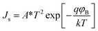
where
q is the electronic charge,
V is the applied forward bias voltage,
k is the Boltzmann's constant,
T is the absolute temperature,
n is the diode ideality factor,
A is the contact area,
Js is the reverse-bias saturation density current,
ϕB0 is the zero-bias barrier heights (BHs) of device, and
A* is the effective Richardson constant (
A* = 26.4 A cm
−2 K
−2 for n-GaN and 32 A cm
−2 K
−2 for p-Si).
16,28 The values of BHs and the ideality factor (
n) for the fabricated heterojunction were calculated as a function of temperature as extracted from the forward bias
I–
V curves. Both the saturation current density (
Js) and
n were estimated from the linear regions of the semi-log forward bias
I–
V curve according to
eqn (3):
26| |
 | (3) |
Upon plotting (ln
![[thin space (1/6-em)]](https://www.rsc.org/images/entities/char_2009.gif) J
J) against voltage, the slope gives the
n and the intercept gives the
Js. The obtained value of
Js is used to determine the zero bias BHs (
ϕB0):
26| |
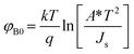 | (4) |
 |
| | Fig. 2 (a) Temperature-dependent J–V semi log plot for n-GaN/p-Si heterojunction and (b) the variations of ideality factor and barrier height as a function of temperature obtained from TE for GaN/Si heterojunction. | |
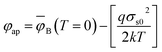
The zero bias BHs and n of the fabricated n-GaN/p-Si heterojunction diode were estimated at each temperature, as shown in Fig. 2b. It was observed that the BHs increase from 0.83 eV at 300 K to 0.90 eV at 475 K. As the temperature increases, more electrons would have sufficient energy to surmount the higher barrier. As a result, the dominant barrier height would increase with temperature.29 It was also observed that n deviates from unity and decreases with increasing temperature, which suggests the presence of an inhomogeneous barrier. The high values of n can be attributed to a wide distribution of low-Schottky barrier height (SBH) areas, tunneling through the interfacial layer, and a barrier inhomogeneities.20 Note that the dependence of ϕB and n on the temperature can be attributed to the heterogeneous and potential fluctuation at the interface.16,18,30 The BHs are possibly a function of the atomic inhomogeneities at the GaN/Si interfaces and the interface atomic structure, which are caused by nonuniformity of the interfacial charges, defects, and interfacial oxide layer composition.16 Consequently, the inhomogeneous BH may be varied as a result of the different types of defects that might exist at the GaN/Si interface. These observations are consistent with the TE theory and reported studies InGaN/Si barrier height17,21 and GaN/Si heterojunctions.11,20,23 However, in cases where the ideality factor is larger than unity, the TE would not be the only factor that promotes the transfer of current. As the BH depends on the applied voltage and, consequently, on the current flow across the interface, it is requisite to consider the standard field conditions. The electric field is zero across the interface under flat band (FB) conditions.
To extract more details on the barrier height, the flat band barrier height (FBBH) can be obtained from the J–V graphs, which is derived from the zero-bias barrier height (ϕB0) viaeqn (5) and (6):26
| | |
ϕBF = nϕB0 − (n − 1)(EF − EV)
| (5) |
| |
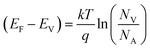 | (6) |
where
ϕBF is the flat-band barrier height,
EF is the Fermi energy,
EV is the valence band energy,
NV the effective density of states of the valence band, and
NA is the carrier concentration. Hall measurements revealed that the carrier density of the Si substrate was ∼6 × 10
19 cm
−3 (p-Si). Notably, the deposition of the GaN layer formation causes the surface of the Si substrate to become heavily p-type doped through Ga in-diffusion.
5 The GaN NRs layer is thought to have n-type behavior because of the
N vacancies or/and oxygen contamination during the growth process.
5,31 The FBBH was derived based on the assumption that the electron effective mass and
NA (the carrier concentration obtained from Hall measurement) do not vary with temperature. While the effective density of states in the valence band (
NV) will change with the temperature and is given by
eqn (7):
| |
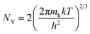 | (7) |
where
mh is the effective mass of hole (
mh/
mo = 0.56 for p-Si),
T is the absolute temperature, and
h is the Planck's constant. The relation can be written as
NV (cm
−3) = 4.3 × 10
14(
T)
3/2 for p-type Si.
32Fig. 3a shows the FBBHs as a function of temperatures. One can observe that the
ϕBF slightly decreases with increasing temperature, whereas the zero-bias (ZB) BHs increase with increasing temperature. The difference between the ZB and the FBH values suggests low inhomogeneity and potential fluctuation at the interface.
18,19 Futhermore, the temperature dependence of the
ϕBF can be defined by
eqn (8):
| | |
ϕBF = ϕBF(T = 0) + Tα
| (8) |
where
ϕBF (
T = 0) is the barrier height extrapolated to zero-temperature, and
α is the temperature cofficient of
ϕBF(
T). The values of
ϕBF(
T = 0) and
α have been extracted fom the intercept and slope according to
eqn (8). From the fit of the plot, the calculated values of
ϕBF(
T = 0) and
α were ∼2.5 eV and 0.0023 eV K
−1, respectively. The value of
ϕBF(
T = 0) is larger, which can be ascribed to the series resistance.
33 Also, the value of average barrier height
![[small phi variant, Greek, macron]](https://www.rsc.org/images/entities/i_char_e0d7.gif) B
B is lower than the
ϕBF(
T = 0), and can be explained by lateral inhomogeneities of barrier heights.
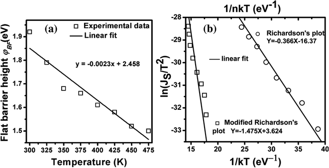 |
| | Fig. 3 (a) Variation of flat band barrier heights as a function of temperature for n-GaN/p-Si heterojunction and (b) conventional Richardson plot, lnIs/T2vs. 1/kT and “modified” Richardson's plot lnIs/T2vs. 1/nkT for the fabricated heterojunction. | |
Another method to extract the BH is through the application of a Richardson plot. From the experimental data measured in Fig. 2, the values of the saturation current (Js) were calculated at each temperature, and a “conventional” Richardson's plot, lnIs/T2versus 1/kT, is plotted as shown in Fig. 3b. From Richardson's plot, the barrier height and Richardson's constant were determined from the slope and intercept, respectively, using eqn (9):26,27
| |
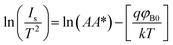 | (9) |
From this linear fit, the BH and the conventional Richardson's constant were 0.366 eV and 8.76 × 10⁻⁸ A cm−2 K−2, respectively. The obtained Richardson's constant is eight orders of magnitude smaller than the theoretical value of A* for p-Si.32 This deviation in A* is generally explained by the barrier inhomogeneity of the contacts, which means that it consists of high and low barrier areas at the interface.34 The inhomogeneous BH probably arises due to several types of defects present at the GaN NRs/Si hetero-interfaces.35 In addition, the effective area for current conduction (Aeff) is significantly lower than the geometric contact area (Ageom) due to the preferential current flow through the lower barrier height regions.18 In order to account for the temperature dependent n and BH, the modified Richardson's plot of ln(Is/T2) versus 1/nkT as proposed by Hackam and Harrop36 is shown in Fig. 3b. From the linear fit of the plot, the effective BH(ϕB0) and modified Richardson's constant were determined from the slope and intercept, respectively. The values of effective ϕB0 and the Richardson's constant A* were 1.475 eV and 37.48 A cm−2 K−2, respectively. The value of A* was eight orders of magnitude higher than that obtained from the conventional Richardson's plot. However, the value of A* obtained from the modified Richardson plot was found to be closer to the theoretical value for p-Si.11,32
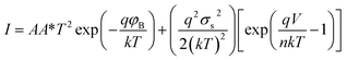
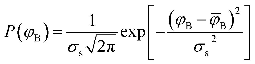
The other method is to use the Gaussian statistics (GS) to modify the conventional Richardson plot to determine the BHs, taking into account SBH lowering due to an inhomogeneous contact.37 This method uses GS to relate experimental values of BH extracted from I–V measurements. Using eqn (1) for current over the barrier ϕB allows the values of BH calculated from the I–V data to be plotted against the inverse thermal energy to extractthe standard deviation (σs) and mean BH B, which can be given by eqn (10):26
| |
 | (10) |
where

is the normalization constant of the Gaussian barrier height distribution. The total current
I(
V) across a heterojunction diode containing barrier inhomogeneities is expressed by
eqn (11):
37| |
 | (11) |
where
I(
ϕB,
V) is the current at a bias
V for a barrier of height based on the ideal thermionic emission diffusion (TED) theory and
P(
ϕB) is the normalized distribution function giving the probability of accuracy for barrier height. Solving the
eqn (1) and
(2), the total forward current can be given by
eqn (12):
26,27,38| |
 | (12) |
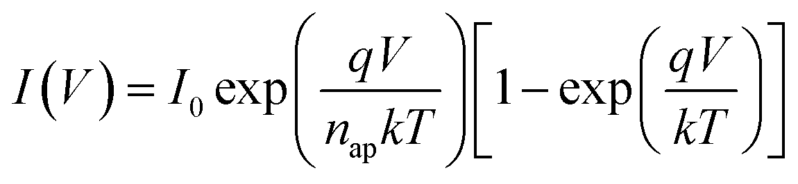
Applying the above integration (Eq.(11)), the current I(V) can be derived through a Schottky barrier at a forward bias but with a modified barrier as:38
| |
 | (13) |
where
ϕap and
nap are the apparent barrier height at zero bias and apparent ideality factor, respectively, and can be resolved by
eqn (14) and
(15):
37,38| |
 | (14) |
| |
 | (15) |
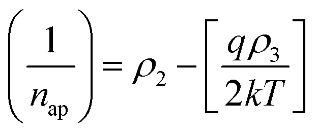
The mean BH (
B) and standard deviation (
σs) are assumed to be linearly bias-dependent on Gaussian parameters. The values of
B and
σs can be expressed as:
ϕB =
ϕB0 (
T = 0) +
ρ2V and
σs =
σs0 +
ρ3V, where
ρ2 and
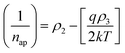
ρ3 are voltage coefficients, which may depend on temperature. The voltage coefficients quantify the voltage deformation of the barrier height distribution.
38 The value of
σs is usually very small therefore, can be ignored.
39 Verification of
σs0 and
ϕB0 values can be carried out using a modified Richardson plot.
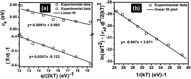
Fig. 4a shows the zero-bias apparent barrier heights extracted from
I–
V analysis plotted against the
q/2
kT and ideality factor
versus q/2
kT according to the Gaussian distribution (GD) of the BHs. The plot of
ϕBversus q/2
kT should be a straight line. The values of
σs0, and
B were extracted from the slope and intercept and found to be 0.0091 V and 0.993 eV, respectively. However, the voltage coefficients
ρ2 and
ρ3, which can be extracted from (1/
n) − 1
versus q/2
kT, were also reported in
Fig. 4. From the intercept and slope of the linear fit, voltage coefficients
ρ2 of 0.123 and
ρ3 of 0.025 eV were obtained. The linear behavior plot shows that the ideality factor expresses the voltage deformation of the GD of the SB contact. The structure with the best rectifying performance presents the best barrier homogeneity with the lower value of the standard deviation.
 |
| | Fig. 4 (a) The zero-bias apparent barrier heights extracted from I–V analysis plotted against the q/2kT and ideality factor versus q/2kT according to the GD of the BHs and (b) the modified Richardson plots ln(Is/T2) − 0.5σ2q2/(kT)2vs. 1/kT according to the GD of the BHs. | |
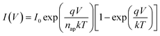
Verification of σs0 and ϕB0 values can be carried out using a modified Richardson plot. The Richardson plot can be modified by combining eqn (2), (14) and (15) such that:
| |
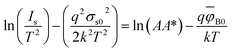 | (16) |
Fig. 4b shows the modified Richardson's plot of ln(Is/T2) − σs02q2/2(kT)2versus 1/kT. From the slope and the intercept of the modified plot, the mean B0 and modified Richardson's were extracted. The value of mean B0 obtained is 0.95 eV. Also, using eqn (2), the intercept (= lnAA*) at the ordinate determined A* for a given diode area (i.e. A ∼ 1 cm2) as 39.25 A cm−2 K−2. From the modified Richardson's plot and according to eqn (16), the obtained value of ϕB0 = 0.95 eV is consistant with that of ϕB0 = 0.99 eV extracted from the plot in Fig. 3a and lower than that of ϕB0 = 1.475 eV from Fig. 3b. Furthermore, the barrier heights (0.99 and 0.95 eV) are closely similar to the conduction band offset of GaN/Si heterojunction (0.95 eV), which renounces the thermally generated carrier tunneling.20 The preceding results confirm that predominant current transport is not the only method for ascertaining barrier height inhomogeneities (BHI) in GaN/Si heterojunction sample. The results also establish that Gaussian distributions (GD) of BHs and modified Richardson for GD of BHs are also applicable. Table 1 summarizes the obtained values of BHs and Richardson's constant according to the modified Richardson's plot, GD of BHs, and modified GD of BHs methods. The values of BHs and Richardson constant, which were extracted using the modified Richardson's GD of BHs, are more acceptable. The outcome also concurs with the theoretical values.
Table 1 The values of BHs and Richardson constant of the fabricated GaN/Si heterojunction
| Methode |
BHs (eV) |
Richardson constant (A cm−2 K−2) |
| Modified Richardson's plot |
1.475 |
37.48 |
| GD of BHs |
0.99 |
— |
| Modified GD of BHs |
0.95 |
39.25 |
Fig. 5 shows the possible band alignment diagram of n-GaN/p-Si heterojunction. The bandgaps (Eg) and electron affinities (χ) used are Eg(Si) = 1.12 eV, χ(Si) = 4.05 eV, Eg(GaN) = 3.4 eV, and χ(GaN) = 3.1 eV, respectively, hence the conduction band offset (ΔEC = χ(GaN) − χ(Si)) is 0.95 eV, which is much smaller than the valence band offset, i.e., ΔEV = ΔEg − ΔEC = (1.33 eV).35,39
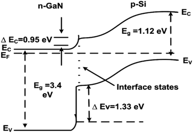 |
| | Fig. 5 Schematic energy band alignment diagram of the n-GaN/p-Si heterojunction under thermal equilibrium. | |
4. Conclusions
In conclusion, a high-quality n-GaN NRs/p-Si heterojunction device has been successfully fabricated. The relatively sharp diffraction peaks in the XRD spectra indicated the growth of highly crystalline GaN nanorods with wurtzite structure. The temperature dependence of the I–V characteristics of the fabricated heterojunction has been discussed. Using the TE model, the ideality factor (n) and barrier height (BH) of the heterojunction device were determined from the forward I–V curves under dark conditions. It is found that the values of ideality factor decreases with increasing the temperature, which suggests the presence of an inhomogeneous barrier. Deviations of n from unity reveal that TE will not be the only way that promotes the current transfer. It is observed that the ϕBF slightly decreases with increasing temperature, whereas the zero-bias (ZB) BHs increase with temperature. We have obtained a temperature coefficient BH of (α = 2.3 meV K−1) for this heterojunction. The measured value of the effective barrier height (∼1.48 eV) via the modified Richardson's plot is larger than that of BHs of 0.99 eV and 0.95 eV obtained by GD and modified Richardson GD, respectively. The calculated values of BHs and Richardson constant, which were extracted from the modified Richardson's GD of BHs, are reasonably acceptable.
Data availability statement
The data that supports the findings of this study are available upon request.
Conflicts of interest
There are no conflicts to declare.
References
- R. Quai, Gallium nitride electronics, Springer Verlag, Berlin, Heidelberg, 2008 Search PubMed.
- M. A. Qaeed, K. Ibrahim, K. M. A. Saron, M. A. Ahmed and N. K. Allam, Low-temperature solution-processed flexible solar cells based on (In, Ga) N nanocubes, ACS Appl. Mater. Interfaces, 2014, 6, 9925–9931 CrossRef CAS.
- C. M. Yang, D. S. Kim, S. G. Lee, J. H. Lee, Y. S. Lee and J. H. LEE, Improvement in electrical and optical performances of GaN-Based LED with SiO2/Al2O3 double dielectric stack layer, IEEE Electron Device Lett., 2012, 33(4), 564–566 CAS.
- M. Manikandan, D. Nirmal, J. Ajayan, P. Mohankumar, P. Prajoon and L. Arivazhagan, A review of blue light emitting diodes for future solid state lighting and visible light communication applications, Superlattice. Microst., 2019, 136, 106294 CrossRef CAS.
- K. M. A. Saron, M. R. Hashim and N. K. Allam, Heteroepitaxial growth of GaN/Si (111) junctions in ammonia-free atmosphere: Charge transport, optoelectronic, and photovoltaic properties, J. Appl. Phys., 2013, 113, 24304 CrossRef.
- Z. A. Syed, Y. Hou, X. Yu, S. Shen, M. Athanasiou, J. Bai and T. Wang, Ultra-energy-efficient photoelectrode using microstriped GaN on Si, ACS Photonics, 2019, 6, 1302–1306 CrossRef CAS.
- K. M. A. Saron, M. R. Hashim, N. Naderi and N. K. Allam, Interface properties determined the performance of thermally grown GaN/Si heterojunction solar cells, Sol. Energy, 2013, 98, 485–491 CrossRef CAS.
- Z. Yang, F. Guarin, I. W. Tao and W. I. Wang, Approach to obtain high quality GaN on Si and SiC on silicon-on-insulator compliant substrate by molecular-beam epitaxy, J. Vac. Sci. Technol., B, 1995, 13, 789–791 CrossRef CAS.
- A. Tanaka, W. Choi, R. Chen, R. Liu, W. M. Mook, K. L. Jungjohann, P. K. L. Yu and S. A. Dayeh, Structural and electrical characterization of thick GaN layers on Si, GaN, and engineered substrates, J. Appl. Phys., 2019, 125, 082517 CrossRef.
- Y. Li, W. Wang, X. Li, L. Huang, Z. Lin, Y. Zheng, X. Chen and G. Li, Stress and dislocation control of GaN epitaxial films grown on Si substrates and their application in high-performance light-emitting diodes, J. Alloys Compd., 2019, 771, 1000–1008 CrossRef CAS.
- T. N. Bhat, M. K. Rajpalke, B. Roul, M. Kumar and S. B. Krupanidhi, Substrate nitridation induced modulations in transport properties of wurtzite GaN/p-Si (100) heterojunctions grown by molecular beam epitaxy, J. Appl. Phys., 2011, 110, 093718 CrossRef.
- A. Szyszka, M. Wosko, B. Paszkiewicz and R. Paszkiewicz, Surface electrical characterization of defect related inhomogeneities of AlGaN/GaN/Si heterostructures using scanning capacitance microscopy, Mater. Sci. Semicond. Process., 2019, 94, 57–63 CrossRef CAS.
- H. Iguchi, T. Narita, K. Kataoka, M. Kanechika and A. Uedono, Impact of defects on the electrical properties of p–n diodes formed by implanting Mg and H ions into N-polar GaN, J. Appl. Phys., 2019, 126, 125102 CrossRef.
- B. Roul, M. Kumar, M. K. Rajpalke, T. N. Bhat, N. Sinha, A. Kalghatgi and S. Krupanidhi, Effect of N/Ga flux ratio on transport behavior of Pt/GaN Schottky diodes, J. Appl. Phys., 2011, 110, 064502 CrossRef.
- F. Roccaforte, F. Giannazzoa, A. Alberti, M. Spera, M. Cannas, I. Cora, B. Pecz, F. Iucolano and G. Greco, Barrier inhomogeneity in vertical Schottky diodes on free standing gallium nitride, Mater. Sci. Semicond. Process., 2019, 94, 164–170 CrossRef CAS.
- F. Iucolano, F. Roccaforte, F. Giannazzo and V. Raineri, Barrier inhomogeneity and electrical properties of Pt/GaN Schottky contacts, J. Appl. Phys., 2007, 102, 113701 CrossRef.
- T. T. A. Tuan, D. H. Kuo, K. Lin and G. Z. Li, Temperature dependence of electrical characteristics of n-InxGa1-xN/p-Si hetero-junctions made totally by RF magnetron sputtering, Thin Solid Films, 2015, 589, 182–187 CrossRef CAS.
- T. N. Bhat, B. Roul, M. K. Rajpalke, M. Kumar, S. B. Krupanidhi and N. Sinha, Temperature dependent transport behavior of n-InN nanodot/p-Si heterojunction structures, Appl. Phys. Lett., 2010, 97, 202107 CrossRef.
- Y. Zhou, D. Wang, C. Ahyi, C.-C. Tin, J. Williams, M. Park, N. M. Williams, A. Hanser and E. A. Preble, Temperature-dependent electrical characteristics of bulk GaN Schottky rectifier, J. Appl. Phys., 2007, 101, 024506 CrossRef.
- L. Mohan, G. Chandan, S. Mukundan, B. Roul and S. B. Krupanidhi, Double Gaussian distribution of barrier height observed in densely packed GaN nanorods over Si (111) heterostructures, J. Appl. Phys., 2014, 116, 234508 CrossRef.
- M. Kumar, B. Roul, M. K. Rajpalke, T. N. Bhat, A. T. Kalghatgi and S. B. Krupanidhi, Electrical transport studies of MBE grown InGaN/Si isotype heterojunctions, Curr. Appl. Phys., 2013, 13, 26–30 CrossRef.
- K. P. Hsueh, Y. H. Cheng, H. Y. Wang, Y. Peng, H. C. Wang, H. C. Chiu, C. W. Hu and R. Xuan, Effect of AlN spacer layer thickness on AlGaN/GaN/Si Schottky barrier diodes, Mater. Sci. Semicond. Process., 2017, 66, 69–73 CrossRef CAS.
- Z. Xu, L. Zhang, H. He, J. Wang and M. Xie, Growth of GaN on Si (111): Surfaces and crystallinity of the epifilms and the transport behavior of GaN/Si heterojunctions, J. Appl. Phys., 2011, 110, 093514 CrossRef.
- T. T. A. Tuan, D.-H. Kuo, P. T. Cao, V. S. Nguyen, Q.-P. Pham, V. K. Nghi and N. P. L. Tran, Electrical Characterization of RF Reactive Sputtered p-Mg-InxGa1−xN/n-Si Hetero-Junction Diodes without Using Buffer Layer, Coatings, 2019, 9, 699 CrossRef CAS.
- K. M. A. Saron and M. R. Hashim, Study of using aqueous NH3 on synthesizes GaN nanowires on Si (111) by thermal chemical vapor deposition, Mater. Sci. Eng. B, 2013, 178, 330–335 CrossRef CAS.
- S. M. Sze and K. K. Ng, Physics of semiconductor devices: 1981New York Search PubMed.
- D. A. Neamen, Semiconductor physics and devices: basic principles, Richard D: Irwin, Boston, 1992 Search PubMed.
- S. Chand and J. Kumar, Evidence for the double distribution of barrier heights in Pd2Si/n-Si Schottky diodes from I-V-T measurements, Semicond. Sci. Technol., 1996, 11, 1203–1208 CrossRef CAS.
- H. Hasegawa, T. Sato and T. Hashizume, Evolution mechanism of nearly pinning-free platinum/n-type indium phosphide interface with a high Schottky barrier height by in situ electrochemical process, J. Vac. Sci. Technol., B, 1997, 15, 1227–1235 CrossRef CAS.
- M. Kumar, B. Roul, T. N. Bhat, M. K. Rajpalke, A. Kalghatgi and S. Krupanidhi, Carrier transport studies of III-nitride/Si3N4/Si isotype heterojunctions, Phys. Status Solidi A, 2012, 209, 994–997 CrossRef CAS.
- S. Strite and H. Morkoc, GaN, AlN, and InN: a review, J. Vac. Sci. Technol., B, 1992, 10, 1237–1266 CrossRef CAS.
- W. Shockley, Electrons and holes in semiconductors, van Nostrand, 1963 Search PubMed.
- M. A. Hamdy and R. L. Call, The effect of the diode ideality factor on the experimental determination of series resistance of Solar Cells, Sol. Cell., 1987, 20, 119–126 CrossRef CAS.
- J. M. Dhimmar, H. N. Desai and B. P. Modi, Analysis of the Inhomogeneous Barrier in In/p-Si Schottky Contact and Modified Richardson Plot, J. Nano- Electron. Phys., 2016, 8, 02006 Search PubMed.
- B. Roul, M. Kumar, M. K Rajpalke, T. N. Bhat and S. B. Krupanidhi, Binary group III-nitride based heterostructures: band offsets and transport properties, J. Phys. D: Appl. Phys., 2015, 48, 423001 CrossRef.
- R. Hackam and P. Harrop, Electrical properties of nickel-low Doped n-type gallium arsenide Schottky-barrier diodes, IEEE Trans. Electron Devices, 1972, 19, 1231–1238 CAS.
- J. H. Werner and H. H. Guttler, Barrier inhomogeneities at Schottky contacts, J. Appl. Phys., 1991, 69, 1522–1533 CrossRef CAS.
- M. Kumar, B. Roul, T. N. Bhat, M. K. Rajpalke, A. Kalghatgi and S. Krupanidhi, Barrier inhomogeneity and electrical properties of InN nanodots/Si heterojunction diodes, J. Nanomater., 2011, 2011, 1–7 Search PubMed.
- T. Cook, C. Fulton, W. Mecouch, R. Davis, G. Lucovsky and R. Nemanich, Band offset measurements of the Si3N4/GaN (0001) interface, J. Appl. Phys., 2003, 94, 3949–3954 CrossRef CAS.
|
| This journal is © The Royal Society of Chemistry 2020 |
Click here to see how this site uses Cookies. View our privacy policy here. 
 Open Access Article
 This Open Access Article is licensed under a
  *e
*e


 is the normalization constant of the Gaussian barrier height distribution. The total current I(V) across a heterojunction diode containing barrier inhomogeneities is expressed by eqn (11):37