
 Open Access Article
 This Open Access Article is licensed under a
 Creative Commons Attribution 3.0 Unported Licence
Visible region absorption in TMDs/phosphorene heterostructures for use in solar energy conversion applications
Ashraf Maniyar * and
Sudhanshu Choudhary
* and
Sudhanshu Choudhary
National Institute of Technology, Kurukshetra, India. E-mail: ashrafchand14@gmail.com; hellosudhanshubit@gmail.com; sudhanshu@nitkkr.ac.in; Tel: +917206550867
First published on 26th August 2020
Abstract
Heterostructures of pristine black phosphorene (P) with transition metal dichalcogenides (TMDs) monolayers of MoS2, MoSe2, MoTe2, WS2, and WSe2 are investigated using density functional theory based simulations. The results suggest that individual MoS2, MoSe2, MoTe2, WS2, WSe2, and black phosphorene have high absorption in some portions of the visible region (∼390–430 nm) and in the entire ultraviolet (UV) region. All the heterostructures results into redshift phenomena where absorption peaks are seen to shift to lower energies of the spectrum. The absorption coefficient is seen to increase with the wavelength and appears to be shifted towards the red end of the spectrum. High absorption is also observed in the entire visible region (λ ∼ 410 to 780 nm) of the spectrum for all heterostructures. This high absorption in the desired visible range may find many potential applications for the heterostructure, such as in the fabrication of optoelectronic devices and solar cells. The refractive index and dielectric constant of the heterostructure are also calculated and are found to be in line with trends in dielectric constant. Furthermore, it is observed that most of the resultant heterostructures have type-II band alignment which is ideal for solar energy conversion and optoelectronic applications.
I. Introduction
Two-dimensional (2D) monolayer graphene which was experimentally discovered in 2004, has created huge interest among researchers for conducting more studies on 2D nanomaterials as they possess distinctive physical and chemical properties which can be used in various applications in the field of optoelectronics and nanoelectronics.1–6 Since then, other two dimensional materials that have unique properties have been explored such as germanene,7 silicine,8 phosphorene9 and transition metal dichalcogenides (TMDs) like MoS2, MoTe2, MoSe2, WS2, and WSe2.10 These layered 2D substance have many of the properties of graphene and find use in electronic devices. For example, to design an excessive performance field-effect-transistor (FET), germanene is usually used inside the device channel. Due to its novel electronic characteristics, hexagonal boron nitride (h-BN) presents a perfect 2-D structural copy of graphene and because of its large insulator type bandgap of ∼6.3 eV it acts as a terrific dielectric substrate.11 However, the insignificant bandgap of graphene limits its use in optical applications and hence we focus our interest on TMDs. Phosphorene is flexible like graphene and it can be mechanically desquamated. Graphene is rarely used in optoelectronic applications due to the absence of a bandgap whereas, monolayers of all TMDs have indirect or direct bandgaps that can be tuned by varying the number of layers which makes TMDs an ideal material for optoelectronic applications.12–15While there exist many single and bilayer materials with weak van-der-Waals interaction between the layers and strong in-plane covalent bonds.16 Materials like TMDs (MoS2, MoSe2, MoTe2, WS2, and WSe2) have received a remarkable interest because of their unique optical and electronic properties. It is a known fact that the bandgap changes (from indirect to direct) when a single layer is exfoliated from a bilayer material.17 TMDs are also composed of van-der-Waals bonded X–Mo–X and X–W–S (X = S, Se, Te) units like graphene.18–20 To obtain ultrathin crystals of TMDs, a micromechanical cleavage technique can be used, as the bonds between two different layers in MoS2, MoSe2, MoTe2, WS2, and WSe2 crystals are very weak whereas it has strong interlayer interaction.21 Previous research works have suggested that the properties of MoS2, MoSe2, MoTe2, WS2, and WSe2 can be tuned by varying the number of layers12,13 and can thus find application the field-effect transistors and optoelectronic devices.17,21–25
Optical absorption in heterostructures consisting of atomically thin TMDs strongly depend on the phase, structure and thickness of the TMD layers.26 The dispersion energy, optical spectra moments and the dielectric constant were all found to decrease with increase in SnS thin film's thicknesses.27 The number of layers (thickness) can manipulate the electronic properties of Mo and W based TMDs, where an increase in bandgap was observed with decrease in thickness from bulk to monolayers.28 Energy gap and refractive index were reported to vary with thickness of CdI2 films in ref. 29. An increase in refractive index with thickness of CdSe thin films was reported in ref. 30. In ref. 31 a blue shift in the optical bandgap was observed with respect to the bulk value on increasing the thickness of ZnO thin film deposited on Si. Dependence of optical properties on the thickness of amorphous Ge30Se70 thin films is investigated in ref. 32, where it was reported that increasing the film thickness increases the direct optical energy gap and decreases the refractive index. Heterostructures consisting of atomically thin TMDs exhibit excellent electronic and optoelectronic properties and great potential in optoelectronics and photovoltaics as optical absorption strongly depend on the phase structure and thickness of the TMDs layer. The single layers of TMDs can be used in the fabrication of high mobility FET.33 The TMD heterostructure with black phosphorene can show dramatic improvements in its optical properties. P–n diode photodetector made up of heterostructure of MoS2 and black phosphorene has shown high responsivity of 418 mA W−1, which is approximately 100 times more than the phototransistor of black phosphorus.34 MoS2 heterostructure with AlN and GaN have been suggested for ultra high effectiveness in the field of photocatalytic activity that can be useful for water splitting application.35,36
Phosphorene is a p-type semiconducting material which is abundantly available in nature and is a popular material.37 Monolayer phosphorene has unique material properties like graphene and MoS2, and it can be mechanically exfoliated.38 It has well-built physical anisotropy and high conductance that finds applications in the field of nano-electronics and optoelectronics.39 Not only multi-layered but single-layered black phosphorene have also been successfully exfoliated.9,40–42 Previous research works have shown that black phosphorene has good carrier mobility and has direct bandgap.43–45 Phosphorene has a puckered structure in which each phosphorus atom is bonded covalently with the other three atoms. Phosphorene material has turned into one of the most researched hotspots due to its excellent properties which can be used in optoelectronics and sensor applications.46–48
Nowadays, almost all the layered 2D materials have attracted the researchers because of their usefulness in optoelectronics and photonics applications, their heterostructures have shown outstanding optical properties. The fabrication of heterostructures are possible by stacking 2D materials technique.49 Two n-type monolayers of MoS2 stacked on P-type WSe2 forms a p–n junction in which type-II band alignment exists.50–52 Heterostructures of phosphorene with graphene and boron nitrides have been investigated using images obtained from scanning tunneling microscopy (STM).53 Wearable batteries, distinct types of energy harvesters and supercapacitors and other wearable energy sources based on 2D materials have been suggested in ref. 54. Moreover, heterostructures of MoS2-on-MXene can be accomplished in batteries that are made using Li-ion due to the enhanced Li2S and Li adsorption and associated metallic property.55
2D materials have different energy band structures and bandgaps. However, monolayers of MoS2, MoSe2, MoTe2, WS2, WSe2, and phosphorene have almost similar bandgap with similar hexagonal structure56 and are potential materials for light accumulation. Phosphorene has high carrier mobility, while MoS2, MoSe2, MoTe2, WS2, and WSe2 have high photo responsivity. It would be interesting to investigate their heterostructures that could display desired band alignment for ruling out the recombination of electron–hole pairs.
It is understood that there exist many studies on phosphorene/TMD heterostructures with type-II band alignment,20,34,42,56 however, most of them lack detail investigations on electronic and optical properties. Some of them have reported only the electronic structure with a small set of TMDs, and the others have reported only optical properties of blue phosphorene/TMD heterostructures. In this paper, we perform a detail investigation on the heterostructures of black phosphorene with all possible set of suitable TMDs and have included the results on binding energy calculations for experimental stability, band structure calculations for electronic property, and band alignments, refractive index, dielectric constant and absorption coefficient calculations for predicting optical properties. The results suggest that the absorption in black phosphorene can be tuned to higher levels due to red-shift or shifting of absorption peaks to lower energies in the black phosphorene/TMD heterostructure. It is found that MoS2/P MoSe2/P, MoTe2/P, WS2/P, and WSe2/P heterostructures result in large absorption in the visible and IR regions due to combined properties of MoS2, MoSe2, MoTe2, WS2, WSe2, and phosphorene. Potential applications of the heterostructures could be their use as photovoltaic materials. The resulting electronic properties also suggest that the heterostructures demonstrate type-II band alignments, hence constraining the photo-generated recombination of electron–hole pairs. The 2D and layered materials have considerable properties from their bulk crystals and find application in energy storage devices and electronics.57,58
II. Computational details
The optical as well as electronic properties are studied for MoS2/P, MoSe2/P, MoTe2/P, WS2/P, and WSe2/P heterostructures. Thickness of MoS2, MoSe2, MoTe2, WS2, WSe2 and phosphorene are 0.65 nm, 0.7 nm, 32 nm, 1 nm, 0.7 nm and 2.1 nm, respectively. Number of atoms in MoS2/P, MoSe2/P, MoTe2/P, WS2/P, WSe2/P heterostructures are 40, 20, 34, 20 and 20, respectively. Simulations were performed using first-principles method based on density functional theory (DFT) on Atomistix Tool Kit (ATK). The exchange-correlation energy of the system is approximated using generalized gradient approximation (GGA) of Perdew–Burke–Ernzerhof (PBE).59,60 For geometry relaxation of all atoms, LBFGS algorithm with force tolerance 0.05 eV Å−1 is used. Optimized structures are shown in Fig. 1. Brillouin-zone sampling with 9 × 9 × 1 k-points in x–y–z direction has been used, mesh cut-off energy is set as 150 Ry.50 Semi-empirical DFT-D2 Grimme method was used since standard PBE function cannot completely describe van der Waals (vdW) interactions.61 | ||
| Fig. 1 Optimized structures of (a) heterostructure of MoS2/P, (b) MoSe2/P, (c) MoTe2/P, (d) WS2/P, (e) WSe2/P, with their interlayer distances with phosphorene. | ||
For obtaining optical properties, DFT with meta-GGA is used with 15 × 15 × 1 k-point brillouin zone sampling as in ref. 62. Considering thermal effects on the optical properties of the structure, broadening is set as 0.05 eV.
The calculation of susceptibility tensor is performed with the help of Kubo–Greenwood equation as

For calculation of susceptibility, relative dielectric constant ‘εr’, response coefficients, optical conductivity ‘σ’, and polarizability ‘α’ are used as63
| εr = (1 +χ(ω)), |
| α(ω) = Vε0χ(ω), σ(ω) = −img(ωε0χ(ω)) |
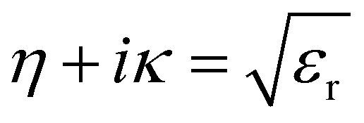
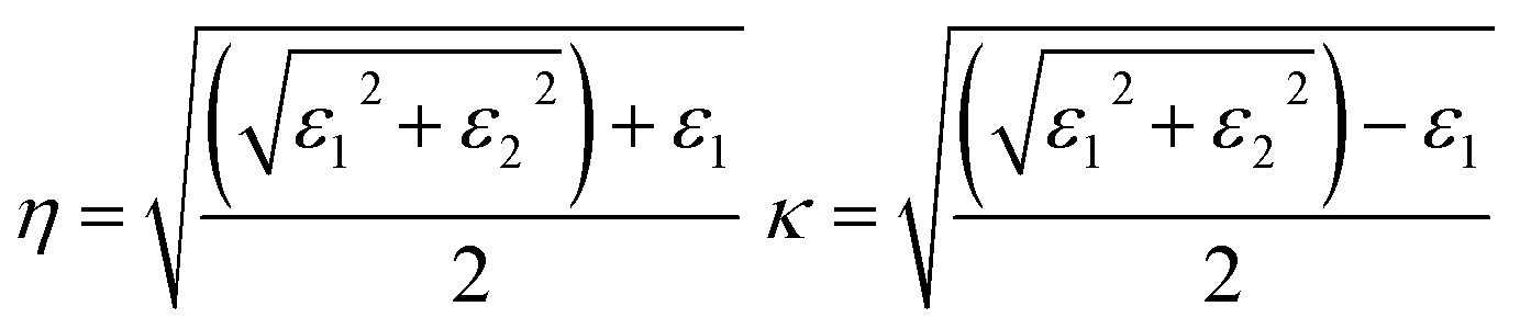
The refractive index η is defined in terms of εr and extinction coefficient κ as:
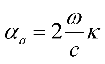
Coefficient of optical absorption is related to the extinction coefficient as64
III. Results and discussions
A. Geometric structure and stability
The structural parameters of monolayer MoS2, MoSe2, MoTe2, WS2, WSe2, and pristine black phosphorene are inspected to establish an appropriate heterostructure. Graphene has a planar structure,6 whereas, phosphorene has honeycomb puckered structure in the armchair (y-axis) and bilayer in the zig–zag (x-axis). The in-plane P–P bonds length is 2.22 Å and the interlayer bridge length is 2.24 Å. The in-plane bond angles are 96.34° and out of the plane bond angle is 102.09°. The MoS2, MoSe2, MoTe2, WS2, and WSe2 monolayers consist of weakly bonded S–Mo–S, Se–Mo–Se, Te–Mo–Te, S–W–S, and Se–W–Se structures, respectively. The in-plane lattice parameters are calculated as a = 3.16 Å for MoS2, a = 3.28 Å for MoSe2, a = 3.51 Å for MoTe2, a = 3.15 Å for Ws2, and a = 3.28 Å for WSe2, with γ = 120° which are in confirmation with other studies.17,40The optimized heterostructures are shown in Fig. 1, which are developed in a way that produces minimum lattice mismatch. The lattice mismatch values obtained for the heterostructures are 3.69%, 3.32%, 3.48%, 3.33%, 3.79% for MoS2, MoSe2, MoTe2, WS2, and WSe2 heterostructures, respectively, in Fig. 1. Such small values of lattice mismatch indicates that the total strains will lead to moderately small effects on the electronic structure of the heterostructures.
The binding energy at the heterostructure interface is calculated for obtaining the most stable configuration of the heterostructure. The binding energy at the interface is defined as EB = {E − (E1 + E2)}/N, where E is the total energies of MoS2/P, MoSe2/P, MoTe2/P, WS2/P, and WSe2/P heterostructure, E1 is the total energy of free-standing MoS2, MoSe2, MoTe2, WS2, WSe2, and E2 is the total energy of phosphorene monolayer. N represents the total number of atoms in the heterostructure.65 The calculated binding energies of the heterostructures versus interlayer distance between the monolayers of MoS2, MoSe2, MoTe2, WS2, WSe2, and phosphorene are shown in Fig. 2.
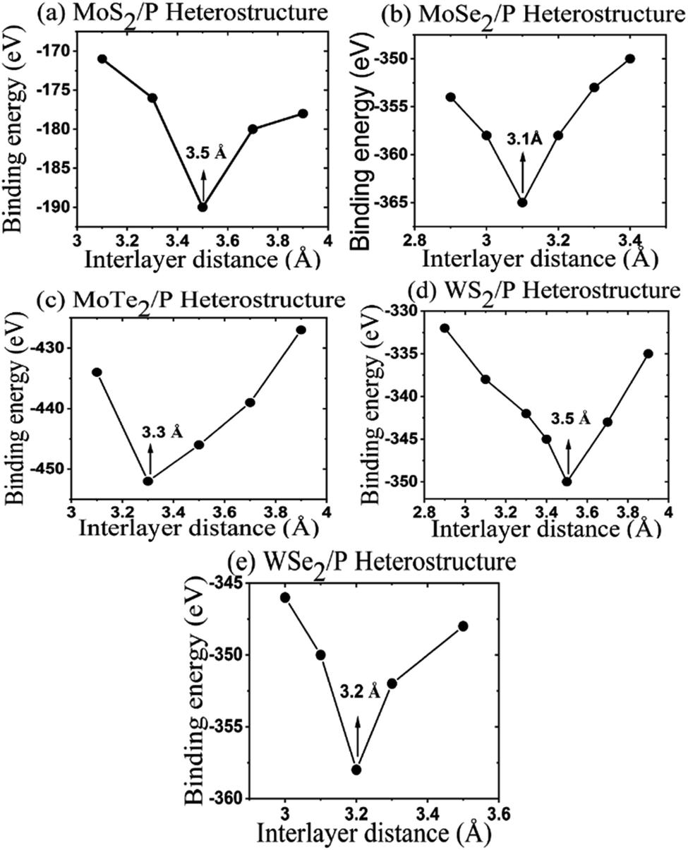 | ||
| Fig. 2 Graph of binding energy vs. the distance of interlayer. | ||
For obtaining stable configurations of heterostructure, binding energies of the structures should be negative, which is obtained in Fig. 2 for all the considered heterostructures. The interlayer gap at equilibrium for MoS2/P, MoSe2/P, MoTe2/P, WS2/P, and WSe2/P are calculated as 3.5 Å, 3.1 Å, 3.3 Å, 3.5 Å, 3.2 Å, respectively with per atom binding energy of about 6820.934 eV, 7096.603 eV, 14![[thin space (1/6-em)]](https://www.rsc.org/images/entities/char_2009.gif) 522.7597 eV, 6647.294 eV, and 6925.11452 eV respectively. Such values of binding energies shows that resultant heterostructures have strong van der Waals interaction.
522.7597 eV, 6647.294 eV, and 6925.11452 eV respectively. Such values of binding energies shows that resultant heterostructures have strong van der Waals interaction.
B. Optical properties
The optical properties and dielectric constant of the TMD heterostructures are evaluated. The performance of the dielectric material in terms of the electric energy storage is expressed by its dielectric constant (ε). The behavior of incident light when passing through a material is defined by its dielectric constant.The polarization and abnormal dispersion effects are resolved by the real part of dielectric constant, while neutral charge excitation oriented energy absorption in a system is measured by the imaginary part. Fig. 3 shows the imaginary (ε2) components of the calculated dielectric function as part of photon energy along XX, YY and ZZ directions for the heterostructures.
 | ||
| Fig. 3 Imaginary parts of dielectric constant along the XX, YY and ZZ tensors as a function of energy for TMDs and their heterostructures with phosphorene. (a) MoS2 (c) MoSe2, (e) MoTe2, (g) WS2 and (i) WSe2. Heterostructures of (b) MoS2/P, (d) MpSe2/P, (f) MoTe2/P, (h) WS2/P and (j) WSe2/P. Dielectric function of phosphorene is shown in (k). | ||
For finding the optical absorption of 2D materials, the dielectric function's imaginary part (ε2) is an important parameter, thus we consider only the curves of ε2 in y-direction, whereas the results of remaining two directions can be deduced from the same.66 In Fig. 3, for MoS2 monolayer, there are two peaks: the strongest at ∼2.5 eV and the sub-strongest at ∼1.8 eV.
Similarly, dielectric peaks for other TMD monolayers can be observed in Fig. 3. For pristine phosphorene, most of the peaks are in the range of 2.5–4.0 eV with the strongest peak appearing at ∼3 eV. The peaks in absorption coefficient in Fig. 4 are in course with peaks in dielectric function. These range of dielectric function values obtained for MoS2, MoSe2, MoTe2, WS2, WSe2 and phosphorene are matching the values reported in ref. 66 and 67. Whereas, for TMD heterostructures of MoS2/P, MoSe2/P, MoTe2/P, WS2/P, and WSe2/P, major peaks in the dielectric function are obtained in the region 0–2 eV, 1.5–4.5 eV, 1.5–2.5 eV, 2–4.5 eV, 1.5–4.5 eV, respectively.
 | ||
| Fig. 4 Absorption coefficient as a function of energy for (a) phosphorene, (c) MoS2, (g) MoSe2, (k) MoTe2 (o) WS2, (s) WSe2, and heterostructures of (e) MoS2/P, (i) MoSe2/P, (m) MoTe2/P, (q) WS2/P and (u) WSe2/P along the XX, YY and ZZ tensors. Absorption coefficient as a function of wavelength are also shown for (b) phosphorene, (d) MoS2, (h) MoSe2, (l) MoTe2, (p) WS2, (t) WSe2, and heterostructures of (f) MoS2/P, (j) MoSe2/P, (n) MoTe2/P, (r) WS2/P and (v) WSe2/P along the XX, YY and ZZ tensors. | ||
From Fig. 3 and 4, it can be observed that the dielectric and absorption edges for all the structures are matching their bandgaps in Fig. 6. In the absorption coefficient plot of Fig. 4, a shift in absorption edges towards lower energy range has been seen for the heterostructures. The existence of the redshift phenomenon can also be observed in all the heterostructures in comparison to absorption in pristine phosphorene. It can be observed from Fig. 4 that phosphorene has very high absorption peaks in the UV region (100–380 nm range), and here TMD based heterostructures have been investigated for tuning/shifting these absorption peaks of phosphorene from UV to visible (from left to right/from high energies to low energies) region or in other words shifting the absorption peaks from UV to red-end of the visible region in the spectrum (red-shift).
This shifting of absorption towards lower-energy (red-shift) is due to the fact that the heterostructures have a lower bandgap because of which the photo-generated electrons can be excited directly from the valence band of TMDs to the conduction band of phosphorene thereby resulting in larger absorption in the visible region. In heterostructures, peaks in refractive index also appear to shift towards lower energies in comparison to the peaks in phosphorene, which also justifies that more photons will be absorbed in the visible region or a resulting red-shift which is confirmed my absorption peaks in this region in Fig. 4. This means that the heterostructures would result in strong and stable absorption of light within the visible range in comparison to individual TMDs or phosphorene. The existence of shift phenomenon is a result of lower bandgap in the heterostructure due to which the conduction band of phosphorene is directly filled by the excited photo-generated electrons of the valence band of MoS2, MoSe2, MoTe2, WS2, and WSe2. Hence, it can be said that for visual light the heterostructure would display aggravated absorption.
Since dielectric constant is directly proportional to absorption coefficient, peaks in the dielectric function in Fig. 3 convert into the peaks in the absorption coefficient in Fig. 4. In MoS2, MoSe2, MoTe2, WS2, and WSe2, strongest peaks can be observed at around 2.5 eV, 2.4 eV, 2 eV, 3.8 eV and 5 eV, respectively. Whereas, there are two peaks located at around 3 eV and 3.8 eV for phosphorene. The dielectric constant values are in consistence with values of absorption coefficient. The heterostructure results in stable broader spectrum range of absorption in comparison to its constituent layers, which can be useful in optoelectronic applications.
Furthermore, it is noticed that in MoS2, MoSe2, MoTe2, WS2, and WSe2, YY and XX tensors overlap one another, while the ZZ tensor is free from overlapping. This implies anisotropic or isotropic behavior of monolayer MoS2, MoSe2, MoTe2, WS2, and WSe2, as in ref. 67. It is observed from Fig. 3–5 that the anisotropy property of phosphorene has been carried over in phosphorene based TMD heterostructures.
Refractive indexes (η) are computed from the dielectric functions for all the structures and are shown in Fig. 5. The peaks in refractive index follows the trends in both dielectric constant and absorption coefficient. The heterostructures of MoS2/P, MoSe2/P, MoTe2/P, WS2/P, and WSe2/P with their major peaks in the refractive index are obtained in the region 0–0.2 eV, 1.2–2.2 eV, 1.5–2.1 eV, 3.0–4.0 eV, and 0–0.2 eV, respectively. The peaks in refractive index in Fig. 5 for all the heterostructures corresponds to the peaks in dielectric constant in Fig. 3. The regions in Fig. 5 where refractive index is large would result in large absorption as it means light would stay for a longer time in these specific regions. Similarly, the portions where refractive index is small would result in lower absorption. The light is expected to stay longer in the systems with larger refractive index, resulting due to larger absorption of the photons in such systems. Lower absorption is observed in some regions, despite having high dielectric constant values in those regions. This reduction in absorption is due to lower values of refractive index in those regions, which is in agreement with the dielectric function (ε2) for the particular structures.
 | ||
| Fig. 5 Refractive index as a function of energy for (a) MoS2, (c) MoSe2, (e) MoTe2 (g) WS2, (i) WSe2 and (k) phosphorene. Refractive index of heterostructures of (b) MoS2/P, (d) MoSe2/P, (f) MoTe2/P, (h) WS2/P and (j) WSe2/P along the XX, YY and ZZ tensors. | ||
C. Electronic structure
For investigating the electronic structure, we calculated band structure of the monolayer MoS2, MoSe2, MoTe2, WS2, WSe2 and phosphorene, and also the band structures of heterostructures of MoS2/P, MoSe2/P, MoTe2/P, WS2/P, and WSe2/P for a comparative study. The band structures are shown in Fig. 6. It can be observed from Fig. 6 that the phosphorene monolayer has a direct bandgap of ∼1.21 eV. Whereas, for MoS2, MoSe2, MoTe2, WS2, and WSe2 monolayer, gap between the conduction band minima (CBM) and valence band maxima (VCM) is observed as bandgap of value 1.48 eV, 1.57 V, 0.47 eV, 1.037 eV and 1.01 eV, respectively. All these values of calculated bandgaps match well with the values reported in previous studies.17,45,56 It is interesting to observe from Fig. 6 that the heterostructures of MoS2/P, MoSe2/P, MoTe2/P, WS2/P, and WSe2/P show indirect bandgap of 1.01 eV, 0.443 eV, 0.2524 eV, 0.867 eV and 0.82 eV, respectively.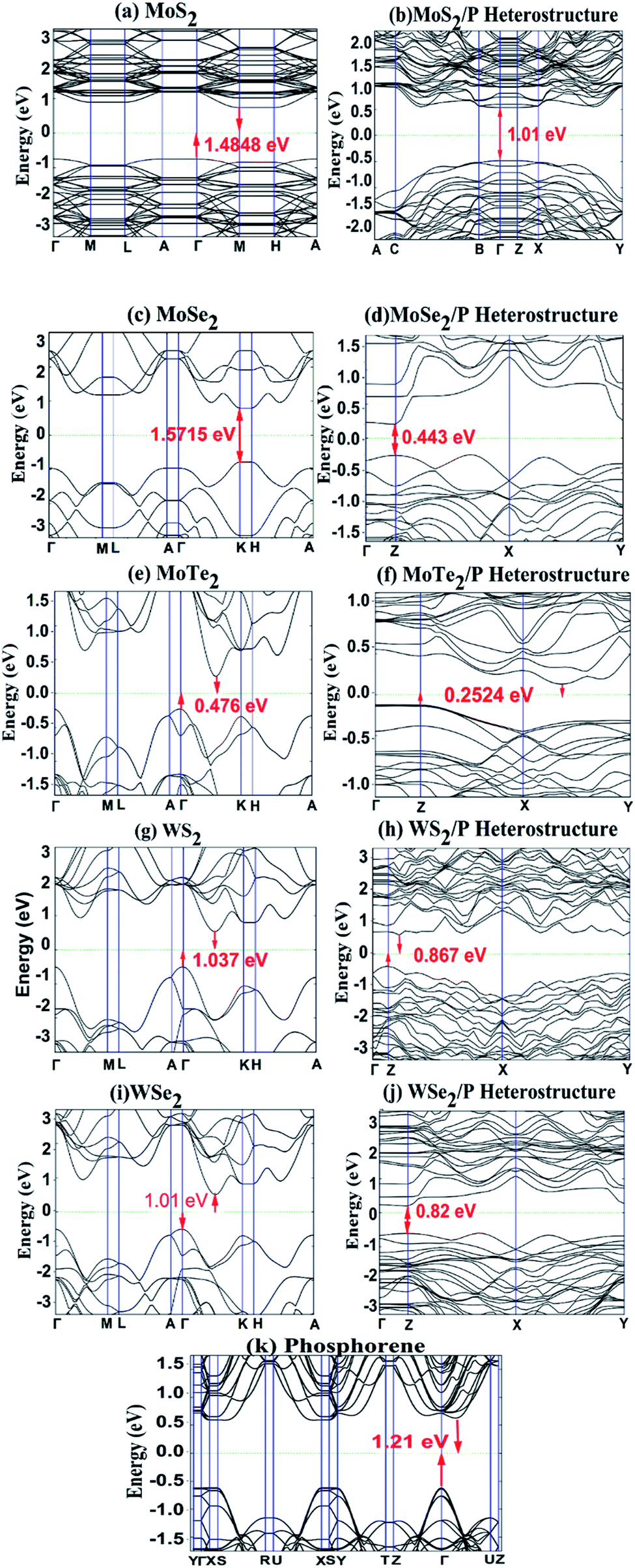 | ||
| Fig. 6 Band structure of (a) MoS2, (c) MoSe2, (e) MoTe2 (g) WS2, (i) WSe2 and (k) phosphorene, and heterostructures of (b) MoS2/P, (d) MoSe2/P, (f) MoTe2/P, (h) WS2/P and (j) WSe2/P, with their bandgaps. | ||
D. Band alignment
It is important know the type of band alignment in a material for its use in optical and solar cell applications. Band alignment is computed in Fig. 7 using the valence band and conduction band offsets from their heterostructure interface calculations.68 | ||
| Fig. 7 Band alignment of resultant TMD/phosphorene heterostructures. | ||
From Fig. 7, it can be observed that all the heterostructures are having type-II band alignments except WSe2/P heterostructure. This type of band alignment is important as it helps to separate electron and holes in a natural way, which makes the heterostructures excellent for application in optoelectronics and solar energy conversion.61
Further moving away from heterostructure interface to the region where only monolayer of MoS2/MoSe2/MoTe2/WS2/WSe2 is present, a small band bending is observed in all the structures. The difference between the heterostructure's potential (work function (W) and the monolayer's potential (Ws) gives the value of this band bending: ΔEf = W − Ws. The band bending values for MoS2, MoSe2, MoTe2, WS2 and WSe2 obtained are 0.16, 0.18, 0.56, 0.13 and 0.12, respectively, and for phosphorene it is −0.998. This suggests that electrons transition will be taken place from MoS2/MoSe2/MoTe2/WS2/WSe2 to phosphorene. This happens because when two layers with distinct work functions are stacked, then there exists charge transfer from both sides to neutralize the work function differences between the two layers.
IV. Conclusions
In summary, first principle calculations are performed to study the stacking effect on optoelectronic properties of the heterostructures of MoS2/P, MoSe2/P, MoTe2/P, WS2/P, and WSe2/P. The results suggest a wide usable spectrum in the visible region with high absorption coefficient values in this region in the heterostructures. Higher visible region absorption is seen in the heterostructures as compared to the monolayers. Also, these results are in confirmation with the trends in dielectric constants and refractive index. The results suggest a large improvement in desired visible region absorption, thereby, increasing the usefulness of TMD based phosphorene heterostructures in solar energy conversion applications and optoelectronic devices.Conflicts of interest
There are no conflicts to declare.References
- A. K. Geim and K. S. Novoselov, The rise of graphene, Nat. Mater., 2007, 6, 183–191 CrossRef CAS PubMed.
- C. Berger, et al., Ultrathin epitaxial graphite “2D electron gas properties and a route toward graphene-based nanoelectronics”, J. Phys. Chem. B, 2004, 108, 19912–19916 CrossRef CAS.
- S. Stankovich, et al., Graphene-based composite materials, Nature, 2006, 442, 282–286 CrossRef CAS PubMed.
- C. Berger, et al., Ultrathin epitaxial graphite: 2D electron gas properties and a route toward graphene-based nanoelectronics, J. Phys. Chem. B, 2004, 108, 19912–19916 CrossRef CAS.
- M. J. Allen, V. C. Tung and R. B. Kaner, Honeycomb carbon: a review of graphene, Chem. Rev., 2010, 110(1), 132–145 CrossRef CAS PubMed.
- A. H. C. Neto, F. Guinea, N. M. R. Peres, K. S. Novoselov and A. K. Geim, The electronic properties of graphene, Rev. Mod. Phys., 2009, 81(1), 109–162 CrossRef.
- Z. Ni, et al., Tunable bandgap in silicene and germanene, Nano Lett., 2012, 12(1), 113–118 CrossRef CAS PubMed.
- P. Vogt, et al., Silicene: compelling experimental evidence for graphene-like two-dimensional silicon, Phys. Rev. Lett., 2012, 108(15), 155501 CrossRef PubMed.
- H. Liu, et al., Phosphorene: an unexplored 2D semiconductor with high hole mobility, ACS Nano, 2014, 8(4), 4033–4041 CrossRef CAS PubMed.
- X. Duan, C. Wang, A. Pan, R. Yu and X. Duan, Two-dimensional transition metal dichalcogenides as atomically thin semiconductors: opportunities and challenge, Chem. Soc. Rev., 2015, 44(24), 8859–8876 RSC.
- J. Wang, F. Ma and M. Sun, Graphene, hexagonal boron nitride, and their heterostructures: properties and applications, RSC Adv., 2017, 7, 16801–16822 RSC.
- F. Zhang, W. Li, Y. Ma, Y. Tang and X. Dai, Tuning the Schottky contacts at the graphene/WS2 interface by electric field, RSC Adv., 2017, 7, 29350–29356 RSC.
- N. R. Pradhan, et al., Metal to insulator quantum-phase transition in few-layered ReS2, Nano Lett., 2015, 15(12), 8377–8384 CrossRef CAS PubMed.
- B. Liu, M. Cai, Y. Zhao, L. Wu and L. Wang, First-principles Investigation of the Schottky Contact for the Two-Dimensional MoS2 and Graphene Heterostructure, RSC Adv., 2016, 6, 60271–60276 RSC.
- A. Eftekhari, Tungsten dichalcogenides (WS2, WSe2, and WTe2): material chemistry and applications, J. Mater. Chem. A, 2017, 5(35), 18299–18325 RSC.
- U. Wurstbauer, B. Miller, E. Parzinger and A. W. Holleitner, Light–matter interaction in transition metal dichalcogenides and their heterostructures, J. Phys. D: Appl. Phys., 2017, 50(17), 173001 CrossRef.
- K. F. Mak, et al., Atomically thin MoS2: a new direct-gap semiconductor, Phys. Rev. Lett., 2010, 105, 136805 CrossRef PubMed.
- L. F. Mattheis, Band structures of transition-metal-dichalcogenide layer compounds, Phys. Rev. B: Condens. Matter Mater. Phys., 1973, 8(8), 3719 CrossRef.
- R. A. Bromley, R. B. Murray and A. D. Yoffe, The band structures of some transition metal dichalcogenides. III. Group VIA: trigonal prism materials, J. Phys. C: Solid State Phys., 1972, 5(7), 759–778 CrossRef CAS.
- T. Böker, et al., Band structure of MoS2, MoSe2, and α-MoTe2: angle resolved photoelectron spectroscopy and ab initio calculations, Phys. Rev. B: Condens. Matter Mater. Phys., 2001, 64(23), 235305 CrossRef.
- K. S. Novoselov, Two-dimensional atomic crystals, Proc. Natl. Acad. Sci. U. S. A., 2005, 102(30), 10451–10453 CrossRef CAS PubMed.
- K. F. Mak, K. He, J. Shan and T. F. Heinz, Control of valley polarization in monolayer MoS2 by optical helicity, Nat. Nanotechnol., 2012, 7, 494–498 CrossRef CAS PubMed.
- O. Lopez-Sanchez, D. Lembke, M. Kayci, A. Radenovic and A. Kis, Ultrasensitive photodetectors based on monolayer MoS2, Nat. Nanotechnol., 2013, 8, 497–501 CrossRef CAS PubMed.
- W. Choi, et al., High-detectivity multilayer MoS2 phototransistors with spectral response from ultraviolet to infrared, Adv. Mater., 2012, 24(43), 5832–5836 CrossRef CAS PubMed.
- K. He, C. Poole, K. F. Mak and J. Shan, Experimental demonstration of continuous electronic structure tuning via strain in atomically thin MoS2, Nano Lett., 2013, 13(6), 2931–2936 CrossRef CAS PubMed.
- J. Wang, H. Shu, P. Liang, N. Wang, D. Cao and X. Chen, Thickness-Dependent Phase Stability and Electronic Properties of GaN Nanosheets and MoS2/GaN van der Waals Heterostructures, J. Phys. Chem. C, 2019, 123(6), 3861–3867 CrossRef CAS.
- P. A. Nwofe, K. T. Ramakrishna Reddy, J. K. Tan, I. Forbes and R. W. Miles, Thickness Dependent Optical Properties of Thermally Evaporated SnS Thin Films, Phys. Procedia, 2012, 25, 150–157 CrossRef CAS.
- R. A. B. Villaos, C. P. Crisostomo, Z.-Q. Huang, S.-M. Huang, A. A. B. Padama, M. A. Albao, H. Lin and F.-C. Chuang, Thickness dependent electronic properties of Pt dichalcogenides, npj 2D Mater. Appl., 2019, 3, 2 CrossRef.
- P. Tyagi, A. G. Vedeshwar and N. C. Mehra, Thickness dependent optical properties of CdI2 films, Phys. B, 2001, 304(Issues 1–4), 166–174 CrossRef CAS.
- A. Zubair, M. T. Choudhary, M. S. Bashar and M. A. Sami, Thickness dependent correlation between structural and optical properties of textured CdSe thin film, AIP Adv., 2019, 9, 045123 CrossRef.
- H. I. Ifkere, A. Tatarogulu and S. S. Cetin, et al., The effect of thickness on the optical, structural and electrical properties of ZnO thin film deposited on n-type Si, J. Mol. Struct., 2018, 1165, 376–380 CrossRef.
- A. S. Solieman, M. M. Hafiz, A.-hamid A. Abu-Sehly and A.-naser A. Alfaqeer, Dependence of optical properties on the thickness of amorphous Ge30Se70 thin films, Journal of Taibah University for Science, 2014, 8(3), 282–288 CrossRef.
- B. Radisavljevic, A. Radenovic, J. Brivio, V. Giacometti and A. Kis, Single-layer MoS2 transistors, Nat. Nanotechnol., 2011, 6, 147–150 CrossRef CAS PubMed.
- Y. Deng, et al., Black phosphorus-monolayer MoS2 van der Waals heterojunction p–n diode, ACS Nano, 2014, 8292–8299 CrossRef CAS PubMed.
- H. Zhang, Y. N. Zhang, H. Liu and L. M. Liu, Novel heterostructures by stacking layered molybdenum disulfides and nitrides for solar energy conversion, J. Mater. Chem. A, 2014, 15389–15395 RSC.
- J. Liao, B. Sa, J. Zhou, R. Ahuja and Z. Sun, Design of high-efficiency visible-light photocatalysts for water splitting: MoS2/AlN (GaN) heterostructure, J. Phys. Chem. C, 2014, 118, 17594–17599 CrossRef CAS.
- S. Choudhary and A. K. Garg, Enhanced absorption in MoS2/Hg0.33Cd0.66Te Heterostructure for application in solar cell absorbers, IEEE Trans. Nanotechnol., 2019, 18, 989–994 CAS.
- H. Liu, et al., Phosphorene: an unexplored 2D semiconductor with high hole mobility, ACS Nano, 2014, 8(4), 4033–4041 CrossRef CAS PubMed.
- S. Kaur, A. Kumar, S. Srivastava and K. Tankeshwar, van der Waals heterostructures based on allotropes of phosphorene and MoSe2, Phys. Chem. Chem. Phys., 2017, 19(33), 22023–22032 RSC.
- L. Li, et al., Black phosphorus field-effect transistors, Nat. Nanotechnol., 2014, 9, 372–377 CrossRef CAS PubMed.
- E. S. Reich, Phosphorene excites materials scientists, Nature, 2014, 506, 19 CrossRef PubMed.
- R. Kochar and S. Choudhary, MoS2/phosphorene heterostructure for optical absorption in the visible region, IEEE J. Quantum Electron., 2018, 54(4), 7000306 Search PubMed.
- Y. Takao and A. Morita, Electronic structure of black phosphorus: tight binding approach, Physica B+C, 1981, 105(1–3), 93–98 CrossRef CAS.
- J. Qiao, X. Kong, Z.-X. Hu, F. Yang and W. Ji, High-mobility transport anisotropy and linear dichroism in few-layer black phosphorus, Nat. Commun., 2014, 5, 4475 CrossRef CAS PubMed.
- L. Liang, J. Wang, W. Lin, B. G. Sumpter, V. Meunier and M. Pan, Electronic bandgap and edge reconstruction in phosphorene materials, Nano Lett., 2014, 14(11), 6400–6406 CrossRef CAS PubMed.
- L. Kou, T. Frauenheim and C. Chen, Phosphorene as a superior gas sensor: selective adsorption and distinct I–V response, J. Phys. Chem. Lett., 2014, 5(15), 2675–2681 CrossRef CAS PubMed.
- L. Wang, A. Kutana, X. Zou and B. I. Yakobson, Electro-mechanical anisotropy of phosphorene, Nanoscale, 2015, 7(21), 9746–9751 RSC.
- J.-W. Jiang and H. S. Park, Mechanical properties of single-layer black phosphorus, J. Phys. D: Appl. Phys., 2014, 47(38), 385304 CrossRef.
- Z. Sun, A. Martinez and F. Wang, Optical modulators with 2D layered materials, Nat. Photonics, 2016, 10(4), 227–238 CrossRef CAS.
- T. Roy, et al., Dual-gated MoS2/WSe2 van der Waals tunnel diodes and transistors, ACS Nano, 2015, 9(2), 2071–2079 CrossRef CAS PubMed.
- M.-H. Chiu, et al., Determination of band alignment in the single-layer MoS2/WSe2 heterojunction, Nat. Commun., 2015, 6, 7666 CrossRef CAS PubMed.
- R. Cheng, et al., Electroluminescence and photocurrent generation from atomically sharp WSe2/MoS2 heterojunction p–n diodes, Nano Lett., 2014, 14(10), 5590–5597 CrossRef CAS PubMed.
- P. Rivero, C. M. Horvath, Z. Zhu, J. Guan, D. Tománek and S. Barraza-Lopez, Simulated scanning tunneling microscopy images of few-layer phosphorus capped by graphene and hexagonal boron nitride monolayers, Phys. Rev. B: Condens. Matter Mater. Phys., 2015, 91(11), 115413 CrossRef.
- F. Yi, H. Ren, J. Shan, X. Sun, D. Wei and Z. Liu, Wearable energy sources based on 2D materials, Chem. Soc. Rev., 2018, 47(9), 3152–3188 RSC.
- C. Chen, et al., MoS2-on-MXene heterostructures as highly reversible anode materials for lithium-ion batteries, Angew. Chem., 2018, 130(7), 1864–1868 CrossRef.
- Q. Peng, et al., Electronic structures and enhanced optical properties of blue phosphorene/transition metal dichalcogenides van der Waals heterostructures, Sci. Rep., 2016, 6, 31994 CrossRef CAS PubMed.
- M. Naguib, et al., New two-dimensional niobium and vanadium carbides as promising materials for Li-ion batteries, J. Am. Chem. Soc., 2013, 135(43), 15966–15969 CrossRef CAS PubMed.
- O. Mashtalir, et al., Intercalation and delamination of layered carbides and carbonitrides, Nat. Commun., 2013, 4, 1716 CrossRef PubMed.
- J. P. Perdew, K. Burke and M. Ernzerhof, Generalized gradient approximation made simple, Phys. Rev. Lett., 1996, 77(18), 3865 CrossRef CAS PubMed.
- G. Kresse and J. Furthmüller, Efficient iterative schemes for ab initio total-energy calculations using a plane-wave basis set, Phys. Rev. B: Condens. Matter Mater. Phys., 1996, 54, 11169 CrossRef CAS PubMed.
- S. Grimme, Semiempirical GGA-type density functional constructed with a long-range dispersion correction, J. Comput. Chem., 2006, 27(15), 1787–1799 CrossRef CAS PubMed.
- F. Tran and P. Blaha, Accurate band gaps of semiconductors and insulators with a semilocal exchange-correlation potential, Phys. Rev. Lett., 2009, 102(22), 226401 CrossRef PubMed.
- R. M. Martin, Electronic Structure: Basic Theory and Practical Methods, New York, NY, USA, Cambridge Univ. Press, 2014 Search PubMed.
- D. J. Griffithis, Introduction to Electrodynamics, Upper Saddle River, NJ, USA, Prentice-Hall, 1999 Search PubMed.
- M.-Y. Li, C.-H. Chen, Y. Shi and L.-J. Li, Heterostructures based on two-dimensional layered materials and their potential applications, Mater. Today, 2015, 19(6), 322–335 CrossRef.
- L.-J. Kong, G.-H. Liu and Y.-J. Zhang, Tuning the electronic and optical properties of phosphorene by transition-metal and nonmetallic atom co-doping, RSC Adv., 2016, 6(13), 10919–10929 RSC.
- M. Zhao, et al., Interlayer coupling in anisotropic/isotropic van der Waals heterostructures of ReS2 and MoS monolayers, Nano Res., 2016, 9, 3772–3780 CrossRef CAS.
- Y. Hinuma, A. Grüneis, G. Kresse and F. Oba, Band alignment of semiconductors from density-functional theory and many-body perturbation theory, Phys. Rev. B: Condens. Matter Mater. Phys., 2014, 90, 155405 CrossRef.
| This journal is © The Royal Society of Chemistry 2020 |