
 Open Access Article
 This Open Access Article is licensed under a Creative Commons Attribution-Non Commercial 3.0 Unported Licence
Improving the internal quantum efficiency of QD/QW hybrid structures by increasing the GaN barrier thickness
Zhigang Jia *a,
Xiaodong Haob,
Taiping Lua,
Hailiang Donga,
Zhiwei Jiac,
Shufang Mab,
Jian Lianga,
Wei Jiaa and
Bingshe Xuab
*a,
Xiaodong Haob,
Taiping Lua,
Hailiang Donga,
Zhiwei Jiac,
Shufang Mab,
Jian Lianga,
Wei Jiaa and
Bingshe Xuab
aKey Laboratory of Interface Science and Engineering in Advanced Materials, Taiyuan University of Technology, Ministry of Education, Taiyuan 030024, China. E-mail: jiazhigang@tyut.edu.cn
bInstitute of Atomic and Molecular Science, Shanxi University of Science and Technology, Xi'an 710021, China
cKey Laboratory of Advanced Transducers and Intelligent Control System, Taiyuan University of Technology, Ministry of Education, Taiyuan 030024, China
First published on 12th November 2020
Abstract
Three InGaN/GaN quantum well (QW) samples with different barrier thickness (Sample A: 15 nm, Sample B: 17.5 nm, and Sample C: 20 nm) were grown via a metal organic chemical vapor deposition (MOCVD) system. The InGaN/GaN QWs became QD/QW hybrid structures due to the high density of V-shaped pits (VPs), which cut the InGaN wells into InGaN quantum dots (QDs) and indium-rich (In-rich) QDs stemming from the indium phase separation. By increasing the thickness of GaN barriers, the interactions between InGaN wells are weakened; thus, the strain accumulation is relieved and the strain relaxation degree decreases. Abnormally, the residual internal strain first increased due to least VPs in B and then decreased for C. Lower internal strain weakens the strain-induced piezoelectric polarization effect and as a result, a higher electron–hole wave function overlap and radiative recombination efficiency are improved. Similarly, lower strain relaxation results in more homogeneous indium distribution, and accordingly, a slightly weaker carrier localization effect (CLE). The CLEs of the three samples are strong enough that carriers can be confined by localized states even at room temperature; thus, the slightly weaker CLE does not influence the internal quantum efficiency (IQE). More importantly, InGaN QDs or QWs with lower strain relaxation contain fewer stacking faults that can act as non-radiative recombination centers (NRRCs), improving the IQE. By analyzing the effects of strain-induced piezoelectric polarization, NRRCs and carrier localization on the IQE, it is found that less NRRCs are a major factor in improving the IQE of these QD/QW hybrid structures.
Introduction
InGaN/GaN quantum wells (QWs) have been widely applied as the active region of light emitting diodes (LEDs) and laser diodes (LDs) in the blue, green and even yellow spectral regions.1–3 However, the internal quantum efficiency (IQE) of InGaN/GaN QWs drop dramatically when the emission wavelength shifts from the blue to green region. This problem is well known as the “green gap”,4–6 which is mainly caused by the high defect density and the quantum confined Stark effect (QCSE).7,8 Fortunately, indium-rich (i.e., In-rich) quantum dots (QDs) offer researchers a promising approach to realize higher IQEs. In-rich QDs were discovered by Shuji Nakamura when he investigated the recombination mechanism of InGaN LED and LD,9,10 and the carrier localization effect arising from the formation of In-rich QDs was proved to be the main mechanism of radiative recombination.11–13 Generally, by adjusting the growth parameters of InGaN/GaN QWs or altering their structures appropriately, the number of In-rich QDs will be measurably increased, and accordingly, a layer of QDs form at the interface between InGaN and GaN due to the phase separation process of the InGaN layer14 and Stranski–Krastanow (S–K) mode.15 Compared with InGaN quantum wells (QWs), InGaN QDs have lower piezoelectric polarization fields16,17 and stronger carrier localization effects.18 These two advantages contribute to the enhancement of IQE. In our previous work, with the increment of the InGaN layer thickness, the two-dimensional step flow surface morphology was transformed to an island-shaped morphology, and the IQE increased significantly due to the enhancement of the carrier localization effect and reduced non-radiative recombination centers (NRRCs).19 The enhanced carrier localization effect can be attributed to the formation of In-rich QDs. Because of the formation of In-rich QDs, InGaN/GaN QWs may become a kind of QD/QW hybrid structure.Increasing the thickness of the InGaN wells induces a stronger carrier localization effect and higher IQE; however, at the same time, stronger strain accumulation is an inevitable disadvantage for the InGaN/GaN QWs. Strain accumulation has already been investigated in InGaN/GaN QWs20,21 and stacked InAs-GaAs QDs.22 The relaxation of the accumulated stain deteriorates the interfacial structure and crystal quality.23 Moreover, strain-compensated layers and thicker barriers were employed to reduce the strain accumulation.24,25 Similarly, strain can be stored in our hybrid structures and cause degradation of the crystal quality; thicker GaN barriers or strain-compensated layers could be promising solutions.
In this work, six-period InGaN/GaN QWs grown with different GaN barrier thicknesses of 15 nm (Sample A), 17.5 nm (Sample B), and 20 nm (Sample C) were transformed into QD/QW hybrid structures due to their high densities of V-shaped pits (VPs). The surface morphologies and cross-section views were observed by AFM and TEM. The variations of the piezoelectric polarization field and carrier localization effect were analysed by excitation power density dependent photoluminescence (EPDD-PL) and temperature-dependent photoluminescence (TD-PL) measurements. It was found that the density of the NRRCs decreases at a thicker GaN barrier, and accordingly, IQE increases.
Experimental details
All samples were grown on c-plane (0001) sapphire substrates via an Aixtron TS300 metal organic chemical vapor deposition (MOCVD) system. Trimethylgallium (TMGa), triethylgallium (TEGa), trimethylindium (TMIn) and ammonia (NH3) were used as precursors. All the metal–organic sources were purchased from Nata OPTO-ELECTRONIC MATERIAL Co., Ltd, and NH3 was purchased from Guangdong Huate Gas Co., Ltd. The purity of all metal–organic sources and NH3 is higher than 99.9999%. First, the substrate was exposed to H2 at 1120 °C for six minutes to remove impurities. Then, a 25 nm-thick GaN nucleation layer was grown at 530 °C. After annealing at 1070 °C, a 3 μm nominal undoped GaN (U-GaN) layer was deposited. The nucleation layer and U-GaN were prepared using TMGa as the Ga source. Finally, the carrier gas was changed from H2 to N2, and TEGa was used as a gallium source to grow six-period InGaN/GaN periodic structures. The InGaN layers and GaN barriers were grown at 715 °C and 850 °C, respectively. In order to prevent indium from desorbing from the InGaN layer surface during the temperature ramping process, a 1 nm-thick GaN capping layer was deposited immediately after the growth of each InGaN layer without changing the growth temperature. Three samples, denoted as A, B and C, were grown with different nominal barrier thicknesses (A: 15 nm, B: 17.5 nm and C: 20 nm) while the other growth parameters were kept constant. The mole flow of TEGa determines the growth rate of the GaN barriers. In the growth procedure of InGaN/GaN QWs, the mole flow of TEGa remains constant, generating a constant growth rate of the GaN barriers. Different barrier thicknesses were obtained by varying the growth time of the GaN barriers (A: 300 s, B: 350 s, C: 400 s). The nominal thickness of the InGaN layers estimated through XRD is about 4 nm, as the growth times of the InGaN wells were all 120 s, leading to the same thicknesses. However, because of the high density of V-shaped pits, strain relaxation and indium segregation, the thickness of the InGaN layers is not uniform as seen in perfect quantum wells but ranges from 3 nm to 7 nm according to the TEM measurements.Tapping-mode atomic force microscopy (AFM) was used to characterize the surface morphologies of the three samples. The cross-section views (including TEM, HAADF, EDS, and HRTEM images) were observed by a Talos F200X scanning transmission electron microscope (STEM) at an accelerating voltage of 200 kV. The piezoelectric polarization effect and carrier localization effect (CLE) were studied by EPDD-PL and TD-PL measurements, respectively. The EPDD-PL spectra were obtained using a 266 nm continuous wave laser at room temperature, and the excitation power density varied in the range of 1.35–42.3 W cm−2. The TD-PL spectra were measured from 10 to 300 K with a 325 nm He–Cd continuous wave laser, and the excitation power density was 2.65 W cm−2.
Results and discussion
The three samples are labeled as Sample A, Sample B and Sample C. Their nominal barrier thicknesses are 15 nm (Sample A), 17.5 nm (Sample B) and 20 nm (Sample C). In this section, the surface morphologies, especially the V-shaped pits (VPs), were firstly characterized and researched by AFM and TEM; then, the piezoelectric polarization effects and carrier localization effects (CLE) of the samples were analyzed through EPDD-PL and TD-PL measurements, respectively; and finally, the non-radiative recombination centers (NRRCs) were observed and analyzed via HRTEM.1. V-shaped pits on the surface and QD/QW structures
Fig. 1 (a), (b) and (c) show the three-dimensional (3D) AFM images of Samples A, B and C, respectively. It can be observed that Samples A and C have clear and distinct 3D island-shaped morphologies. Unlike S–K mode or V–W mode QDs, the 3D island-shaped morphology appears to form due to high-density pits occurring on the surface. Sample B contains both a 3D island-shaped morphology and two-dimensional step-flow morphology.26,27 Similarly, a large number of pits occur on the surface; however, the density of the pits is lower than those of Samples A and C. Fig. 1(d) shows cross-section profiles of Samples A, B and C. These profiles are cut out from the middle of Fig. 1 (a), (b) and (c), respectively. Profiles A, B and C span 32, 18 and 37 pits, and their average depths are 6.3 nm, 4.6 nm and 12.7 nm, respectively. Correspondingly, the RMS roughnesses of A, B and C are 3.68 nm, 2.45 nm and 7.79 nm. Obviously, Sample B has the shallowest pits; C has the deepest pits; and A is in between. The trend of inconsistent variations of the barriers' thicknesses will be discussed after the TEM and HAADF analysis. All the pits may be VPs; however, this cannot be asserted only through AFM measurements. In order to prove this assumption, TEM images, HAADF images and EDS mappings of Sample A, B and C are shown in Fig. 2 and 3.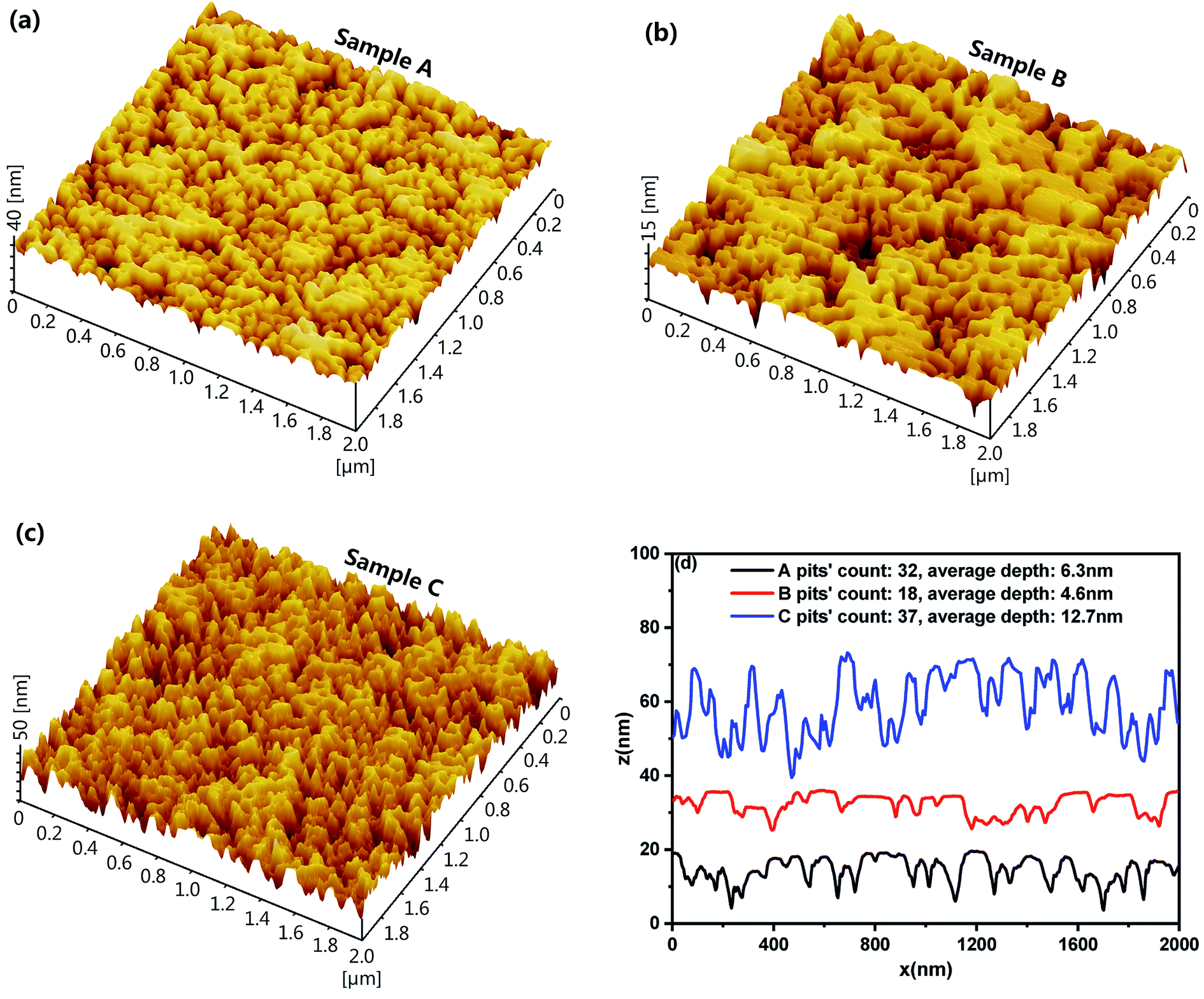 | ||
| Fig. 1 3D AFM images (2 × 2 μm) of (a) Sample A, (b) Sample B, and (c) Sample C and (d) their cross-section profiles. | ||
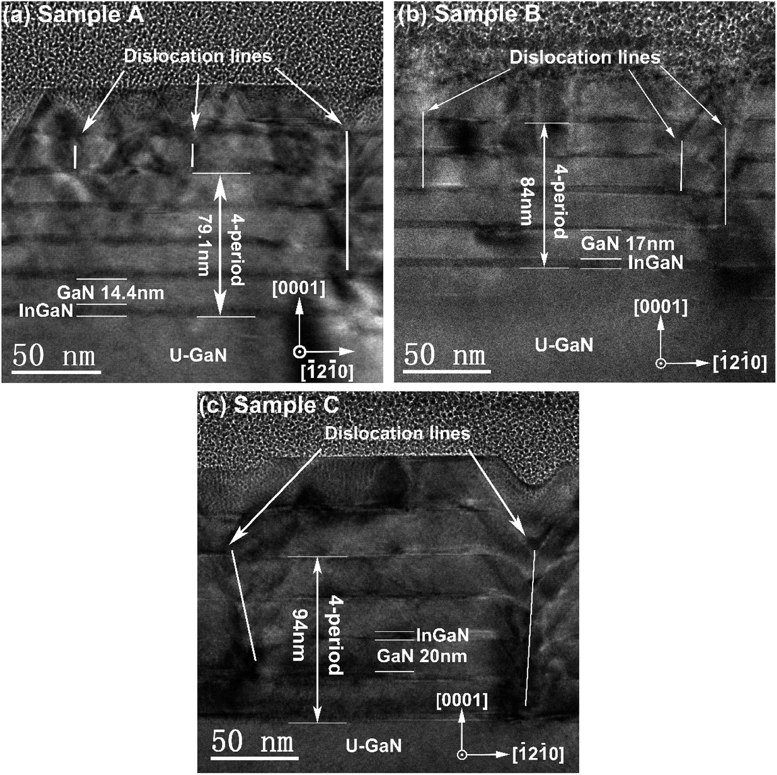 | ||
| Fig. 2 TEM images of (a) Sample A, (b) Sample B and (c) Sample C. | ||
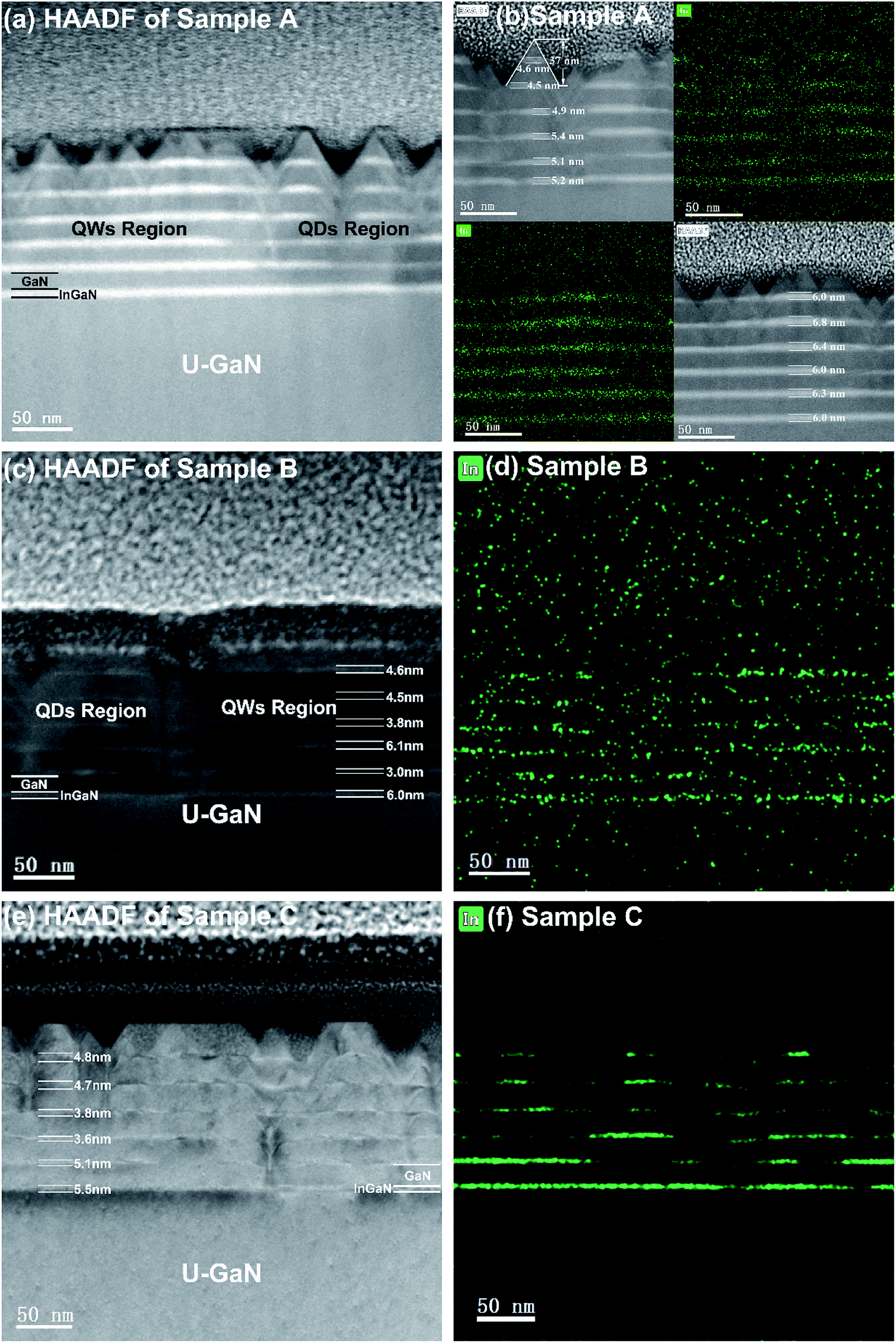 | ||
| Fig. 3 HAADF images of (a) Sample A, (c) Sample B and (e) Sample C; (b) HAADF images and EDS mappings of the QDs region and QWs region in Sample A; EDS mappings of (d) B and (f) C. | ||
In Fig. 2, it can be seen that all the pits on the surface are VPs, because these pits have {10![[1 with combining macron]](https://www.rsc.org/images/entities/char_0031_0304.gif) 1} side walls which are at a 62° angle to the c-plane. This is consistent with previous reports.28,29 In Fig. 2(a), it can be seen that Sample A contains several small VPs which start from the fifth or the top (the sixth) InGaN QW, one medium-sized VP located at the left edge of Fig. 2(a), and one large VP originating from the second InGaN QW. In Fig. 2(b), there is one large VP starting from the second QW, two medium-sized VPs starting from the third InGaN QW, and two small VPs forming at the fourth or the fifth InGaN QW. In Fig. 2(c), two large VPs form at the bottom and the second InGaN QW. On the other hand, Sample B has the sharpest and the smoothest InGaN/GaN interfaces, and A has the blurriest InGaN/GaN interfaces. It is surprising that sample C does not have the smoothest interfaces. This abnormal result can be explained by combining the AFM, TEM and HAADF results. In addition, the layer thicknesses were measured through TEM. It was found that the average periodic thickness of sample A (19.8 nm) was higher than the expected 19 nm, while the average periodic thicknesses of sample B (21 nm) and C (23.5 nm) were lower than the expected 21.5 nm and 24 nm. The average thicknesses of the InGaN layers are higher than expected (4 nm) because of the high density of V-shaped pits, strain relaxation and indium segregation. The thicknesses of the InGaN layers will be given in the HAADF analysis.
1} side walls which are at a 62° angle to the c-plane. This is consistent with previous reports.28,29 In Fig. 2(a), it can be seen that Sample A contains several small VPs which start from the fifth or the top (the sixth) InGaN QW, one medium-sized VP located at the left edge of Fig. 2(a), and one large VP originating from the second InGaN QW. In Fig. 2(b), there is one large VP starting from the second QW, two medium-sized VPs starting from the third InGaN QW, and two small VPs forming at the fourth or the fifth InGaN QW. In Fig. 2(c), two large VPs form at the bottom and the second InGaN QW. On the other hand, Sample B has the sharpest and the smoothest InGaN/GaN interfaces, and A has the blurriest InGaN/GaN interfaces. It is surprising that sample C does not have the smoothest interfaces. This abnormal result can be explained by combining the AFM, TEM and HAADF results. In addition, the layer thicknesses were measured through TEM. It was found that the average periodic thickness of sample A (19.8 nm) was higher than the expected 19 nm, while the average periodic thicknesses of sample B (21 nm) and C (23.5 nm) were lower than the expected 21.5 nm and 24 nm. The average thicknesses of the InGaN layers are higher than expected (4 nm) because of the high density of V-shaped pits, strain relaxation and indium segregation. The thicknesses of the InGaN layers will be given in the HAADF analysis.
Fig. 3(a) shows the HAADF image of a typical cross section of Sample A. Seven small VPs and three large VPs are visible. In the large VPs, InGaN wells grow on the {101} side walls, and the indium fraction is much lower than that in the InGaN wells grown on the c-plane. As a result, the c-plane InGaN wells are cut into vertically aligned InGaN QDs by the adjacent large VPs, and the mobility pathways of indium atom are simultaneously cut off, as shown in the right part of Fig. 3(a). This region is labelled as the QDs region. Likewise, EDS mapping of the region demonstrates two columns of QDs (Fig. 3(b)). On the left of the vertically aligned InGaN QDs are continuous InGaN wells under the small VPs. This region is labelled as the QWs region. The adjacent QDs and QWs regions constitute the QD/QW hybrid structure. In the entire QD/QW hybrid structure, clear indium segregation exists, inducing a large amount of In-rich QDs. Fig. 3(c) shows the HAADF image of Sample B. Only three large VPs and one small VP can be observed. The three large VPs cut the InGaN QWs into vertically aligned InGaN QDs. This region can be thought of as InGaN QDs. However, the InGaN layers in the QWs region are also slightly cut off according to the EDS mapping (Fig. 3(d)), increasing the number of cut QDs. Indium segregation and In-rich QDs can also be observed in the HAADF image, although sample B has the smoothest InGaN/GaN interfaces. Fig. 3(e) shows an HAADF image of Sample C; five relatively large VPs and three small VPs can be seen, and the corresponding EDS mapping shown in Fig. 3(f) demonstrates that some of the InGaN wells are cut into QDs. The QDs and QWs regions cannot be clearly distinguished. QDs are mixed with QWs to form another type of QD/QW hybrid structure. The thickness of the InGaN layers of the three samples ranges from 3 nm to 7 nm. Most of the InGaN layers are thicker than expected (4 nm). The obvious thickness variation of the InGaN layers can be attributed to VPs, strain relaxation and indium segregation. Increasing the InGaN layer thickness led to decreased thickness of the GaN barriers.
Through analyzing these AFM, TEM, and HAADF images and EDS mappings, it can be concluded that the InGaN/GaN QWs become QD/QW hybrid structures due to the formation of a high density of VPs. Sample B has the fewest and the shallowest VPs. A and B contain more small VPs; however, Sample C contains more large VPs. The trend is consistent with the AFM results. A has the highest accumulated strain, which induces the formation of a large number of medium and small V-shaped pits generated at the third to sixth InGaN wells. Simultaneously, large VPs form at the bottom or second InGaN wells due to threading dislocations occurring in U-GaN. Relative to A, B has a thicker GaN barrier, relieving the accumulated strain to some degree. As a result, fewer and shallower V-shaped pits are generated on the surface of B. Differently, the thickest GaN barrier of C almost isolates the interaction between the InGaN wells, further reducing the accumulated strain; thus, few small V-shaped pits are generated on the surface of C, and only the large V-shaped pits forming at the threading dislocations can penetrate the wells and barriers. More large VPs cut off the mobility path of indium atoms, resulting in a relatively rough InGaN/GaN interface compared to Sample B. Meanwhile, the large VPs in Sample C cut the InGaN wells into more QDs, which can relax strain more effectively than QWs due to their nanoscale size. Given this, the internal strain of C may be the lowest; however, the formation of VPs is not the only pathway of strain relaxation, and the strain accumulation also influences the internal strain.
2. Reduced internal strain and piezoelectric polarization effects
The thickest barrier of C could isolate the interaction between the InGaN wells, reducing strain accumulation. Conversely, strain accumulates to the largest degree in A due to the thinnest barriers. The strain relaxation degree was estimated by (115) reciprocal space mapping scanned by a Bruker D8 Advance HRXRD. Sample C has the lowest relaxation degree of 4.1%, and A has the highest relaxation degree of 8.2%. The relaxation degree of B (7.5%) is in between and is closer to that of A than of C. This trend is consistent with the thickness variation of the GaN barriers because the layer thicknesses of B are more similar to those of A than of C, as shown in Fig. 2. Currently, the variation of the internal strain cannot be determined; however, the internal strain of the InGaN layers determines the strain-induced piezoelectric polarization effects, which can be analyzed by EPDD-PL measurements, as shown in Fig. 4. Therefore, the internal strain variation trend can be characterized by EPDD-PL.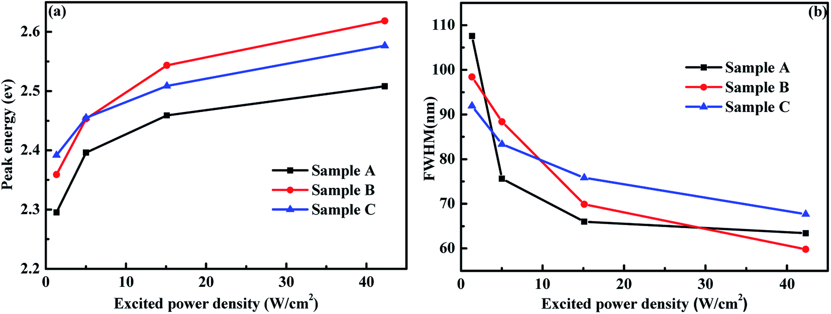 | ||
| Fig. 4 The excitation power density dependence of the (a) peak energy and (b) FWHM. | ||
For all three samples, the peak energy increases (blue-shift) when the excitation power density rises, which may stem from the screening effect of the polarization field or the band filling effect.11,32 Simultaneously, the full width at half maximum (FWHM) reduces. A higher excitation power density can excite a larger population of photogenerated carriers to screen the polarization field, resulting in an increase of the peak energy (blue-shift of emission wavelength).11,30–32 Also, the blue-shift could stem from the band filling effect.11,32 The narrowed FWHM may be related to the screening effect of the polarization field;32 however, a band filling effect would result in a broadened FWHM.32 According to the results in Fig. 4(b), the band filling effect does not occur. The screening effect of the polarization field should be the main reason for the blue-shift. The blue-shift of C (180 meV) is the smallest, and the blue-shift of sample B (260 meV) is the largest, slightly larger than that of sample A (210 meV). These results indicate that the order of the polarization fields should be B > A > C. The results indicate that B has the highest residual internal strain rather than being in-between. This abnormal trend will be explained in the last section. As the internal strain decreases, the piezoelectric polarization field is reduced and the wave functions of electrons and holes achieve more overlap, inducing a higher radiative recombination possibility and IQE. On the other hand, CLE can inhibit the non-radiative recombination process to improve the radiative recombination possibility and IQE. However, defects generated during the strain relaxation process may capture carriers and lead to non-radiative recombination. In the next two sections, the effects of the CLE and defects will be respectively discussed.
3. Carrier localization effects
The CLE is an important feature of these QD/QW structures, and it was investigated using TD-PL measurements (Fig. 5). As shown in Fig. 5, the peak energy monotonically increases with growing temperature, unlike the typical “S-shaped” behavior versus temperature for InGaN/GaN QWs.33,34 In sample A, strong localized states exist which can confine carriers even if the temperature increases to room temperature; therefore, the peak energy rises only from 2.21 eV to 2.23 eV due to thermal activation.33 The peak energies of Samples B and C increase from 2.22 eV to 2.28 eV, implying weaker localization effects than in Sample A. Up to 240 K, the peak energy order is B > C > A. According to Einstein's photoelectric effect equation (E: photon energy (peak energy); h: Planck constant; ν: photon frequency; c: light velocity; λ: emission wavelength), the emission wavelength order is B < C < A. As shown in Fig. 3, A has the thickest InGaN layer. A thicker InGaN layer has a lower confined energy level, generating lower carrier transition energy; thus, a lower peak energy and the longest emission wavelength were observed for A. On the other hand, B has the strongest piezoelectric polarization effect, resulting in the highest peak energy and the shortest emission wavelength. After 240 K, the peak energy of Samples B exceeds that of Sample C. This may be due to a stronger CLE of B. However, this small change in energy is not enough to prove this; therefore, it will be determined by Arrhenius fitting in the next paragraph. After 280 K, the peak energy of A decreases. This may be due to the jump of carriers between localized states.35 According to the TEM and HAADF analysis, Sample A has more cut QDs and stronger indium segregation; this results in more In-rich QDs, leading to different localized states which have different depths. When carriers jump from a localized state to a deeper localized state, the peak energy decreases. Differently, B has fewer cut QDs, and the In segregation of C is weaker. As a result, carriers jumping between localized states cannot change the change trend of the peak energy.
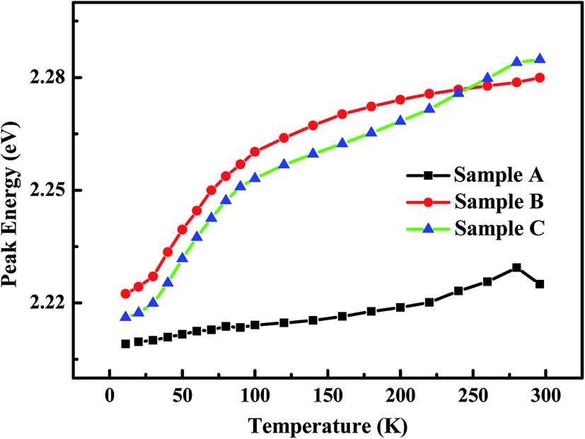 | ||
| Fig. 5 The peak energies of the TD-PL spectra. | ||
To further investigate the carrier localization effects of the three samples, the variation of the normalized integrated PL intensity with temperature was extracted and was fitted using the following Arrhenius equation:36–38
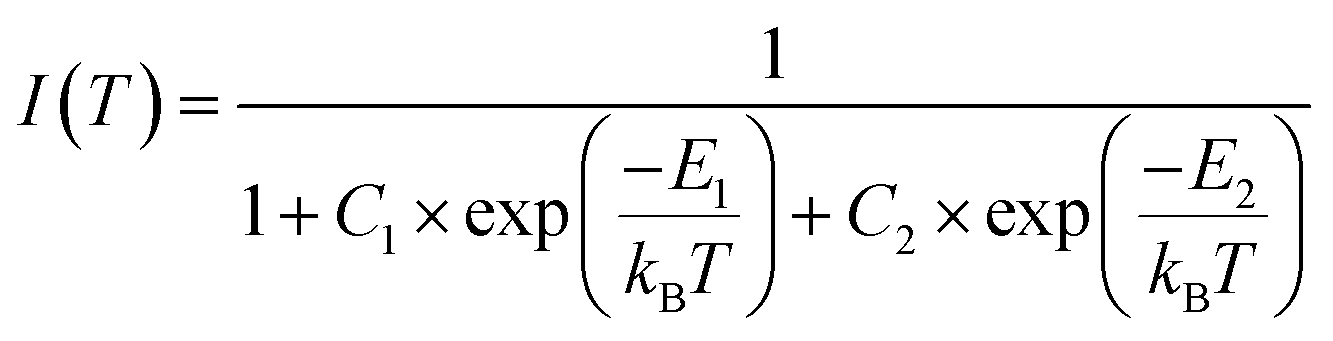 | (1) |
The fitting results are listed in Table 1, and the IQE is calculated by the I300 K/I10 K ratio, assuming that the NRRCs are frozen at 10 K.40 All three E2 values are larger than 60 meV, which are much larger than those in previous reports on InGaN/GaN QWs,33,34 quantificationally proving that the hybrid structures have stronger localization effects than the QWs. E2 of A is larger than that of B and C, confirming the above qualitative assumption. The value of C2 decreases as the GaN barrier thickness increases, indicating that the density of NRRCs is reduced on account of the relieved strain accumulation and relaxation; correspondingly, the IQE is improved.
| Sample | C1 | E1 (meV) | C2 | E2 (meV) | I300 K/I10 K |
|---|---|---|---|---|---|
| A | 2.84 | 12.32 | 110.79 | 69.89 | 7.6% |
| B | 3.04 | 10.25 | 85.40 | 63.12 | 8.4% |
| C | 3.48 | 11.73 | 76.94 | 61.99 | 9.3% |
E2 may be the energy at which a carrier thermally escapes from the localized states. Localized states may form in the QDs due to the high density of VPs or the formation of In-rich QDs in the process of indium phase separation.14 QDs caused by VPs can be observed in the EDS mappings shown in Fig. 3(b), (d) and (f). The formation of In-rich QDs can be attributed to the compositional fluctuation of indium in the InGaN alloy due to indium phase separation and thickness fluctuation of the InGaN well layer. As shown in Fig. 2(a), the InGaN/GaN interfaces of Sample A become ambiguous and the indium distribution becomes inhomogeneous with increasing period. In Fig. 2(b) and (c), the InGaN/GaN interfaces remain sharp as the period increases, and only the VPs increase. Sample A has the highest strain relaxation degree of 8.2%, inducing the strongest indium phase separation41 and ambiguous interfaces. Conversely, Sample C has the lowest strain relaxation degree of 4.1% and sharp interfaces. The strain effect suppresses the process of indium phase separation;42 accordingly, the localization effect of C is weaker than that of A. The strain relaxation degree of B is between those of A and C; thus, the localization effect of B is also in-between. The trend is consistent with the change of E2. In contrast to the trend of E2, the IQE increases from 7.6% (A) to 8.4% (B) to 9.3% (C). Given this, it can be thought that for the three samples, the carrier localization effect is not a major factor in improving the radiative recombination and IQE. In the next section, the effects of defects on the radiative recombination will be discussed, and it will be found that fewer NRRCs due to lower strain relaxation may be the main factor which generates higher IQE.
4. Reduced defects with increasing barrier thickness
C2 is related to the density of NRRCs activated in the high temperature range. As the thickness of the barrier increases, the reduced C2 indicates that the density of NRRCs decreases. This trend is consistent with the relaxation degrees of all three samples. A higher relaxation degree means that more defects (including dislocations, trenches and stacking faults) are generated and act as NRRCs.42,43 As is well known, VPs originate from dislocations, and it has been proved that dislocations can be screened by strong localization effects.12,13 Trench defects were not found by AFM and TEM measurements; therefore, stacking faults may be the major NRRCs. On the other hand, defects in QDs or In-rich areas may be the primary NRRCs, as carriers can be confined and recombination can occur in these defects due to CLE. In order to observe the NRRCs intuitively, HRTEM images of all three samples are shown in Fig. 6. Fig. 6(a) shows the HRTEM image of an island of A. In this island, the last InGaN well is cut into a QD; correspondingly, two areas of the QD were marked as areas 1 and 2 and treated as (0001) lattice plane Bragg filtered images, as shown in Fig. 6(g) and (h). Fig. 6(b) is the HRTEM image of the 2nd and 3rd InGaN wells of A. Two In-rich areas are marked as areas 3 and 4, and their (0001) lattice plane Bragg filtered images are shown in Fig. 6(i) and (j). Similarly, Fig. 6(c) and (d) show the V-shaped pit area and the 2nd and 3rd InGaN wells of B; the (0001) lattice plane Bragg filtered images of areas 5–8 are shown in (k), (l), (m) and (n). Fig. 6(e) and (f) show the V-shaped pit area and the 2nd and 3rd InGaN wells of C, and the (0001) lattice plane Bragg filtered images of area 9–12 are shown in (o), (p), (q) and (r). For A, a large number of stacking faults can be seen in the In-rich areas, as indicated by black arrows, and apparent lattice distortion exists in the whole In-rich areas. Sample B has fewer stacking faults than A, and the lattice distortion is weakened; Sample C contains the fewest stacking faults, and lattice distortion only occurs in local areas where stacking faults are concentrated together. In addition, the thicknesses of the GaN barriers between the 2nd and 3rd InGaN wells are labelled in Fig. 6(b), (d) and (f). The thicknesses (A: 14 nm, B: 16.5 nm, C: 17.2 nm) are smaller than their nominal thicknesses, because areas 1–12 are all In-rich areas and are thicker than the average thicknesses of the InGaN layers due to indium segregation, resulting in reduced barrier thicknesses. According to previous research,43,44 stacking faults can act as NRRCs. The order of the number of stacking faults is A > B > C, especially in the QDs or In-rich areas. This may be the major reason that the IQE are in the order of A < B < C.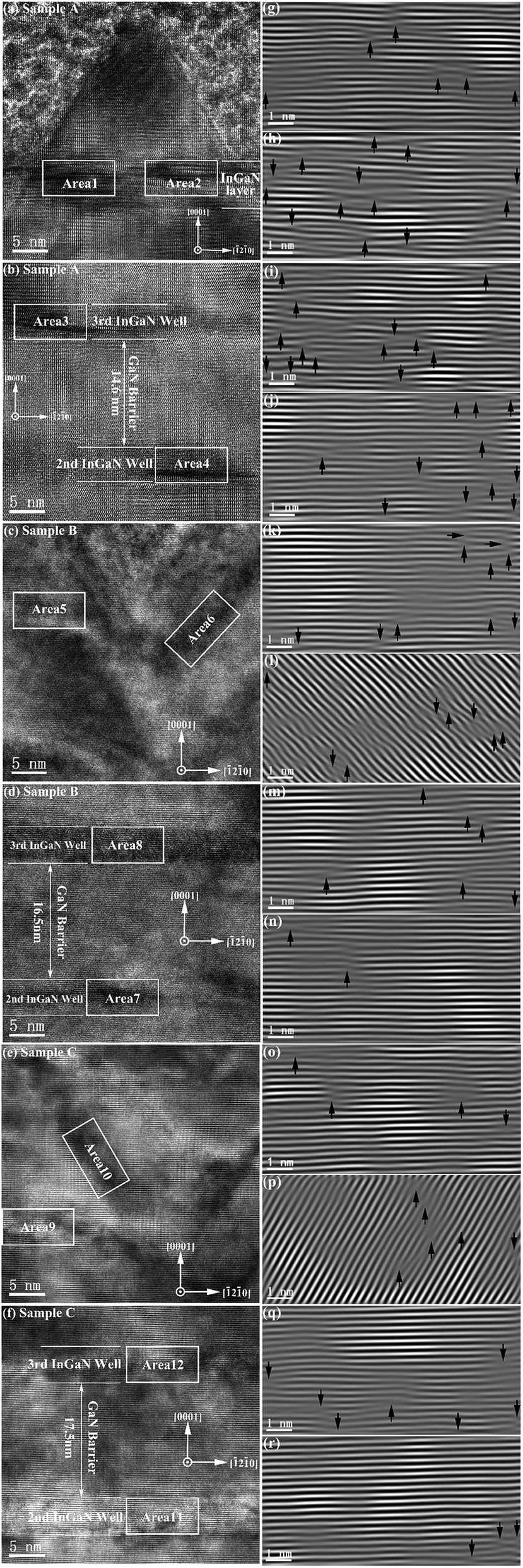 | ||
| Fig. 6 The HRTEM images of (a) an island of A; (b) the 2nd and 3rd InGaN wells of A; (c) a V-shaped pit area of B; (d) the 2nd and 3rd InGaN wells of B; (e) a V-shaped pit area of C; and (f) the 2nd and 3rd InGaN wells of C. (g)-(r) The amplified areas 1–8 processed by the inverse FFT method along the (0001) orientation. | ||
Through comprehensive analysis of the AFM, TEM, HAADF, EDPP-PL, TD-PL and HRTEM data, Sample A shows the highest accumulated strain, which is relaxed by VPs, the most stacking faults and the worst lattice distortion, leading to the highest strain relaxation degree of 8.2%, the strongest CLE and low internal strain, as shown in Fig. 4 and Table 1. The accumulated strain of B is close to that of A because the layer thicknesses of B are more similar to those of A than of C; however, the fewest and the shallowest VPs, fewer stacking faults and smaller lattice distortion cannot relax strain effectively, so a high internal strain remains, inducing the strongest piezoelectric polarization effect and weaker CLE, as analyzed by EPDD-PL (Fig. 4) and TD-PL (Table 1). For Sample C, the thickest barriers isolate the interactions between the InGaN wells, the accumulated strain becomes very low, and the largest and deepest VPs can relax the strain effectively. Although the strain relaxation degree of 4.1% is the lowest, the residual internal strain is still the lowest, and the CLE is the weakest.
Conclusion
In conclusion, three QD/QW structures with different GaN barrier thicknesses of 15 nm (Sample A), 17.5 nm (Sample B) and 20 nm (Sample C) have been grown with MOCVD. A high density of VPs formed during the growth of the InGaN/GaN QWs, and the InGaN wells were cut into QDs by threading dislocations. As the GaN barrier thickness increases, the strain accumulation, strain relaxation degree and carrier localization effects are relieved, and the most important effect is that the density of non-radiative recombination centers in the In-rich areas decreases due to the reduction of the relaxation degree. Although the localized states weaken slightly as the barrier thickness increases, they are still strong enough to confine carriers even at room temperature. By analyzing the strain accumulation and relaxation, the variation of strain field and the carrier localization effect, it can be concluded that the improved IQE is mainly due to the reduction of NRRCs.Conflicts of interest
There are no conflicts to declare.Acknowledgements
This study was funded by the National Key R&D Program of China (2016YFB0401803), the National Natural Science Foundation of China (21972103, 61904120, 61604104, 61805168 and 51672185), Program for Science and Technology Development of Shanxi (201603D121017), Natural Science Foundation of Shanxi Province (201801D221183, 201801D221124, 201801D121101, 201901D111127, 201901D111111, 201901D211090), and the Key Shanxi Provincial R&D Program (201803D31042).References
- S. Nakamura, M. Senoh, N. Iwasa and S.-i. Nagahama, High-brightness InGaN blue, green and yellow light-emitting diodes with quantum well structures, Jpn. J. Appl. Phys., 1995, 34(7A), L797 CrossRef CAS.
- M. X. Feng, J. P. Liu and S. M. Zhang, et al., Design considerations for GaN-based blue laser diodes with InGaN upper waveguide layer, IEEE J. Sel. Top. Quantum Electron., 2013, 19(4), 1500705 Search PubMed.
- J. Liu, Z. Li and L. Zhang, et al., Realization of InGaN laser diodes above 500 nm by growth optimization of the InGaN/GaN active region, Appl. Phys. Express, 2014, 7(11), 111001 CrossRef.
- Y. Jiang, Y. Li and Y. Li, et al., Realization of high-luminous-efficiency InGaN light-emitting diodes in the “green gap” range, Sci. Rep., 2015, 5, 10883 CrossRef CAS.
- S. Saito, R. Hashimoto and J. Hwang, et al., InGaN light-emitting diodes on c-face sapphire substrates in green gap spectral range, Appl. Phys. Express, 2013, 6(11), 111004 CrossRef.
- T. Mukai, M. Yamada and S. Nakamura, Characteristics of InGaN-based UV/blue/green/amber/red light-emitting diodes, Jpn. J. Appl. Phys., 1999, 38(7R), 3976 CrossRef CAS.
- T. Takeuchi, S. Sota and M. Katsuragawa, et al., Quantum-confined Stark effect due to piezoelectric fields in GaInN strained quantum wells, Jpn. J. Appl. Phys., 1997, 36(4A), L382 CrossRef CAS.
- S. De, A. Layek and S. Bhattacharya, et al., Quantum-confined stark effect in localized luminescent centers within InGaN/GaN quantum-well based light emitting diodes, Appl. Phys. Lett., 2012, 101(12), 121919 CrossRef.
- S. Nakamura, The roles of structural imperfections in InGaN-based blue light-emitting diodes and laser diodes, Science, 1998, 281(5379), 956–961 CrossRef CAS.
- S. Nakamura, M. Senoh and S. Nagahama, et al., Continuous-wave operation of InGaN multi-quantumwell-structure laser diodes at 233 K, Appl. Phys. Lett., 1996, 69(20), 3034–3036 CrossRef CAS.
- Y. Xing, D. Zhao and D. Jiang, et al., Carrier Redistribution Between Two Kinds of Localized States in the InGaN/GaN Quantum Wells Studied by Photoluminescence, Nanoscale Res. Lett., 2019, 14(1), 88 CrossRef.
- Y. Narukawa, Y. Kawakami and S. Fujita, et al., Recombination dynamics of localized excitons in In0.20Ga0.80N-In0.05Ga0.95N multiple quantum wells, Phys. Rev. B: Condens. Matter Mater. Phys., 1997, 55(4), R1938 CrossRef CAS.
- Y. Narukawa, Y. Kawakami and M. Funato, et al., Role of self-formed InGaN quantum dots for exciton localization in the purple laser diode emitting at 420 nm, Appl. Phys. Lett., 1997, 70(8), 981–983 CrossRef CAS.
- C. Tessarek, S. Figge and T. Aschenbrenner, et al., Strong phase separation of strained InxGa1−xN layers due to spinodal and binodal decomposition: Formation of stable quantum dots, Phys. Rev. B: Condens. Matter Mater. Phys., 2011, 83(11), 115316 CrossRef.
- L. Wang, W. Lv, H. Zhibiao and Yi Luo, Recent progresses on InGaN quantum dot light-emitting diodes, Frontiers of Optoelectronics, 2014, 7(3), 293–299 CrossRef.
- W. Lv, L. Wang, L. Wang, Y. Xing, Di Yang, H. Zhibiao and Y. Luo, InGaN quantum dot green light-emitting diodes with negligible blue shift of electroluminescence peak wavelength, Appl. Phys. Express, 2014, 7(2), 025203 CrossRef.
- S. H. Park, W. P. Hong and J. J. Kim, Characteristics of built-in polarization potentials in vertically and laterally arranged InGaN/GaN quantum dots, J. Appl. Phys., 2012, 112(12), 123107 CrossRef.
- G. E. Weng, W. R. Zhao and S. Q. Chen, et al., Strong localization effect and carrier relaxation dynamics in self-assembled InGaN quantum dots emitting in the green, Nanoscale Res. Lett., 2015, 10(1), 31 CrossRef.
- J. Liu, Z. Jia and S. Ma, et al., Enhancement of carrier localization effect and internal quantum efficiency through In-rich InGaN quantum dots, Superlattices Microstruct., 2018, 113, 497–501 CrossRef CAS.
- D. J. Kim, Y. T. Moon and K. M. Song, et al., Structural and optical properties of InGaN/GaN multiple quantum wells: The effect of the number of InGaN/GaN pairs, J. Cryst. Growth, 2000, 221(1–4), 368–372 CrossRef CAS.
- S. Pereira, M. R. Correia and E. Pereira, et al., Degradation of structural and optical properties of InGaN/GaN multiple quantum wells with increasing number of wells, Phys. Status Solidi C, 2003,(1), 302–306 CrossRef.
- N. Nuntawong, J. Tatebayashi and P. S. Wong, et al., Localized strain reduction in strain-compensated InAs/GaAs stacked quantum dot structures, Appl. Phys. Lett., 2007, 90(16), 163121 CrossRef.
- H. K. Cho, J. Y. Lee and C. S. Kim, et al., Influence of strain relaxation on structural and optical characteristics of InGaN/GaN multiple quantum wells with high indium composition, J. Appl. Phys., 2002, 91(3), 1166–1170 CrossRef CAS.
- K. Anazawa, S. Hassanet and K. Fujii, et al., Growth of strain-compensated InGaN/AlN multiple quantum wells on GaN by MOVPE, J. Cryst. Growth, 2013, 370, 82–86 CrossRef CAS.
- N. Nuntawong, S. Birudavolu and C. P. Hains, et al., Effect of strain-compensation in stacked 1.3μm InAs/GaAs quantum dot active regions grown by metalorganic chemical vapor deposition, Appl. Phys. Lett., 2004, 85(15), 3050–3052 CrossRef CAS.
- R. A. Oliver, M. J. Kappers and C. J. Humphreys, et al., Growth modes in heteroepitaxy of InGaN on GaN, J. Appl. Phys., 2005, 97(1), 013707 CrossRef.
- J. P. Ahl, J. Hertkorn and H. Koch, et al., Morphology, growth mode and indium incorporation of MOVPE grown InGaN and AlInGaN: a comparison, J. Cryst. Growth, 2014, 398, 33–39 CrossRef CAS.
- P. H. Weidlich, M. Schnedler and H. Eisele, et al., Evidence of deep traps in overgrown v-shaped defects in epitaxial GaN layers, Appl. Phys. Lett., 2013, 103(6), 062101 CrossRef.
- F. Lin, N. Xiang and P. Chen, et al., Investigation of the V-pit related morphological and optical properties of In GaN/GaN multiple quantum wells, J. Appl. Phys., 2008, 103(4), 043508 CrossRef.
- J. H. Ryou, P. D. Yoder and J. Liu, et al., Control of quantum-confined stark effect in InGaN-based quantum wells, IEEE J. Sel. Top. Quantum Electron., 2009, 15(4), 1080–1091 CAS.
- N. G. Young, R. M. Farrell and S. Oh, et al., Polarization field screening in thick (0001) InGaN/GaN single quantum well light-emitting diodes, Appl. Phys. Lett., 2016, 108(6), 061105 CrossRef.
- H. Wang, Z. Ji and S. Qu, et al., Influence of excitation power and temperature on photoluminescence in InGaN/GaN multiple quantum wells, Opt. Express, 2012, 20(4), 3932–3940 CrossRef CAS.
- T. Lu, Z. Ma and C. Du, et al., Temperature-dependent photoluminescence in light-emitting diodes, Sci. Rep., 2014, 4, 6131 CrossRef CAS.
- Y. H. Cho, G. H. Gainer and A. J. Fischer, et al., “S-shaped” temperature-dependent emission shift and carrier dynamics in InGaN/GaN multiple quantum wells, Appl. Phys. Lett., 1998, 73(10), 1370–1372 CrossRef CAS.
- W. Liu, D. G. Zhao and D. S. Jiang, et al., Temperature dependence of photoluminescence spectra for green light emission from InGaN/GaN multiple wells, Opt. Express, 2015, 23(12), 15935–15943 CrossRef CAS.
- L. Liu, L. Wang and D. Li, et al., Influence of indium composition in the prestrained InGaN interlayer on the strain relaxation of InGaN/GaN multiple quantum wells in laser diode structures, J. Appl. Phys., 2011, 109(7), 073106 CrossRef.
- T. Li, A. M. Fischer and Q. Y. Wei, et al., Carrier localization and nonradiative recombination in yellow emitting InGaN quantum wells, Appl. Phys. Lett., 2010, 96(3), 351 Search PubMed.
- Z. Deng, Y. Jiang and Z. Ma, et al., A novel wavelength-adjusting method in InGaN-based light-emitting diodes, Sci. Rep., 2013, 3, 3389 CrossRef.
- T. H. Ngo, B. Gil and P. Valvin, et al., Internal quantum efficiency in yellow-amber light emitting AlGaN-InGaN-GaN heterostructures, Appl. Phys. Lett., 2015, 107(12), 122103 CrossRef.
- J. S. Hwang, A. Gokarna and Y. H. Cho, et al., Direct comparison of optical characteristics of InGaN-based laser diode structures grown on pendeo epitaxial GaN and sapphire substrates, Appl. Phys. Lett., 2007, 90(13), 131908 CrossRef.
- S. Y. Karpov, MRS Internet Journal of Nitride Semiconductor Research., 1998, 3, 16 CrossRef; X. H. Wang, et al., Appl. Phys. Lett., 2009, 94, 111913 CrossRef.
- X. H. Wang, L. W. Guo and H. Q. Jia, et al., Control performance of a single-chip white light emitting diode by adjusting strain in InGaN underlying layer, Appl. Phys. Lett., 2009, 94(11), 111913 CrossRef.
- J. Song, J. Choi and C. Zhang, et al., Elimination of Stacking Faults in Semipolar GaN and Light-Emitting Diodes Grown on Sapphire, ACS Appl. Mater. Interfaces, 2019, 11(36), 33140–33146 CrossRef CAS.
- F. Steib, T. Remmele and J. Gülink, et al., Defect generation by nitrogen during pulsed sputter deposition of GaN, J. Appl. Phys., 2018, 124(17), 175701 CrossRef.
| This journal is © The Royal Society of Chemistry 2020 |