
 Open Access Article
 This Open Access Article is licensed under a Creative Commons Attribution-Non Commercial 3.0 Unported Licence
Enhanced charge storage properties of ultrananocrystalline diamond films by contact electrification-induced hydrogenation†
Jae-Eun Kim ab,
Kalpataru Pandaa and
Jeong Young Park*ab
ab,
Kalpataru Pandaa and
Jeong Young Park*ab
aCenter for Nanomaterials and Chemical Reactions, Institute for Basic Science (IBS), Daejeon 34141, Republic of Korea. E-mail: jeongypark@kaist.ac.kr
bDepartment of Chemistry, Korea Advanced Institute of Science and Technology (KAIST), Daejeon 34141, Republic of Korea
First published on 8th September 2020
Abstract
We report the enhanced charge storage characteristics of ultrananocrystalline diamond (UNCD) by contact electrification-induced hydrogenation. The non-catalytic hydrogenation of UNCD films was achieved by using platinum as an electron donor and sulfuric acid as a hydrogen proton donor, confirmed by Raman spectroscopy and time-of-flight secondary ion mass spectroscopy (TOF-SIMS). Chemical treatment with only a H2SO4 solution is responsible for the surface oxidation. The oxidation of UNCD resulted in an increase in the quantity and duration of the tribocharges. After non-catalytic hydrogenation, the generation of friction-induced tribocharges was enhanced and remained for three hours and more. We show that the hydrogen incorporation on grain boundaries is responsible for the improvement of charge storage capability, because the doped hydrogen acts as a trap site for the tribocharges. This lab-scale and succinct method can be utilized to control charge trap capability in nanoscale memory electronics.
Introduction
Ultrananocrystalline diamond (UNCD), diamond films fabricated by chemical vapor deposition (CVD), is composed of sp3-bonded grains and graphitic grain boundaries containing hydrocarbons.1 These diamond films are chemically inert, mechanically stiff, and extremely hard.2–4 Furthermore, since UNCD has defects like grain boundaries, the electrical properties (e.g., conductivity and field emission) can be tuned via atomic doping.5–7 Under conditions where periodic mechanical contact between widely used materials (e.g., silicon) occurs, plastic deformation due to friction can be problematic for their effective use; still, UNCD has a low coefficient of friction compared to Si and other materials.4,8 In addition, there have been many efforts to use UNCD for micro-electro-mechanical systems (MEMS) as a dielectric material.9 Because of these advantages, UNCD has many potential applications in small electronic devices under harsh conditions.Chemical modification, including oxidation and hydrogenation, is a widely used method for controlling mechanical and electrical properties of various materials, including two dimensional sheets or nanowires.10–13 In the case of UNCD, the material properties can be tuned by affecting crystal structure-inducing lattice distortion14,15 and the band structure of graphene-donating extra carriers.16,17 Furthermore, transition behavior can be controlled via atomic hydrogen incorporation; in the presence of hydrogen atoms in the matrix, the metallic phase does not transfer to the semiconducting phase and remains stable at room temperature due to hydrogen atoms.18–20 Hydrogen content, while fabricating diamond films with CVD, plays a critical role in establishing nucleation between the UNCD and the substrate.21 For instance, the microstructure of UNCD was investigated by controlling the composition of gas during deposition. As the ratio of hydrogen to argon decreases, so does the grain size of UNCD films.22 Roughness also decreases with lower hydrogen content. Raman spectroscopy sheds light on the structural changes due to hydrogen atoms in diamond films, because it allows for direct observation of C–H bonds.23,24 The incorporated hydrogen atoms in the grain boundaries of UNCD films have an impact on their electrical conductivity, passivating dangling bonds of graphitic carbons and unsaturated hydrocarbons.25
Both electrical conductance and charge storage characteristics could be affected by atomic doping.26,27 The charges generated by the friction of two different materials are referred to as tribocharges. The practicability of using harvested tribocharges converted from mechanical energy was demonstrated by Z. L. Wang et al., by making triboelectric nanogenerators (TENGs).28,29 The discovery of the TENG has an impact on the field of self-powered systems, suggesting eco-friendly, repetitive, and easy-to-fabricate methods.30 It has been shown that modification (e.g., surface roughening,31 oxidation,32 functionalization33) on the surface effectively improves the performance of TENGs. For this reason, it is important to obtain a comprehensive understanding of the chemistry of the surfaces that are directly relevant to tribocharging properties through atomic force microscopy (AFM), which enables nanometer-scale research.33–37 Atomic doping has been shown to be a feasible and effective way to improve the electrical properties38–40 and charge trapping properties27 of UNCD. By utilizing such methods, atomic doping was carried out during deposition process, morphologies, chemical composition, and grain size was also affected. Furthermore, the overall bulk characteristics change, since doping occurs during the deposition process.
In this study, we have demonstrated the non-catalytic hydrogenation on UNCD and improved charge storage properties of UNCD films via atomic incorporation. The hydrogenation is called electron–proton co-doping, which is a feasible way to control the electrical behavior of oxide materials. The hydrogenation varied the electrical, (e.g., conductance and work function), physical, and/or chemical properties (e.g., friction and adhesion). We confirmed whether or not hydrogenation occurred using Raman spectroscopy and TOF-SIMS measurements. After hydrogenation, the quantity of tribocharges increased by a factor of 2.5. More interestingly, the durability, as well as the number, of tribocharges were noticeably enhanced. This enhancement is presumably due to the passivation of carbons at the grain boundaries. The lack of dangling bonds resulted in a decrease in conductance, so the tribocharges of hydrogenation UNCD can survive longer than that of bare UNCD.
Experimental
Sample preparation
We used UNCD wafers fabricated with microwave-CVD using an Ar-rich/CH4 mixed precursor on a Si wafer with a thickness of 200 nm (UA25-100-1-p2, Advanced Diamond Technologies). We prepared three different samples for an accurate comparison: bare UNCD without any chemical treatment, oxidized UNCD, which is UNCD immersed in 2 wt% sulfuric acid for three hours, and hydrogenated UNCD prepared by contact electrification-induced hydrogenation. For simplicity, the pristine, surface oxidized, and hydrogenated UNCD films are designated UNCD, O-UNCD, and H-UNCD, respectively. The morphologies of the samples were observed with FE-SEM as can be seen in Fig. S1(a)–(c).† For the last sample, a platinum film with a thickness of 50 nm (Fig. S1(d)†) was deposited by e-beam evaporation at the basal pressure of 1 × 10⁻⁶ Torr with a deposition rate of 1 Å s−1 on UNCD films fabricated by a microwave-assisted chemical vapor deposition method.1 After the deposition of Pt on part of the UNCD using a 2 × 2 cm2 square-patterned shadow mask, we put the sample in 2 wt% sulfuric acid for three hours in order to incorporate hydrogen atoms within UNCD. To clean the residue from the sulfuric acid, the UNCD films were rinsed with DI water. Furthermore, in order to rule out the effect of adsorbed water, not only sulfuric acid treated UNCD films but bare UNCD films were cleaned with DI water, followed by drying with N2 gas. The process is presented in Fig. 1 in detail. | ||
| Fig. 1 Schematic diagram of contact electrification-induced hydrogenation of UNCD. | ||
Characterization
The morphologies, roughness, and contact potential difference (CPD) were measured using interleave mode Kelvin probe force microscopy (KPFM), which can measure topography and surface potential simultaneously without an artifact resulting from height difference, since the tip explores the surface of the sample, maintaining tip-sample distance.10 The fast scan axis size is 500 nm, and a tip velocity was 0.5 Hz for the samples. The commercial Pt/Ir coated cantilever (PPP-EFMR, Nanosensors) was used for the characterization. The root mean square roughness was calculated as described elsewhere.41 Furthermore, for the qualitative and structural analysis, we carried out Raman spectroscopy (LabRAM HR Evolution Visible_NIR, Horiba). We used the He–Ne laser with excitation frequency of 633 nm that can excite sp2 site with lower band gap for UNCD, O-UNCD and H-UNCD. Time-of-flight secondary ion mass spectroscopy (TOF-SIMS) (TOF-SIMS5, Ion-TOF GmbH) equipped with a bismuth liquid metal ion gun (LMIG) measurements were carried out. For each measurement, positive mode was conducted over a 300 × 300 μm2 area at a resolution of 256 × 256 pixels using primary ion at 30 keV with a pulse width of 35 ns. A flood gun was used for charge neutralization for the analysis. In order to measure work function, ultraviolet photoelectron spectroscopy (UPS) (Sigma Probe, Thermo VG Scientific) measurements were carried out in an ultra-high vacuum (UHV) irradiating photons with 21.22 eV applying a sample bias of −5 V for the cut-off region of secondary electrons. The work function (φ) was obtained by subtracting the difference between the cut-off energy (Ecut-off) with the Fermi edge energy (EF) from He I line energy (φ = 21.22 − (Ecut-off – EF) eV).Charge writing and reading process
In order to avoid wear and damage from the friction force while scanning the surface with physical contact and forming tribocharges, a diamond-coated cantilever (CDT-CONTR, Nanosensors) was used to generate tribocharges and measure the properties including morphologies, friction, adhesion, and tribocharges. The charges were formed by scratching the surface of 500 × 500 nm2 area with a diamond-coated cantilever, with a scan speed of 1 Hz, applying normal forces of 30, 60 and 90 nN at different sites using general contact mode AFM. Immediately after creating the charges, we measured the surface potential of the samples with KPFM mode AFM. The nominal spring constant and resonance frequency of diamond-coated cantilever is 6.2 N m−1 and 105 kHz. The 20 × 20 um2 area was scanned with a tip velocity of 0.3 Hz, maintaining a tip height of 30 nm. The duration of the generated tribocharges was recorded by continuously scanning the CPD of the samples.Results and discussion
Fig. 1 represents a schematic of contact electrification-induced hydrogenation of UNCD, using Pt as a provider of electrons and sulfuric acid to supply hydrogen ions. When the UNCD and e-beam evaporated Pt with a thickness of 50 nm make contact with each other, contact electrification occurs. Due to the contact between Pt and UNCD, the contact electrification-induced electrons from the metal were generated and then accumulated at the surface of UNCD. Making contact with the UNCD surface with a Pt coated tip increases the contact potential difference (CPD) at the contact area, indicating that the surface of UNCD is negatively charged, and Pt is positively charged, as confirmed by the writing and reading process by carrying out contact mode AFM and KPFM (Fig. S2†). The result implies that the electrons were transferred from the Pt to the UNCD surface. Immediately following the deposition, the sample was immersed in 2 wt% sulfuric acid for 3 h. Consequently, the hydrogen ions originating from dissolved sulfuric acid were attracted by the doped electrons, and the electrons reacted and formed hydrogen atoms at the interface of Pt and the UNCD. The hydrogen atoms were repeatedly generated around the surface of UNCD. Because of this behavior, the insulating surface could undergo a transition to metallic phase. The co-doping occurs mainly at the grain boundaries, mostly composed of sp3 bonding, and the repeated cycles hydrogenate the UNCD surface entirely. Y. Chen et al., reported a non-catalytic hydrogenation method for VO2. In the procedure, electrons from the metal to VO2 were moved by work function difference, and the electrons and protons in sulfuric acid formed atomic hydrogens, a process called contagious electron–proton co-doping.42 Fundamentally, the doping mechanism is the same, but in our system, the basis of the movement of electrons is the contact electrification in the metal–insulator interface, not the difference in work function between Pt and UNCD. Generally, the electron could transfer from low work function metal to high work function metal, but this tendency is not absolute. The driving force of electron drift is still unclear in the case of metal-to-insulator interface.43,44 The surface of UNCD became oxidized by sulfuric acid, as confirmed by XPS measurements showing an increase in atomic oxygen ratio with respect to the atomic carbon ratio, and the oxidation occurred at the surface of O-UNCD and H-UNCD (Fig. S3†). Fig. 2 shows the morphologies and surface potentials of UNCD samples. AFM topographical images and FE-SEM images (Fig. S1(a)–(c)†) indicated that the oxidation and hydrogenation did not affect morphological properties. Even in XRD results, there was no significant change in crystallinity exhibiting the (111) crystallographic plane of diamond structure (Fig. S4†). It was shown that the grain size is around 20 nm, as depicted in morphologies, and the roughness of UNCD films is around 6 nm (Fig. 2(d)), which is consistent with the previous results observed by AFM.3 It is obvious that the crystallinity of UNCD exhibiting sp3-bonded carbon (111) reflection did not vary due to the chemical treatment using sulfuric acid. While the morphologies were not affected by sulfuric acid and hydrogenation, surface potential decreased after the chemical treatment (Fig. 2(a)–(c)). From the results of surface potential measurements as seen in Fig. 2, it can be predicted that work function increases by oxidation and hydrogenation. The increment was double-checked using UPS, exhibiting that the work function increased from 4.02 to 4.37 and 4.49 eV because of oxidation and hydrogenation, respectively (Fig. S5†). It can be assumed that the increase of work function was mainly due to sulfuric acid, since the dramatic increase in work function was observed in O-UNCD, and the atomic oxygen ratio was double. Cleaning the carbon-contaminated surface and oxidation contributed to the variance.45 It should be noted that, although it seems that work function increased significantly more due to hydrogenation, the films were exposed to air, so there might be some alterations in work function values (less than 0.2 eV is possible).46 As seen in the work by Cui et al., hydrogen affects field emission properties because of contributions to reduce the emission barrier by decreasing the electron affinity of the surface,47 but hydrogen concentration has little impact on the surface potential (i.e., work function) of UNCD samples.25 On the other hand, it has been stated that the termination of CVD grown diamond surface with oxygen and hydrogen results in an increase in work function. The surface potential of the O-terminated diamond is higher than that of the H-terminated diamond, implying that H-termination increases work function.48 Furthermore, it was inferred from temperature-dependent I–V characteristics in the Schottky contact in hydrogenated samples that shallow acceptors exist in the subsurface.49 It means that the Fermi level decreased, resulting in an increase in work function. The electrical properties can be varied by hydrogen incorporation between the grains of diamond thin films, due to dangling bond passivation affecting defect density.50 In addition, the chemical state of the diamond surface changed from the graphitic phase to amorphous, due to excessive H-plasma treatment lowering electrical properties.26 | ||
| Fig. 2 Topography (above) and corresponding surface potential (bottom) of (a) bare UNCD, (b) H2SO4 treated (O-UNCD) and (c) hydrogenated UNCD (H-UNCD). (d) RMS roughness (Rq) calculated from topography, and (e) averaged contact potential difference (CPD) of UNCD, O-UNCD, and H-UNCD. | ||
The extra bonding of hydrogen and carbon was observed by Raman spectra and TOF-SIMS measurements. Generally, D- and G-resonance bands could be found at ∼1350 and 1550 cm−1 in Raman, which are indications of sp2-bonded carbons. The peaks were assigned not to sp3-bonded phases but to sp2-bonded carbons, because the intensity of the peaks decreased with excitation wavelength, and the behavior is consistent with the results of sp2 bond assigning peak. The G peak corresponds to a vibration of bond-stretching of sp2 pairs. The disordering of sp2 and some defects are relevant to D peak. Furthermore, D* resonance peak is associated with sp3 bondings (diamond phase) and the intensity of the band could increase with the excitation energy.51 Herein, it is not possible to deconvolute D and D* bands, because we used a visible laser for sensitivity to acquire sp2 bonding peak. The sensitivity to sp2 bonding is several times the sensitivity to sp3 bonding. It is assumed that the slight increase in D peak of O-UNCD and H-UNCD with respect to that of UNCD is a result of defects from the sulfuric acid treatment. Most importantly, we assigned two peaks as the evidence of additional C–H bonding in UNCD at ∼1140 (ν1) and 1450 cm−1 (ν3) in Fig. 3(a).24 These two peaks are associated with hydrocarbons in the form of tranpolyacetylene (t-PA) at the grain boundaries of nanocrystalline CVD diamonds.52–54 The peak broadening of D and G bands are the result of the evolution of t-PA resonance peak and surface oxidation. For a quantitative comparison of incorporated hydrogen atoms, the intensity of peaks indicating the mass of H and CnHn at O-UNCD, and H-UNCD was normalized by the peak intensity of bare UNCD underlying the results in Fig. S6.† Furthermore, as can be seen in Fig. 3(b), the quantity of C6Hn bonds increased in H-UNCD. Note that the hydrogen atoms were mainly detected as atomic hydrogen and C6Hn. On the basis of these results, we can speculate that the hydrogenation takes place at the sp2 bonded graphitic carbons, which are mainly in grain boundaries accompanying small amounts of hydrogen incorporation.
 | ||
| Fig. 3 (a) Raman spectrum of UNCD, O-UNCD, and H-UNCD. The arrows in (a) imply that the C–H bonds were generated because of hydrogenation. (b) Normalized intensity of the amount of hydrogen and ratio of CxHn with respect to Cx obtained from TOF-SIMS measurements measured on UNCD, O-UNCD, and H-UNCD. | ||
Fig. 4 shows the tribocharging properties of UNCD films. Changes in morphology due to sulfuric acid and hydrogenation were not found, and wear resulting from rubbing with a diamond tip did not occur, as shown in 20 μm × 20 μm topography images (Fig. 4(a)–(c)). Fig. 4(d)–(f) exhibit the evolution of tribocharges caused by frictional interaction between an AFM tip and UNCD surfaces. In the surface potential images, brighter contrast at three written areas indicates that the areas were negatively charged by triboelectrification. Compared to the results of tribocharges on UNCD, the brighter areas due to tribocharges, are concentrated near the scratched region and are less dispersed than bare UNCD. It implies that the charges can be more effectively trapped at the surface of oxidized and/or hydrogenated UNCD. From the line profile plots (Fig. 4(g)–(i)) corresponding to the dotted line in Fig. 4(d)–(f), respectively, at the surface of bare UNCD, 29, 33 and 38 mV of tribocharges were generated by friction, applying normal forces of 30, 60 and 90 nN, respectively, exhibiting load dependency. In the case of oxidized UNCD, tribocharges increased to 40, 55 and 59 mV. Furthermore, the hydrogenated UNCD showed about double the improvement of tribocharges by each normal force, compared to the bare UNCD. Therefore, oxidation and hydrogenation are responsible for the improved triboelectric properties of UNCD films. Besides, we could see the clear load dependence of tribocharges at all three samples, as can be seen in the friction as a function of applied loads in Fig. S7.† The friction area is linearly proportional to the friction so that there are more tribocharges when the higher load is applied.28 Since the sliding contact with UNCD and diamond tip exhibited Derjaguin–Muller–Toporove (DMT) model behavior,32 the relationship between the contact area and the load can be expressed as the following equation:55
 | (1) |
 | ||
| Fig. 4 Topography of (a) UNCD, (b) O-UNCD and (c) H-UNCD films. As-rubbed surface potential images of (d) UNCD, (e) O-UNCD and (f) H-UNCD with an applied load of 30, 60 and 90 nN (red, blue and green colored dash line respectively). CPD line profile at dash line in CPD mapping of (g) UNCD, (h) O-UNCD and (i) H-UNCD. | ||
In the equation, A is the effective contact area, when the AFM tip elastically contacts the surface of the sample in single asperity. R is the curvature radius of AFM tip apex. K is the reduced Young's modulus. L is the adhesion force between AFM tip and UNCD and γ is the work of adhesion. For this reason, the load-dependent tribocharges can be explained by this load-dependent frictional behavior. The higher friction forces at O-UNCD and H-UNCD could be one of the possible reasons for the higher production of tribocharges.
Fig. 5 shows the continuously measured KPFM results immediately after the charge writing process, exhibiting the durability of the friction-induced tribocharges of UNCD films. As shown in Fig. 5(a), the charges of bare UNCD were dissipated in 102 min, but a small quantity of charges remained on the oxidized UNCD (Fig. 5(b)). This enhancement was caused by the increased resistance of the oxidized UNCD.28 In the case of H-UNCD, an outstanding increment in charge duration was observable (Fig. 5(c)). Even after 210 min, the CPD of written area was higher by as much as ∼20 mV than that of the unwritten area, indicating that tribocharges were retained for more than 3 h. Furthermore, as can be seen in Fig. 5(d), H-UNCD exhibited not only higher initial tribocharge generation, but longer duration among UNCD samples under a normal force of 90 nN. This phenomenon could also be observed at applied loads of 30 and 60 nN (Fig. S8†). The elongation of duration time is not because of an increased quantity of tribocharges, but because of chemical modification, since the initial decay rate from 0 min up to 68 min on H-UNCD is lower than that of O-UNCD and UNCD, showing the slower decrease in tribocharges. The improvement was caused by two possible effects resulting from hydrogenation. First, after hydrogenation, the surface of the UNCD became more insulative than oxidized and bare UNCD films (Fig. S9†). Sulfuric acid treatment is responsible for the increase of resistance, because the graphitic phase could be cleaned out, and conductive dangling bonds were passivated via oxidation. Second, the incorporated hydrogen atoms and hydrocarbons in grain boundaries can act as charge trapping sites. Atomic doping in UNCD is useful for the charge storage medium to trap tribocharges.27 For this reason, both an increased initial level of tribocharges and a greater duration of the charges of H-UNCD compared to the charge duration of O-UNCD can be achieved.
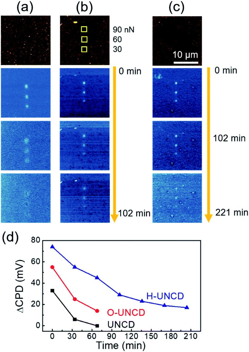 | ||
| Fig. 5 Continuously measured surface potential images of (a) UNCD, (b) O-UNCD and (c) H-UNCD. (d) Charge dissipation as a function of elapse time of UNCD films. | ||
In summary, we have shown that charge storage on UNCD is improved by contact electrification-induced hydrogenation. Hydrogen ions were supplied from the sulfuric acid, and electrons were drifted by contact electrification from metallic Pt, resulting in a non-catalytic hydrogenation of UNCD. We observed the additionally formed carbon–hydrogen interactions in the forms of t-PA and/or hydrocarbons at grain boundaries using Raman spectroscopy and SIMS measurements. We found hydrogen atoms impregnated within grain boundaries, and that the surface oxidation boosted the capacity for tribocharges. Changes in friction-induced charges by the AFM tip were quantitively measured using KPFM. The scratched area became negatively charged, showing relatively brighter contrast in the surface potential image. On the O-UNCD and H-UNCD surfaces, the contrast was more prominent because of the increment of resistance and friction and the charge trapping role of incorporated hydrogen. The chemical modification of UNCD may be useful in controlling charge trap capability with the potential application of nanoscale memory electronics.
Conflicts of interest
There are no conflicts to declare.Acknowledgements
This work was supported by the Institute for Basic Science (IBS) [IBS-R004].References
- A. V. Sumant, D. S. Grierson, J. E. Gerbi, J. A. Carlisle, O. Auciello and R. W. Carpick, Phys. Rev. B: Condens. Matter Mater. Phys., 2007, 76, 235429 CrossRef.
- V. P. Adiga, A. V. Sumant, S. Suresh, C. Gudeman, O. Auciello, J. A. Carlisle and R. W. Carpick, Phys. Rev. B: Condens. Matter Mater. Phys., 2009, 79, 245403 CrossRef.
- J. E. Butler and A. V. Sumant, Chem. Vap. Deposition, 2008, 14, 145–160 CrossRef CAS.
- A. R. Krauss, O. Auciello, D. M. Gruen, A. Jayatissa, A. Sumant, J. Tucek, D. C. Mancini, N. Moldovan, A. Erdemir, D. Ersoy, M. N. Gardos, H. G. Busmann, E. M. Meyer and M. Q. Ding, Diamond Relat. Mater., 2001, 10, 1952–1961 CrossRef CAS.
- O. A. Williams, Semicond. Sci. Technol., 2006, 21, R49–R56 CrossRef CAS.
- J. Birrell, J. A. Carlisle, O. Auciello, D. M. Gruen and J. M. Gibson, Appl. Phys. Lett., 2002, 81, 2235–2237 CrossRef CAS.
- I. S. Beloborodov, P. Zapol, D. M. Gruen and L. A. Curtiss, Phys. Rev. B: Condens. Matter Mater. Phys., 2006, 74, 235434 CrossRef.
- A. R. Konicek, D. S. Grierson, P. U. Gilbert, W. G. Sawyer, A. V. Sumant and R. W. Carpick, Phys. Rev. Lett., 2008, 100, 235502 CrossRef CAS.
- C. Goldsmith, A. Sumant, O. Auciello, J. Carlisle, H. Zeng, J. C. M. Hwang, C. Palego, W. Wang, R. Carpick, V. P. Adiga, A. Datta, C. Gudeman, S. O. Brien and S. Sampath, IEEE MTT-S Int. Microwave Symp. Dig., 2010, 1246–1249 Search PubMed.
- J. E. Kim, J. Y. Shin, H. S. Jang, J. W. Jeon, W. G. Hong, H. J. Kim, J. Choi, G. T. Kim, B. H. Kim, J. Park, Y. J. Choi and J. Y. Park, Nanoscale, 2019, 11, 4219–4225 RSC.
- W. H. Doh, W. Jeong, H. Lee, J. Park and J. Y. Park, Nanotechnology, 2016, 27, 335603 CrossRef.
- J. Huh, J. Park, G. T. Kim and J. Y. Park, Nanotechnology, 2011, 22, 085502 CrossRef.
- J.-H. Ko, S. Kwon, I.-S. Byun, J. S. Choi, B. H. Park, Y.-H. Kim and J. Y. Park, Tribol. Lett., 2013, 50, 137–144 CrossRef CAS.
- D. C. Elias, R. R. Nair, T. M. G. Mohiuddin, S. V. Morozov, P. Blake, M. P. Halsall, A. C. Ferrari, D. W. Boukhvalov, M. I. Katsnelson, A. K. Geim and K. S. Novoselov, Science, 2009, 323, 610–613 CrossRef CAS.
- T. Xia and X. Chen, J. Mater. Chem. A, 2013, 1, 2983 RSC.
- D. Haberer, D. V. Vyalikh, S. Taioli, B. Dora, M. Farjam, J. Fink, D. Marchenko, T. Pichler, K. Ziegler, S. Simonucci, M. S. Dresselhaus, M. Knupfer, B. Buchner and A. Gruneis, Nano Lett., 2010, 10, 3360–3366 CrossRef CAS.
- H. Gao, L. Wang, J. Zhao, F. Ding and J. Lu, J. Phys. Chem. C, 2011, 115, 3236–3242 CrossRef CAS.
- H. Yoon, M. Choi, T. W. Lim, H. Kwon, K. Ihm, J. K. Kim, S. Y. Choi and J. Son, Nat. Mater., 2016, 15, 1113–1119 CrossRef CAS.
- J. Wei, H. Ji, W. Guo, A. H. Nevidomskyy and D. Natelson, Nat. Nanotechnol., 2012, 7, 357–362 CrossRef CAS.
- Y. Filinchuk, N. A. Tumanov, V. Ban, H. Ji, J. Wei, M. W. Swift, A. H. Nevidomskyy and D. Natelson, J. Am. Chem. Soc., 2014, 136, 8100–8109 CrossRef CAS.
- S. Jiao, A. Sumant, M. A. Kirk, D. M. Gruen, A. R. Krauss and O. Auciello, J. Appl. Phys., 2001, 90, 118–122 CrossRef CAS.
- D. Zhou, D. M. Gruen, L. C. Qin, T. G. McCauley and A. R. Krauss, J. Appl. Phys., 1998, 84, 1981–1989 CrossRef CAS.
- S. A. Rakha, C. Jianqing, X. Huihao, Y. Guojun, D. Zhu and J. Gong, Diamond Relat. Mater., 2009, 18, 1247–1252 CrossRef CAS.
- J. Birrell, J. E. Gerbi, O. Auciello, J. M. Gibson, J. Johnson and J. A. Carlisle, Diamond Relat. Mater., 2005, 14, 86–92 CrossRef CAS.
- W. F. Paxton, M. Howell, W. P. Kang and J. L. Davidson, J. Vac. Sci. Technol., B: Nanotechnol. Microelectron.: Mater., Process., Meas., Phenom., 2012, 30, 021202 Search PubMed.
- K. Panda, K. J. Sankaran, B. K. Panigrahi, N. H. Tai and I. N. Lin, ACS Appl. Mater. Interfaces, 2014, 6, 8531–8541 CrossRef CAS.
- K. Panda, J.-E. Kim and J. Y. Park, Carbon, 2019, 141, 123–133 CrossRef CAS.
- G. Zhu, Z. H. Lin, Q. Jing, P. Bai, C. Pan, Y. Yang, Y. Zhou and Z. L. Wang, Nano Lett., 2013, 13, 847–853 CrossRef CAS.
- Z. L. Wang, ACS Nano, 2013, 7, 9533–9557 CrossRef CAS.
- F.-R. Fan, Z.-Q. Tian and Z. Lin Wang, Nano Energy, 2012, 1, 328–334 CrossRef CAS.
- S. Wang, L. Lin and Z. L. Wang, Nano Lett., 2012, 12, 6339–6346 CrossRef CAS.
- J.-E. Kim, K. Panda, J. I. J. Choi and J. Y. Park, Nanoscale, 2019, 11, 6120–6128 RSC.
- J. H. Kim, B. K. Yun, J. H. Jung and J. Y. Park, Appl. Phys. Lett., 2016, 108, 133901 CrossRef.
- H. S. Kim, D. Y. Kim, J. E. Kim, J. H. Kim, D. S. Kong, G. Murillo, G. H. Lee, J. Y. Park and J. H. Jung, Adv. Funct. Mater., 2019, 29, 1905816 CrossRef CAS.
- H.-J. Kim, E.-C. Yim, J.-H. Kim, S.-J. Kim, J.-Y. Park and I.-K. Oh, Nano Energy, 2017, 33, 130–137 CrossRef CAS.
- J. Ha, J. Chung, S. Kim, J. H. Kim, S. Shin, J. Y. Park, S. Lee and J.-B. Kim, Nano Energy, 2017, 36, 126–133 CrossRef CAS.
- H.-J. Kim, J.-H. Kim, K.-W. Jun, J.-H. Kim, W.-C. Seung, O. H. Kwon, J.-Y. Park, S.-W. Kim and I.-K. Oh, Adv. Energy Mater., 2016, 6, 1502329 CrossRef.
- X. J. Hu, J. S. Ye, H. Hu, X. H. Chen and Y. G. Shen, Appl. Phys. Lett., 2011, 99, 131902 CrossRef.
- S. Wang, V. M. Swope, J. E. Butler, T. Feygelson and G. M. Swain, Diamond Relat. Mater., 2009, 18, 669–677 CrossRef CAS.
- K. J. Sankaran, M. Ficek, S. Kunuku, K. Panda, C. J. Yeh, J. Y. Park, M. Sawczak, P. P. Michalowski, K. C. Leou, R. Bogdanowicz, I. N. Lin and K. Haenen, Nanoscale, 2018, 10, 1345–1355 RSC.
- E. S. Gadelmawla, M. M. Koura, T. M. A. Maksoud, I. M. Elewa and H. H. Soliman, J. Mater. Process. Technol., 2002, 123, 133–145 CrossRef.
- Y. Chen, Z. Wang, S. Chen, H. Ren, L. Wang, G. Zhang, Y. Lu, J. Jiang, C. Zou and Y. Luo, Nat. Commun., 2018, 9, 818 CrossRef.
- D. J. Lacks and R. Mohan Sankaran, J. Phys. D: Appl. Phys., 2011, 44, 453001 CrossRef.
- Z. L. Wang and A. C. Wang, Mater. Today, 2019, 30, 34–51 CrossRef CAS.
- S. Y. Kim, J.-L. Lee, K.-B. Kim and Y.-H. Tak, J. Appl. Phys., 2004, 95, 2560–2563 CrossRef CAS.
- M. Vasilopoulou, A. M. Douvas, D. G. Georgiadou, L. C. Palilis, S. Kennou, L. Sygellou, A. Soultati, I. Kostis, G. Papadimitropoulos, D. Davazoglou and P. Argitis, J. Am. Chem. Soc., 2012, 134, 16178–16187 CrossRef CAS.
- J. B. Cui, J. Ristein, M. Stammler, K. Janischowsky, G. Kleber and L. Ley, Diamond Relat. Mater., 2000, 9, 1143–1147 CrossRef CAS.
- M. C. Salvadori, W. W. R. Araújo, F. S. Teixeira, M. Cattani, A. Pasquarelli, E. M. Oks and I. G. Brown, Diamond Relat. Mater., 2010, 19, 324–328 CrossRef CAS.
- K. Hayashi, S. Yamanaka, H. Watanabe, T. Sekiguchi, H. Okushi and K. Kajimura, J. Appl. Phys., 1997, 81, 744–753 CrossRef CAS.
- C. Liu, X. Xiao, J. Wang, B. Shi, V. P. Adiga, R. W. Carpick, J. A. Carlisle and O. Auciello, J. Appl. Phys., 2007, 102, 074115 CrossRef.
- R. Arenal, G. Montagnac, P. Bruno and D. M. Gruen, Phys. Rev. B: Condens. Matter Mater. Phys., 2007, 76, 245316 CrossRef.
- A. C. Ferrari and J. Robertson, Phys. Rev. B: Condens. Matter Mater. Phys., 2001, 63, 121405(R) CrossRef.
- A. T. Sowers, B. L. Ward, S. L. English and R. J. Nemanich, J. Appl. Phys., 1999, 86, 3973–3982 CrossRef CAS.
- T. López-Ríos, É. Sandré, S. Leclercq and É. Sauvain, Phys. Rev. Lett., 1996, 76, 4935–4938 CrossRef.
- J. Y. Park and M. Salmeron, Chem. Rev., 2014, 114, 677–711 CrossRef CAS.
Footnote |
| † Electronic supplementary information (ESI) available. See DOI: 10.1039/d0ra05409g |
| This journal is © The Royal Society of Chemistry 2020 |