
 Open Access Article
 This Open Access Article is licensed under a Creative Commons Attribution-Non Commercial 3.0 Unported Licence
Reactive ion etching of an ovonic threshold switch (OTS) material using hydrogen-based plasmas for non-volatile phase change memories
Doo San Kim a,
Ju Eun Kima,
You Jung Gilla,
Jin Woo Parka,
Yun Jong Janga,
Ye Eun Kima,
Hyejin Choib,
Oik Kwonb and
Geun Young Yeom*ac
a,
Ju Eun Kima,
You Jung Gilla,
Jin Woo Parka,
Yun Jong Janga,
Ye Eun Kima,
Hyejin Choib,
Oik Kwonb and
Geun Young Yeom*ac
aSchool of Advanced Materials Science and Engineering, Sungkyunkwan University, Suwon 16419, Republic of Korea. E-mail: gyyeom@skku.edu
bProcess Development Team, Semiconductor R&D Center Samsung Electrics Co. Ltd, Republic of Korea
cSKKU Advanced Institute of Nano Technology (SAINT), Sungkyunkwan University, Suwon 16419, Republic of Korea
First published on 1st October 2020
Abstract
Etch characteristics of ovonic threshold switch (OTS) materials composed of Ge–As–Te for a phase-change random access memory (PCRAM) has been investigated using reactive ion etching via hydrogen-based gases such as H2, CH4, NH3, CH4 + H2, and CH4 + NH3. Among the investigated hydrogen-based gases, NH3 showed the highest etching rate of about 0.52 nm s−1, but the formation of nitride compounds and the increased roughness were observed on the OTS surface by nitrogen. The use of other hydrogen-based gases such as CH4 and CH4 + H2 showed the deposition and low OTS etch rate, respectively, due to the presence of carbon in CH4. Even though H2 showed the better etch characteristics due to the no surface residues or compounds on the OTS surface related to carbon or nitrogen in the etch gases, the best OTS etch characteristics such as the second highest etch rate of 0.45 nm s−1, the lowest surface roughness of 0.21 nm, and no surface residues or compounds were observed with CH4 + NH3 due to the removal of carbon and nitrogen on the surface by the formation of volatile CN compounds while maintaining a high hydrogen atomic concentration in the plasma.
I. Introduction
Dynamic random access memory (DRAM), which is currently used as a memory device, is fast but volatile, whereas the flash memory is non-volatile but has a problem of slow speed.1,2 To solve these problems, numerous researchers are investigating next-generation memory devices, which are not only non-volatile but also fast and highly integrated. In particular, as the next generation memory devices, phase-change random access memory (PCRAM), spin-transfer-torque magnetoresistive random access memory (STT-MRAM), resistive random access memory (RRAM), ferroelectric random access memory (FRAM), etc., are widely investigated.3–7 Among them, PCRAM is one of the most industrially applicable memory devices because of its advantages such as non-volatility, scalability, high speed, and low power consumption.8–10 PCRAM is operated by changing the phase of the chalcogenide compound materials into crystalline and amorphous states by Joule heating caused by the application of current or voltage to the compound, and the information is recorded using the resistance differences caused by the phase change.11–13 The PCRAM device is generally operated through a cross array structure, but an unintended leakage of current can be generated because several cells are connected to one access line. In order to resolve this problem, a selector material is inserted together with the PCRAM device cell to operate the device cell independently, and an ovonic threshold switch (OTS) material is mainly used as the selector material.14,15 Recently, as the OTS selector material, compounds composed of Ge–As–Te have been mostly studied.16,17In general, dry etching for the materials such as PCRAM and OTS, which are composed of chalcogenide-based compound materials, is performed with plasmas using a halogen gas such as CF4, CHF3, and Cl2 or hydrogen-based gases such as CH4 + H2.18–25 However, in the case of chalcogenide compounds, they are easily halogenated by reactive ions and radicals during the dry etching using halogen-based gases. The halogenation of the chalcogenide surface after the etching damages the interface and degrades the phase transition property, and it prevents the normal operation of the device. In the case of etching using the CH4 + H2 gas, hydrocarbon polymer residues or carbon-based compounds may remain on the surface of the chalcogenide surface, and even though these residues or compounds can work as sidewall passivation layers for anisotropic etching and improve the etch selectivity over the mask layer, such as photoresist, they could also affect the device operation if they are not properly removed.
In this study, one of chalcogenide-based compounds, the OTS material composed of Ge–As–Te, was etched with various hydrogen-based gases such as H2, CH4, NH3, CH4 + H2, and particularly with CH4 + NH3 to remove the potential surface damage and contamination problems observed during the etching with halogen gases and CH4-based gases. Using numerous hydrogen-based gases such as H2, NH3, and CH4, the sources of damage and contamination after the etching were identified, and the effect of CH4 + NH3 on the etching of the OTS material was verified.
II. Experimental
For the etching of OTS materials, an amorphous chalcogenide-based compound (Ge–As–Te) was deposited on a SiO2 substrate using a radio frequency (rf) magnetron sputtering as a multilayer of carbon (1 nm)/OTS (25 nm)/carbon (5 nm). The carbon layers were deposited to prevent the oxidation of the OTS materials. The surface carbon layer was removed before the etching of the OTS material in the etching chamber. Also, TiN, Si3N4, and SiO2 on silicon wafers were prepared to measure the etch selectivities towards OTS.An inductively coupled plasma (ICP) etching system shown in Fig. 1 was used to etch the OTS material. 300 W of 13.56 MHz rf power was applied to the ICP source located at the top of the chamber and 50 W of 12.56 MHz rf power (a little lower rf frequency to prevent the power interference problem) was applied to the substrate for biasing the substrate. At the bias power of 50 W, ∼−120 V of DC self-bias voltage was formed on the substrate. The substrate temperature was maintained at room temperature using a chiller. The base pressure of the chamber was maintained lower than 6 × 10⁻⁵ torr using a turbo molecular pump (TMP). Etch gases were injected at the top side of the chamber using a gas injection ring for uniform gas injection. As the etch gases, H2, NH3, CH4, CH4 + H2 (1![[thin space (1/6-em)]](https://www.rsc.org/images/entities/char_2009.gif) :1 ratio), and CH4 + NH3 (1:1 ratio) were used, and the process pressure was maintained at 5 mTorr. For the plasma analysis during the etching using different etch gases, an optical fiber was connected to the quartz window on the sidewall of the chamber, and optical emission spectroscopy (OES) was used to identify the dissociated and recombined species generated in the plasma during the etching.
:1 ratio), and CH4 + NH3 (1:1 ratio) were used, and the process pressure was maintained at 5 mTorr. For the plasma analysis during the etching using different etch gases, an optical fiber was connected to the quartz window on the sidewall of the chamber, and optical emission spectroscopy (OES) was used to identify the dissociated and recombined species generated in the plasma during the etching.
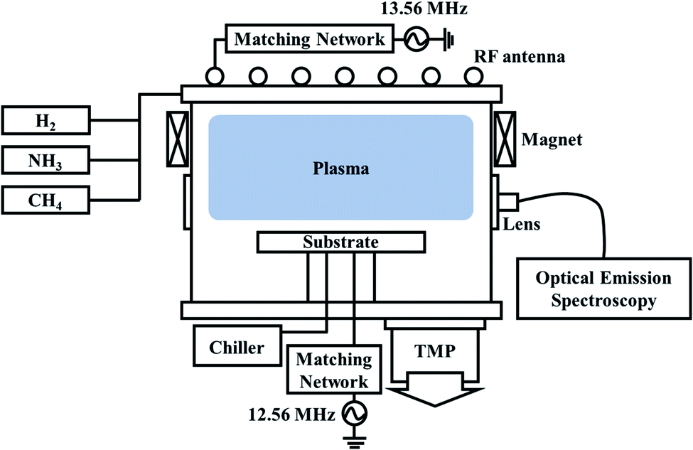 | ||
| Fig. 1 Schematic of the ICP etching system with hydrogen-based gases used for the etching of the OTS material. | ||
The cross section of the sample was observed via field emission scanning electron microscopy (FE-SEM, Hitachi S-4700) to measure the thickness of the etched OTS. Atomic force microscopy (AFM, Bruker Innova) was used to measure the root-mean-square (RMS) roughness of the OTS surface after the etching. The binding energies and surface composition of the OTS material before and after the etching were measured via X-ray photoelectron spectroscopy (XPS, ESCA 2000, VG Microtech Inc.) using a Mg Kα twin-anode source to observe the chemical damages in the OTS surface after etching using numerous gases. The XPS spectra were deconvoluted by the Avantage fitting program supplied by VG Microtech.
III. Results and discussion
Fig. 2(a) shows the etch rates of OTS materials for different gases such as H2, NH3, CH4, CH4 + H2 (1:1), and CH4 + NH3 (1:1) while keeping the other process conditions same. The ICP power, the bias power, and the operating pressures are maintained at 300 W, 50 W, and 5 mTorr, respectively. As shown in Fig. 2(a), OTS materials were etched by H2, CH4 + H2 (1:1), NH3, and CH4 + NH3 (1:1), while no etching of OTS materials was observed for CH4. In fact, a polymer based on hydrocarbon was deposited on the OTS surface when the OTS material was exposed to the CH4 plasma. For other plasmas formed with H2, CH4 + H2, NH3, and CH4 + NH3, the OTS etch rates were 0.28, 0.18, 0.52, and 0.45 nm s−1, respectively; therefore, the highest OTS etch rates were observed with NH3 plasma. Fig. 2(b) shows the etch selectivities of OTS over numerous materials such as TiN, Si3N4, and SiO2. No etch selectivity for the CH4 plasma was measured due to the deposition of a hydrocarbon polymer on OTS without etching. As shown in Fig. 2(b), in the case of TiN, the decreased etch selectivity in the order of NH3 (7.5), CH4 + NH3 (6.2), CH4 + H2 (0.9), and H2 (0.2) was observed. For Si3N4, the decreased etch selectivity in the order of CH4 + H2 (11), CH4 + NH3 (9.4), H2 (8.0), and NH3 (5.3), and for SiO2, the decreased etch selectivity in order of CH4 + NH3 (7.0), NH3 (3.2), CH4 + H2 (2.3), and H2 (1.4) were observed. Therefore, even though the highest etch selectivity of OTS was Si3N4 with CH4 + H2, the overall etch selectivities towards the materials investigated were the highest with CH4 + NH3.
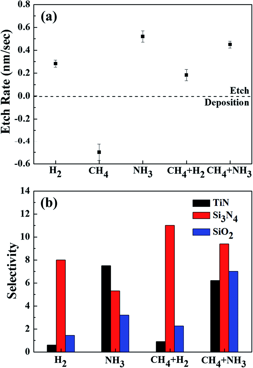 | ||
| Fig. 2 (a) Etch rates of the OTS material using H2, CH4, NH3, CH4 + H2 (1:1), and CH4 + NH3 (1:1). (b) Etch selectivities of OTS over TiN, Si3N4, and SiO2 for the etch conditions in (a). | ||
Table 1 shows the boiling points for the hydrides of OTS material components such as Ge, As, and Te. As shown in Table 1, the boiling points for the hydrides of Ge, As, Te were below 0 °C; therefore, those compounds can show high vapor pressures at room temperature. The etching of the OTS material using H2, CH4 + H2 (1:1), NH3, and CH4 + NH3 is related to the formation of volatile hydrogen compounds by the reaction of Ge, As, and Te in the OTS material with hydrogen atoms in the plasmas dissociated from the hydrogen containing gases. In the case of the CH4 plasma, even though hydrogen atoms dissociated from the CH4 plasma can also form volatile compounds with Ge, As, and Te in the OTS material due to the carbon remaining on the surface, instead of etching, a hydrocarbon polymer appeared to be deposited on the OTS material surface. By adding H2 to CH4, therefore, by using CH4 + H2 (1:1), the hydrocarbon polymer on the OTS material and OTS material itself were removed.
| Ge | As | Te | ||||
|---|---|---|---|---|---|---|
| Bonding | Bp (°C) | Bonding | Bp (°C) | Bonding | Bp (°C) | |
| a Bp: boiling point. | ||||||
| H | GeH4 | −88.5 | AsH3 | −62.5 | TeH2 | −2.2 |
| N | Ge3N4 | 900 | — | — | ||
The effect of hydrogen atoms on the OTS etching can be also understood for the etching using H2 and NH3 instead of CH4. The binding energies of H–H, C–H, and N–H are 436, 413, and 391 kJ mol−1, respectively; therefore, it is expected that more hydrogen atoms are dissociated for NH3 plasma than those for H2 and CH4 plasmas. The highest OTS etch rate with NH3 plasma among H2, CH4, and NH3 shown in Fig. 2 could be related to the highest hydrogen atom concentration in the plasma (the binding energies of the compounds formed by combining with the OTS material are as follows: the binding energies of Ge–H, As–H, Te–H, As–N, and Ge–C are 263.2, 274, 270.7, 489, and 455.7 kJ mol−1, respectively). Using OES, the amount of hydrogen atoms in the plasma was investigated, and the results are shown in Fig. 3(a). The process conditions are the same as those in Fig. 2; however, 5% Ar was added to the gases used in the OTS etching. As shown in Fig. 3(a), in the OES, emission peaks related to H atoms (Hβ and Hα) were identified at 486 and 656 nm in addition to Ar peaks at 751 and 763 nm. To estimate the relative hydrogen atom concentration dissociated in the plasma, that is, to remove the effect of the electron density on the OES peak intensity in measuring the concentration of dissociated species, the peak intensity ratio of H (656 nm)/Ar (751 nm) was taken, and the results are shown in Fig. 3(b). In fact, the excitation cross sections of H (656 nm) and Ar (751 nm) may not be similar, therefore, the ratio of H (656 nm)/Ar (751 nm) is only a rough estimation of hydrogen concentration. As shown in Fig. 3(b), the highest H (656 nm)/Ar (751 nm) was observed for NH3 among H2, CH4, NH3, CH4 + H2 (1:1), and CH4 + NH3 (1:1), indicating the possible highest OTS etch rate with NH3. The differences between the etch rates of hydrogen-based gases in Fig. 2 and the H peak intensity (H (656 nm)/Ar (751 nm)) of these gases in the plasma in Fig. 3(b) were CH4 and CH4 + H2 due to the formation of a hydrocarbon polymer on the OTS surface.
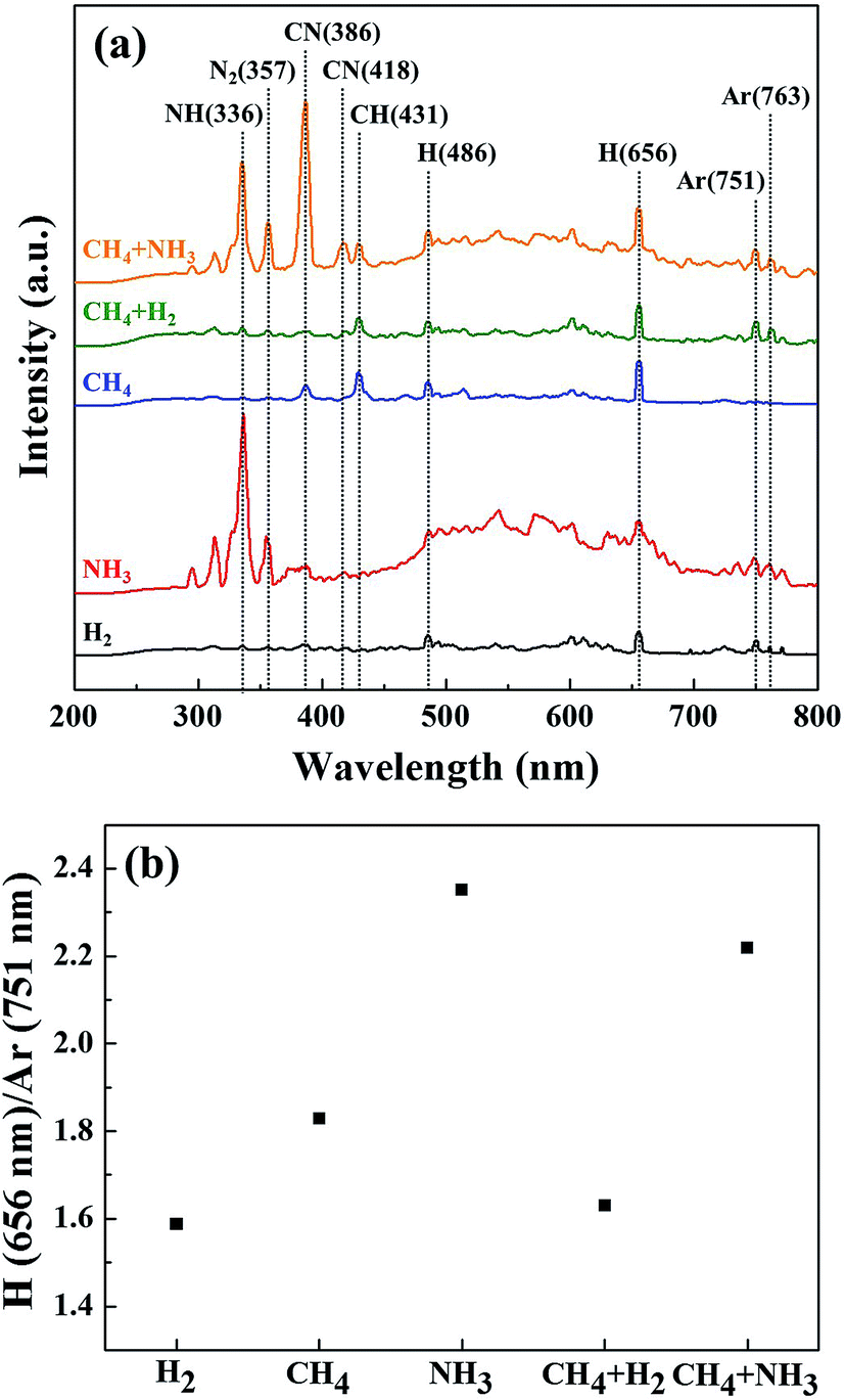 | ||
| Fig. 3 (a) OES spectra for H2, NH3, CH4 + H2 (1:1), and CH4 + NH3 (1:1). 5% Ar was added to the gases for the rough estimation of the hydrogen concentration in the plasma. (b) The peak intensity ratios of H (656 nm)/Ar (751 nm) for (a). | ||
After etching ∼20 nm of OTS (25 nm in thickness) using various hydrogen-based gases, the surface roughness of the remaining OTS material was measured using AFM, and the result is shown in Fig. 4(a) for RMS surface roughness values and Fig. 4(b) for 5 μm × 5 μm surface roughness images for Ar, H2, CH4 + H2, NH3, and CH4 + NH3. In the case of the OTS surface etched by CH4, due to no etching of OTS, no data was taken. To compare with pure sputtering, the OTS surface roughness etched using an Ar plasma (other conditions are the same as those in Fig. 3) was also included in Fig. 4. As shown in Fig. 4(a) and (b), in the case of the pure sputtering of the OTS material using the Ar plasma, the RMS surface roughness was ∼0.21 nm and was similar to that of OTS surface etched using H2 plasma (∼0.22 nm). The RMS surface roughness with CH4 + H2 (1:1) plasma (∼0.24 nm) was a little higher than that with Ar plasmas possibly due to the hydrocarbon polymer layer on the OTS surface. However, when the OTS material was etched using NH3 plasma, even though the etch rate was the highest among the gases investigated, as shown in Fig. 2, the OTS surface roughness was the highest as ∼0.35 nm. The increase in the surface roughness for the OTS material etched by NH3 plasma is believed to be related to the low vapor pressure of nitrogen compounds of an OTS component. As shown in Table 1, the boiling point of a Ge nitride such as Ge3N4 is 900 °C (the melting points/boiling points of the other component nitrides such as Te3−4N4 and AsN are not well known); therefore, the highest OTS surface roughness observed after the OTS etching using NH3 plasma is possibly related to the non-volatile nitride formation on the OTS surface during the etching.
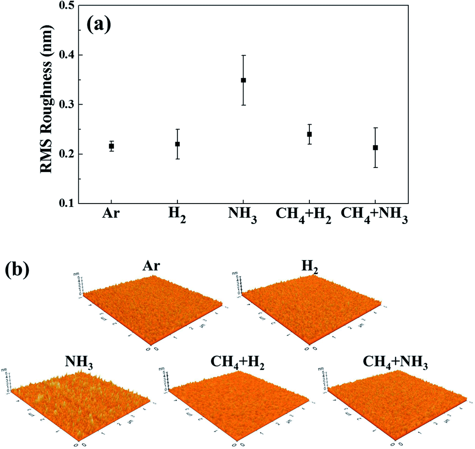 | ||
| Fig. 4 (a) Surface roughness measured by AFM after the partial etching (∼20 nm) of the 25 nm thick OTS material using Ar, H2, NH3, CH4 + H2, and CH4 + NH3 gases. (b) AFM images of etched OTS materials in 5 μm × 5 μm area. | ||
To remove (or not to form) the nitrides on the OTS surface during the etching using NH3, CH4 was added in the plasma; therefore, the OTS material was etched using the CH4 + NH3 (1:1) plasma. As shown in Fig. 2, the OTS etch rate using CH4 + NH3 was 0.45 nm s−1, which is a little lower than that using NH3 (0.52 nm s−1). However, as shown in Fig. 4, the surface roughness of OTS etched by CH4 + NH3 (1:1) (∼0.21 nm) was as low as that by Ar plasma. The high OTS etch rate and low OTS surface roughness etched by the CH4 + NH3 (1:1) plasma are believed to be related to the removal of nitrides on the OTS surface during the etching by the formation of volatile carbon nitrides (the boiling point of cyanogen, C2N2, is −21.1 °C and that of HCN is 25.6 °C) and to the decreased N flux from the plasma to the OST surface during the etching by the formation of CN in the plasma. As shown in Fig. 3(a), when the CH4 + NH3 (1:1) plasma was used instead of NH3, in addition to the OES peaks at 336 nm and 357 nm related to NH radical and N2 molecule, respectively, very high peak intensities related to CN at 386 nm and 418 nm were observed. This indicates the possibility of removing nitrides on the OTS surface formed by the etching using NH3 and the possibility of decreasing the N flux to the OTS surface during the etching.
The surface compositions of the OTS surfaces after etching using Ar, H2, NH3, CH4 + H2 (1:1), and CH4 + NH3 (1:1) plasmas were observed via XPS for the same etching conditions in Fig. 4, and the results are shown in Fig. 5. As shown in Fig. 5, the OTS surface composition after etching using Ar was Ge:As:Te:N:C = 20.7:62:16.1:0.3:0.9%, and after etching using H2, the surface composition was similar to that of Ar as Ge:As:Te:N:C = 22.3:58.2:17.9:0.5:1.1%, even though As was slightly decreased after etching using H2. However, after etching using NH3, the composition changed to Ge:As:Te:N:C = 14.1:49.4:14.7:21.4:0.4%, indicating a high nitrogen percentage on the OTS material surface by the etching using NH3. When the OTS was etched using CH4 + H2 (1:1), the OTS surface composition was Ge:As:Te:N:C = 9.73:52.07:5.58:0:32.62%, indicating a high carbon percentage on the OTS material surface. However, for the etching with CH4 + NH3 (1:1), not only significantly decreased surface nitrogen percentage but also significantly decreased carbon percentage (Ge:As:Te:N:C = 19.2:59.4:14.2:3.1:4.1%) could be observed on the etched OST surface.
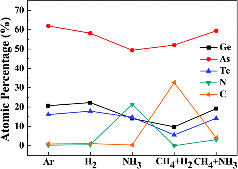 | ||
| Fig. 5 XPS surface composition of the OTS material etched by Ar, H2, NH3, CH4 + H2 (1:1), and CH4 + NH3 (1:1) gases. The OTS material was etched ∼20 nm. | ||
To investigate the formation of compounds such as nitrides and carbides formed on the etched OTS surfaces by the etching using NH3, CH4 + H2 (1:1), and CH4 + NH3 (1:1), the binding states of Ge, As, and Te on the etched OTS surfaces were investigated. Fig. 6(a)–(c) show the narrow scan XPS data of Ge, As, and Te, respectively, after the etching using Ar, H2, NH3, CH4 + H2 (1:1), and CH4 + NH3 (1:1) for the same etching conditions in Fig. 4. As shown in Fig. 6, after the etching using H2, the 3d peaks of Ge at 30.2 eV, 3d5/2/3d3/2 peaks of As at 40.9/42.4 eV, and 3d5/2/3d3/2 peaks of Te at 573.4/583.8 eV, which are similar to those of the OTS surface etched by the Ar plasma were observed, indicating no changes in the chemical binding states of the OTS material after the etching using H2. However, for the etching using NH3, for 3d Ge peak, an additional Ge peak at 31.8 eV, which is related to Ge–N is observed in Fig. 6(a). Similarly, as shown in Fig. 6(b) and (c), for the 3d5/2/3d3/2 peaks of As and Te, additional high binding energy peaks were observed at 41.6/43.8 eV and 575/585.2 eV, respectively, indicating the formation of As–N and Te–N, in addition to the Ge–N. Therefore, by the XPS analysis, the formation of nonvolatile nitrides of Ge, As, and Te on the etched OTS surface could be identified by the etching using NH3. For the OTS surface etched by CH4 + H2, for 3d Ge peak, an additional Ge peak at 32.6 eV, which is related to Ge–C was observed; however, no carbide peaks related to As and Te were observed possibly, indicating slight Ge–C formation of the OST surface in addition to the formation of a hydrocarbon polymer layer on the OTS surface. However, for CH4 + NH3, no nitrides or carbides of Ge, As, and Te could be observed on the OST material surface after the etching using CH4 + NH3 (1:1) possibly due to the formation of volatile C2N2, HCN, etc., by the reaction of CH4 + NH3 in the plasma and the reaction of N with the hydrocarbon on the materials surface, as shown in high CN-related peaks in Fig. 3.
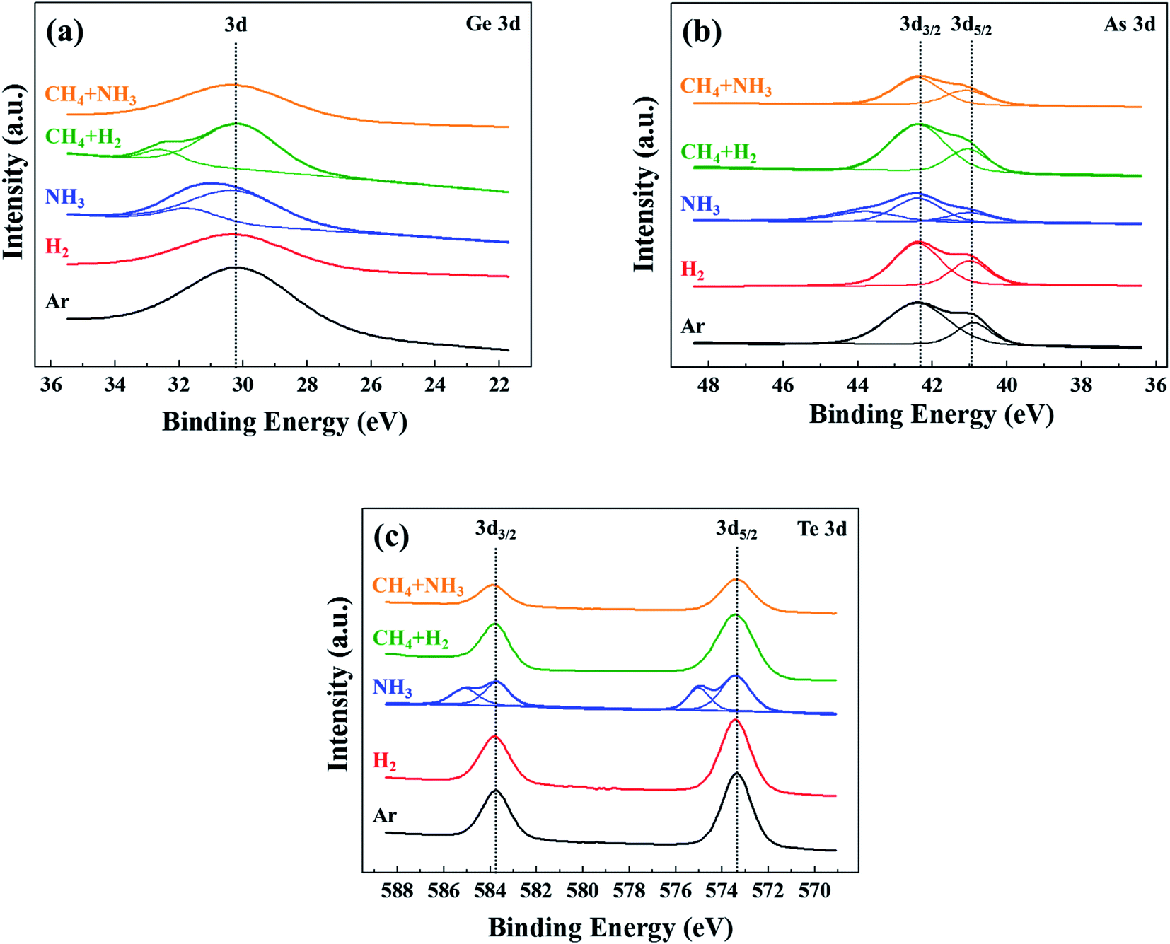 | ||
| Fig. 6 XPS narrow scan data of (a) Ge 3d, (b) As 3d, and (c) Te 3d on the OTS material surfaces etched by Ar, H2, NH3, CH4 + H2 (1:1), and CH4 + NH3 (1:1) gases. The OTS material was etched ∼20 nm. | ||
IV. Conclusions
In this study, the OTS material for PCRAM has been etched using reactive ion etching by hydrogen-based gases such as H2, CH4, CH4 + H2, NH3, and CH4 + NH3, and the etch characteristics by different hydrogen-based gases were investigated. Due to the high vapor pressures of the hydrides of Ge, As, and Te composing the OTS material, among the investigated gases, NH3 plasma exhibited the highest OTS material etch rate (0.52 nm s−1) possibly because of the highest dissociated hydrogen concentration in the plasma. In the case of CH4 plasma, even though hydrogen is dissociated from the CH4 plasma due to the carbon on the OTS surface, a polymer layer was deposited, and to etch the OTS material, the addition of H2 to CH4 was required. Even though NH3 plasma showed the highest OTS etch rate due to the nitride formation on the OTS surface, the high surface roughness was observed. By using CH4 + NH3 (1:1) instead of NH3, the OTS material could be etched at a high OTS etch rate (0.45 nm s−1) without the formation of nitrides and without increasing the surface roughness on the OTS material surface through the formation of volatile CN-related compounds.
Conflicts of interest
There are no conflicts to declare.Acknowledgements
This work is supported by the Samsung Electronics' university R&D program (development of post-etch passivation for prevent the oxidation in PRAM patterning) and the MOTIE (Ministry of Trade, Industry & Energy) (20003588) and KSRC (Korea Semiconductor Research Consortium) support program for the development of the future semiconductor device.References
- H.-S. P. Wong and S. Salahuddin, Nat. Nanotechnol., 2015, 10, 191–194 CrossRef CAS.
- R. Jeyasingh, J. Liang, M. A. Caldwell, D. Kuzum and H.-S. P. Wong, Proc. IEEE 2012 CICC, 2012 Search PubMed.
- A. Chen, Solid-State Electron., 2016, 125, 25–38 CrossRef CAS.
- S. Raoux, G. W. Burr, M. J. Breitwisch, C. T. Rettner, Y.-C. Chen, R. M. Shelby, M. Salinga, D. Krebs, S.-H. Chen, H.-L. Lung and C. H. Lam, IBM J. Res. Dev., 2008, 52, 465–479 CAS.
- A. V. Khvalkovskiy, D. Apalkov, S. Watts, R. Chepulskii, R. S. Beach, A. Ong, X. Tang, A. Driskill-Smith, W. H. Butler, P. B. Visscher, D. Lottis, E. Chen, V. Nikitin and M. Krounbi, J. Phys. D: Appl. Phys., 2013, 46, 139601 CrossRef.
- R. Waser, R. Dittmann, G. Staikov and K. Szot, Adv. Mater., 2019, 21, 2632–2663 CrossRef.
- R. Guo, L. You, Y. Zhou, Z. S. Lim, X. Zou, L. Chen, R. Ramesh and J. Wang, Nat. Commun., 2013, 4, 1990 CrossRef.
- W. Czubatyj and S. J. Hudgens, Electron. Mater. Lett., 2012, 8, 157–167 CrossRef CAS.
- G. W. Burr, M. J. Breitwisch, M. Franceschini, D. Garetto, K. Gopalakrishnan, B. Jackson, B. Kurdi, C. Lam, L. A. Lastras, A. Padilla, B. Rajendran, S. Raoux and R. S. Shenoy, J. Vac. Sci. Technol., B: Nanotechnol. Microelectron.: Mater., Process., Meas., Phenom., 2010, 28, 223–262 CAS.
- D. Loke, L. Shi, W. Wang, R. Zhao, H. Yang, L.-T. Ng, K.-G. Lim, T.-C. Chong and Y.-C. Yeo, Nanotechnol, 2011, 22, 254019 CrossRef.
- H.-S. P. Wong, S. Kim, J. Liang, J. P. Reifenberg, B. Rajendran, M. Asheghi and K. E. Goodson, Proc. IEEE, 2010, 98, 2201–2227 Search PubMed.
- K. L. Grosse, F. Xiong, S. Hong, W. P. King and E. Pop, Appl. Phys. Lett., 2013, 102, 193503 CrossRef.
- U. Russo, A. Redaelli and A. L. Lacaita, IEEE Trans. Electron. Dev., 2008, 55, 506–514 Search PubMed.
- Y. Koo, K. Baek and H. Hwang, 2016 Symp. on VLSI Tech. Dig., 2016 Search PubMed.
- G. Navarro, A. Verdy, N. Castellani, G. Bourgeois, V. Sousa, G. Molas, M. Bernard, C. Sabbione, P. Noe, J. Garrione, L. Fellouh and L. Perniola, 2017 Symp. on VLSI Tech. Dig., 2017 Search PubMed.
- H. Li and J. Robertson, Sci. Rep., 2019, 9, 1867 CrossRef.
- A. Velea, K. Opsomer, W. Devulder, J. Dumortier, J. Fan, C. Detavernier, M. Jurczak and B. Govoreanu, Sci. Rep., 2017, 7, 8103 CrossRef CAS.
- J. W. Park, D. S. Kim, W. O. Lee, J. E. Kim, H. Choi, O. Kwon, S. Chung and G. Y. Yeom, ECS J. Solid State Sci. Technol., 2019, 8, 341–345 CrossRef.
- G. Feng, B. Liu, Z. Song, S. Feng and B. Chen, Microelectron. Eng., 2008, 85, 1699–1704 CrossRef CAS.
- G. Feng, B. Liu, Z. Song, S. Feng and B. Chen, Electrochem. Solid-State Lett., 2007, 10, 47–50 CrossRef.
- N.-K. Min, A. Efremov, Y.-H. Kim, M. Kim, H.-H. Park, H. W. Lee and K.-H. Kwon, J. Vac. Sci. Technol., A, 2008, 26, 205–211 CrossRef CAS.
- Y. Song, R. Huang, Y. Zhang and H. Zhang, 2016 China Semicon. Technol. Int. Conf., 2016 Search PubMed.
- S.-K. Kang, M.-H. Jeon, J.-Y. Park, M. S. Jhon and G.-Y. Yeom, Jpn. J. Appl. Phys., 2011, 50, 086501 Search PubMed.
- J. Li, Y. Xia, B. Liu, G. Feng, Z. Song, D. Gao, Z. Xu, W. Wang, Y. Chan and S. Feng, Appl. Surf. Sci., 2016, 378, 163–166 CrossRef CAS.
- S. J. Pearton and F. Ren, J. Vac. Sci. Technol., B: Microelectron. Nanometer Struct.–Process., Meas., Phenom., 1993, 11, 15 CrossRef CAS.
| This journal is © The Royal Society of Chemistry 2020 |