
 Open Access Article
 This Open Access Article is licensed under a Creative Commons Attribution-Non Commercial 3.0 Unported Licence
The effects of stacking mode and thickness on the frictional behaviour of multilayer silicene
Chen Qian and
Jiugen Wang*
and
Jiugen Wang*
Department of Mechanical Engineering, Zhejiang University, 866 Yuhangtang Rd, Hangzhou 310058, P. R. China. E-mail: me_jg@zju.edu.cn; Tel: +86 13857146979
First published on 7th September 2020
Abstract
Understanding the contact behaviour of 2D materials in nanoscale is of great importance for their applications. In the present work, molecular dynamics simulation is employed to study the frictional behaviour of the AA′ and AB stacked multilayer silicene for up to 4 layers placed on the weakly adhesive amorphous SiO2 substrate with a sliding AFM tip. During the sliding process, the AFM cantilever represented by virtual atoms moves with the velocity of 2 m s−1 along the zigzag direction under a load of 2 nN at 300 K. The stick-slip frictional behaviour shows high sensitivity to the number of layers. As the thickness increases, the friction force first increases from the monolayer to bilayer and then decreases from the bilayer to 4-layer, which shows an exotic tendency for the first time among all the reported lamellar materials to date where the friction usually decreases monotonically with thickness. For all the investigated thicknesses, the friction on AA′-stacked silicene is slightly larger than the AB stacked counterpart, and the difference diminishes with increasing thickness. The frictional behaviour of AA′ bilayer presents the highest peak force with evolving weakening phenomenon induced by a phase transition to the planar structure. Herein, we analyze the frictional force distribution on the tip with kurtosis and skewness as measurement parameters for the commensurability and rigidity components, respectively. The contact area between silicene and the diamond tip is compared for different silicene morphologies. The result shows an affinity between friction and rigidity of multilayer silicene, which is closely related to the interlayer covalent bonds and limited shear between sublayers.
1. Introduction
With potential applications of 2D materials in Micro Electro Mechanical Systems (MEMS), it is important to investigate their behaviour upon contact with other materials. Considerable investigation has been made on graphene with the atomic force microscopy (AFM) in the past decade as it was the first nanomaterial prepared with thickness down to a single layer.1 Frictional experiments on graphene have reported reduced friction2 and have achieved superlubricity3–6 at low contact pressure. Solution-processed graphene drastically reduced the friction on the sliding steel surface with significant anti-corrosion properties.7 Graphene coating excellently improves the loading capacity of the substrate during nanoindentation and nano-scratching before rupture.8 Composite materials reinforced by graphene have reduced friction and wear with lubrication film.9 Moreover, the friction of graphene can be tuned and enhanced with fluorination.10 Graphene membranes on different substrate surfaces are expected to present different properties due to the integration of van der Waals forces or covalent bonds between graphene and the substrate.11 The stick-slip behaviour of graphene on weakly adhesive substrates shows the tendency of friction decreasing with the number of layers and the evolutional behaviour at the initial phase of the friction test was also observed for a thin-layered graphene.12 Molecular dynamics simulations were performed to elucidate the mechanism of local puckering around the contact area and the evolving commensurability between the AFM tip and graphene during the sliding process.13Silicene is a silicone analogue of graphene, featured with a low-buckled honeycomb structure due to the sp2 and sp3 hybridization. It has attracted significant attention due to its exotic properties as quantum dots14,15 and the affinity for ubiquitous silicon-based semiconductors.16 Silicene nanosheets were first epitaxially grown on Ag(111) via chemical vapour deposition17 and were later fabricated on Ag(110),18 Ir(111),19 ZrB2(0001),20 ZrC(111)21 and MoS2 (ref. 22) surfaces. The scalable preparation by liquid oxidation and exfoliation of CaSi2 was recently reported.23 It was predicted to have massless Dirac fermions as in graphene, while π and π* bands cross linearly at the K point of Brillouin zone.24 The bandgap can be opened with a vertical electrical field,25 making it a candidate for field-effect transistors.26 Oxidation,27 bilayer stacking mode,28,29 tensile strain30 and doping31 were also demonstrated for the tunable bandgap. Ab initio calculations and classical molecular dynamics simulation of monolayer silicene reported in-plane stiffness30 of 60.06 N m−1, 63.51 N m−1 and in-plane stress32 of 5.85 N m−1, 4.78 N m−1 in the zigzag and armchair directions, respectively, which are much lower as compared to graphene.33 The bending modulus of single-layer silicene is 0.44 eV, which is lowest among the known 2D materials.34 Unlike graphene, layers of multilayer silicene interact with strong covalent bonds instead of the weak van der Waals forces. As a result, the shearing motion between layers is confined for silicene. Above all, the frictional behaviour of silicene under AFM testing is expected to be different from graphene and merits further investigation.
Considering that the preparation technology of high-quality silicene with specific thickness and stacking mode remains to be developed, theoretical research has directive significance for the relationship between physical properties and the conformations of multilayers. Herein, molecular dynamics simulation (MD) is employed to study the frictional behaviour of silicene. The simulations show that the friction force during sliding is dependent on the number of layers and stacking mode. For most 2D materials that involve interlayer van der Waals forces like graphene and MoS2, friction monotonically decreases with the number of layers on weakly adhesive substrates. In contrast, friction on silicene firstly increases as the layer number changing from 1 to 2 and then decreases with larger thickness. The AA′ stacked multilayers exhibit higher friction than the AB stacked ones. Moreover, the abnormally large friction force of the AA′ bilayer is accompanied by an evolving decreasing phenomenon at the initial stage of the sliding process. The different friction forces on multilayers are compared and analyzed by the contact area and the distribution of friction force on the tip (more specifically, utilizing skewness and kurtosis) with circumspection. This work provides insight into the friction of multilayer silicene for the further exploration of such interlayer covalent bonded 2D materials.
2. Computational method
For a better description of the multilayer silicene conformation, two primary stacking modes are introduced. As elucidated in Fig. 1a, free-standing monolayer silicene presents a low-buckled honeycomb structure; its lattice parameters and buckled lengths are 3.84 Å and 0.404 Å, respectively. In Fig. 1b, the AA′ stacking mode consists of two adjacent layers with mirror symmetry, and the covalent bonds form between the upward silicon atoms of the first layer and the downward silicon atoms of the second layer. In Fig. 1c, the conformation of the AB stacking mode resembles that of graphite with displacement between two neighbouring layers but with covalent bonds between the upward atoms of the lower layer and downward atoms of the higher layer. Multilayer structures with the number of layers ranging from 1 to 4 in this article stack in either the AA′ or AB order. | ||
| Fig. 1 Top view (upper panel) and side view (lower panel) of the (3 × 3) supercell: (a) low buckled monolayer silicene (b) AA′ stacking mode (c) AB stacking mode. Silicon atoms in the first sublayer are represented with a larger radius than those in the second sublayer. Different colors denote atoms in different buckling directions of each sublayer. | ||
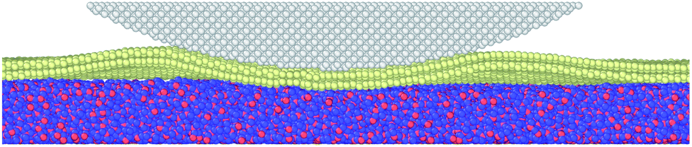
As illustrated in Fig. 2, the MD model geometry of the AFM test consists of an amorphous SiO2 substrate, silicene, and diamond tip apex. The size of the substrate is 400 Å × 400 Å × 15 Å with periodic boundary conditions in the x- and y-directions to mimic infinite size in a real experiment. Due to the chemically active surface of silicene, the amorphous SiO2 is chosen as the substrate to preserve the low-buckled structure of silicene. The amorphous SiO2 substrate has also been used for the modelling of heat dissipation in 2D transistors based on silicene.35 Silicene in contact with the diamond tip and placed on the SiO2 substrate was cut to the size of 380 Å × 380 Å. The x-direction and y-direction correspond to the zigzag and armchair directions of the silicene, respectively. The diamond tip apex is placed above the silicene with a radius of 163 Å and thickness of 20 Å. The hemispherical tip was adopted as it has been widely used in the MD frictional simulations on 2D materials.8,10,12,13,36,37 Besides, a hemispherical tip helps to avoid damage to the silicene as compared to a hard pyramidal AFM tip. Two virtual atoms are connected to the diamond tip with two springs. The lateral virtual atom coupled in the x-direction with a harmonic spring of 30 N m−1 moves with a constant velocity of 2 m s−1 and pulls the diamond tip forward during the friction test. The normal virtual atom coupled in the z-direction with a spring of 0.16 N m−1 is imposed with a constant load of 2 nN. The geometry of the tip and the stiffness of the harmonic springs in the lateral and normal directions are very close to the real experimental AFM tip and cantilever,12 as verified by the previous study.13 The MD simulation was performed with a Large-scale Atomic/Molecular Massively Parallel Simulator (LAMMPS)38 and was visualized using the Open Visualization Tool (OVITO)39 in this work.
 | ||
| Fig. 2 Illustration of the AFM friction model used in the molecular dynamics simulation. The diamond tip is coupled to two virtual atoms in the x- and z-directions with springs to mimic the AFM tip in experiments. The normal load is firstly imposed on the virtual atom in the z-direction and is transmitted to the tip. The virtual atom in the x-direction moves with constant velocity and pulls the tip forward during sliding. | ||
To obtain the amorphous SiO2 substrate, β-cristobalite of 406 Å × 406 Å × 43 Å was annealed at 6000 K and a pressure of 1 bar for 10 ps with a timestep of 0.1 fs and periodic boundary conditions,40 followed by rapid quenching to 300 K within 570 ps at a constant rate. After the temperature of SiO2 reached 300 K, the timestep was 0.5 fs from then on for higher computational efficiency. The bulk amorphous SiO2 was then cut in the z-direction to construct a free surface with enough vacuum space to eliminate periodic images. The energy was minimized using the conjugate gradient method, followed by relaxation for 200 ps under 300 K and 0 bar. The bottom 5 Å thickness of the SiO2 substrate was fixed after that. An isothermal-isobaric (NPT) ensemble with a Nose–Hoover thermostat and barostat was adopted for position and velocity updating during the preparation of the amorphous SiO2 substrate. Silicene with a size of 380 Å × 380 Å was then placed on the SiO2 surface, and the whole system was energy minimized and relaxed under 300 K for 100 ps. Marginal silicon atoms of the silicene sheet with a width of 10 Å were fixed to restrict the movement of the silicene on the substrate surface. We put the rigid diamond tip with a radius of 163 Å against the silicene. At the same time, two virtual atoms were coupled with the tip in the x- and z-direction, respectively, and the virtual atom in the normal direction was imposed with a load of 2 nN. Equilibrium was applied for 1 ns under 300 K after energy minimization for the whole system. After the equilibrium, we displaced the virtual atom in the x-direction (zigzag direction) with a speed of 2 m s−1 for 1.5 ns (3 nm sliding distance). We also restrained the displacement of the tip in the y-direction by a spring with an extremely large stiffness (1000 eV Å−2) tethered to the initially equilibrated y-position of the tip. It should be noted that the tip was treated as rigid for a better description of the subtle friction force distribution on the tip, which is crucial for the analysis of the friction force under different circumstances and will be discussed later. Besides, previous research showed no significant difference between the rigid and deformable tip sliding on graphene.13 During the friction process, the force on the lateral virtual atom was recorded as the friction force of the diamond tip, and the canonical ensemble (NVT) with the Nose–Hoover thermostat was employed for time integration.
The Tersoff potential parameterized by Munetoh for the Si–O system was used for the description of the interactions between Si–Si, Si–O, and O–O in the SiO2 substrate.41 This potential has successfully reproduced the pair distribution function, partial radial distribution function, bond angle distribution function and phonon density of state of SiO2 glass cooled from liquid SiO2 in good accordance with experimental data.42–44 To describe the interactions between the silicon atoms in the silicene sheet, the optimized Tersoff potential for silicene was used.45 The monolayer low-buckled free-standing silicene structure calculated with this potential has a lattice constant of 3.87 Å and buckling length of 0.655 Å, which is quite close to the structure optimized with DFT (b = 3.84 Å, Δ = 0.404 Å).34 The van der Waals force between the amorphous SiO2 substrate and silicene is modelled using Lennard-Jones (LJ) potential:
 | (1) |
3. Results and discussion
The friction force versus sliding distance curve is plotted in Fig. 4a. The typical stick-slip frictional behaviour of the AFM tip can be distinguished. The original data of the sliding process are plotted as dotted lines with noticeable oscillation. When the spring force is large enough to pull the tip forward, the tip moves with high velocity to the next potential barrier and the kinetic energy can be eased with thermal dissipation from the tip to silicene. Hence, the residual velocity gives rise to oscillation behaviour with the involvement of the lateral spring. To facilitate the observation of the friction data, the oscillation is then alleviated with smoothing by averaging every 25 ps, which is close to the vibration period in our simulation. From the smoothed data, it was observed that the friction force of monolayer silicene was relatively smaller as compared with the bilayer. The period of the friction force was about 3.88 Å in the sliding direction, which is almost equal to the lattice constant of the single-layer silicene. For bilayer silicene, the peak friction dramatically increased from 1.45 nN of the monolayer to 15.23 nN of the AA′ bilayer and 3.8 nN of the AB bilayer. In Fig. 4a, the peak force of the bilayer AA′ decreased during the sliding process, showing an evolving tendency. The period of the friction force is much larger than the lattice constant of the AA′ bilayer, indicating higher potential barriers for the movement of the diamond tip. The friction force for the AB bilayer is smaller than the AA′ with no evolution behaviour. For AA′ and AB 3-layer silicene, the peak force significantly decreased to 3.19 nN and 2.05 nN, respectively. Further decrease in the friction force was also observed for the case of the 4-layer: the first peak force was 2.06 nN for the AA′ 4-layer and 1.89 nN for the AB 4-layer. The period of the friction force was almost equal to the lattice constant for both 3-layer and 4-layer silicene. In all the simulations with the different number of layers, the AA′ stacked silicene multilayers showed greater friction force than the AB stacked ones, and the difference decreased with the increase in the thickness. The friction force circled in Fig. 4a for each morphology is plotted and compared in Fig. 4b.The frictional behaviour of multilayer silicene is quite different from the case of graphene or MoS2. The friction of multilayer graphene and MoS2 supported on weakly adhesive substrates usually decrease with an increasing number of layers monotonously. This difference is reasonable in consideration of the way the sublayers interact with each other. Sublayers of multilayer silicene are strongly covalently bonded to adjacent layers. Thus, the interlayer shear displacement between sublayers is confined. For graphene, the planar layers interact with each other through weak van der Waals forces, leading to an easy shear ability. Hence, it is more appropriate to consider multilayer silicene as a unit and multilayer graphene as several weakly connected individual layers. The in-plane stiffness and bending modulus of different stacked silicene morphologies are listed in Table 1. The multilayer silicene has in-plane stiffness that is almost 10% of the graphene counterpart, meaning that it is more susceptible to elastic deformation. The bending moduli of silicene are smaller than graphene for the single-layer and much more massive than the free ends graphene for multilayers. Besides, the bending modulus of silicene increases rapidly with thickness due to the strong covalent bonds between layers and the suppressed interlayer shear displacement. The shear deformation is crucial for the bending rigidity of multilayer 2D material. For graphene, the bending moduli obtained by MD simulations47,48 are significantly larger as compared to the self-folding experiment.49 The discrepancy can be ascribed to the different boundary conditions.49 For MD simulation, the edges of the bent graphene nanosheet are kept fixed, and the interlayer shear deformation is inhibited, whereas the free ends of multilayer graphene in the real bending experiment allow the interlayer shear deformation, leading to much lower bending moduli. For multilayer silicene, the interlayer covalent bonds are much stronger than the interlayer vdW forces of graphene. Thus the interlayer shear deformation is suppressed for multilayer silicene, even without constrained ends. With the participation of interlayer covalent bonds that impede the shear deformation between layers during the bending process, the bending modulus of multilayer silicene is expected to be more sensitive to the number of layers than graphene in the actual experiment.
| Morphology | In-plane stiffness (N m−1) | Bending modulus (eV) |
|---|---|---|
| Monolayer | 43.28/43.27 | 0.43688 |
| 2AA′ | 89.59/89.5 | 16.30044 |
| 2AB | 90.00/89.51 | 16.399 |
| 3AA′ | 134.96/135.58 | 50.61782 |
| 3AB | 134.32/135.29 | 50.99538 |
| 4AA′ | 180.48/180.63 | 80.99572 |
| 4AB | 179.76/179.73 | 78.28936 |
The silicene morphology under the tip features local corrugation around the contacted area, as illustrated in Fig. 3. The corrugation of lamellar 2D materials of different thicknesses causes different contact areas with the participation of van der Waals forces between the tip and 2D material. For multilayer graphene with weak interlayer interactions, the contact area decreases with thickness in a relatively mild way. In contrast, layers of multilayer silicene are covalently bonded, the bending rigidity of which remarkably increases with layer number. As a result, the contact area for silicene is supposed to decrease with increasing thickness with greater rapidity than graphene. In this article, we use the number of carbon atoms of the diamond tip in contact with the silicene sheet as a measurement for the contact area. A cutoff radius of 4 Å was used to define carbon and silicon atoms in touch. The contact area averaged over the sliding process versus the layer number is plotted in Fig. 5 for each stacking order. Not surprisingly, the number of carbon atoms in contact with silicene decreased dramatically with increasing thickness as expected. Among all the investigated multilayers, AA′ stacked silicene always shows a larger contact area than the AB stacked silicene at the same layer number. The contact area is partially attributed to the larger peak force of the AA′ stacked silicene in Fig. 4a. With the number of layers increasing from two to four, the decreasing contact area leads to the smaller friction force on multilayer silicene. However, it still cannot be explained why the friction force increases from monolayer to bilayer and why the frictional behaviour of the AA′ bilayer evolves during the sliding process.
 | ||
| Fig. 3 The corrugation morphology of the bilayer silicene in contact with the tip at the intersecting surface across the center of the tip. | ||
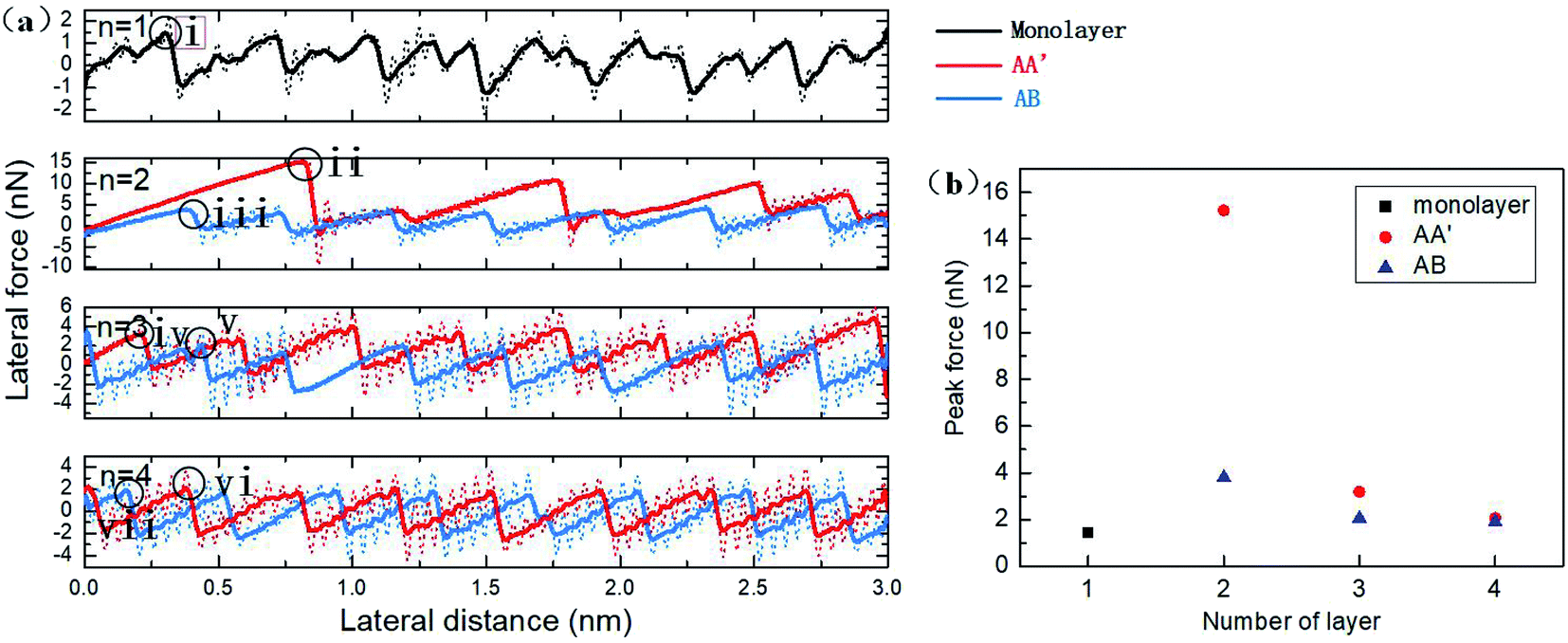 | ||
| Fig. 4 (a) Variation of the lateral force of the tip in the sliding process for AA′ and AB stacked silicene with the number of layers n = 1, 2, 3, 4. Original data are plotted as dotted lines and smoothed data as solid lines. Typical moments of maximum force are marked for each curve and will be analyzed later. (b) The peak force for monolayer, AA′ and AB stacked multilayer silicene with the different numbers of layers at the points marked in (a). | ||
 | ||
| Fig. 5 The average number of carbon atoms in contact with silicon atoms of multilayer silicene during the sliding process. The coordination number (CN), with a cutoff radius of 4 Å, was used to define the carbon atoms in contact with silicene. | ||
For further investigation, we analyzed the distribution of friction forces of the tip atoms in contact with silicene. Fig. 6 shows the distribution of force in the x-direction of the interface carbon atoms. Kurtosis and skewness are used to describe the friction force distribution of the interface tip atoms:
 | (2) |
 | (3) |
![[x with combining macron]](https://www.rsc.org/images/entities/i_char_0078_0304.gif) is the mean value of xi. Kurtosis is a measure of the flatness of the distribution data. Sharper kurtosis implies more leptokurtic and thick-tailed data. For example, the kurtosis of a normal distribution is 3. Kurtosis has been introduced in previous research regarding the strengthening friction at the initial stage of the sliding process for graphene.12 Kurtosis is interpreted as a measurement of the commensurability of the interface. Larger kurtosis indicates a more commensurable interface. In this article, we introduce skewness as a measurement of the component of friction related to the rigidity of multilayer silicene. Skewness is a reflection of the asymmetry of the probability distribution around its mean value. As the AFM tip slides across the silicene surface, the rigidity (especially bending stiffness) works as a resistance force ahead of the tip, leading to the asymmetric distribution of friction force on the interface. Therefore, a larger absolute value of skewness denotes a larger component of friction related to the rigidity of multilayer silicene. During the stick-slip process, the oscillation of the tip after a slip motion acts like noise to the frictional data. Nevertheless, the maximum friction force is less sensitive to the oscillation and more representative for analysis, since it is more related to the energy barrier for the tip. As the positive direction of force is the sliding direction, the skewness of force distribution is supposed to be a negative value. Fig. 7a shows the kurtosis value for the 7 moments marked in Fig. 4a, each one corresponds to the first peak force of each morphology. The kurtosis of monolayer and multilayer silicene ranges between 13.8 and 22.6, which is much larger than graphene (3.5–5.5 for single-layer graphene).13 The large kurtosis is a result of the small Young's modulus of silicene, which is almost 0.1 of graphene, making it more susceptible and commensurate on the interface. In Fig. 7a, the kurtosis values of the AA′ stacked silicenes are larger than the AB stacked ones for all the thicknesses, indicating the higher commensurability of the AA′ stacking mode. The AA′ bilayer has the highest kurtosis among the morphologies, which is consistent with the largest friction force of the AA′ bilayer. When we look into the overall trend of kurtosis, it is insufficient to explain the friction increment from the monolayer to the AA′ and AB bilayer. In Fig. 7b, we present the skewness of the marked moments from Fig. 4a. A dramatic increase in the absolute skewness value from the monolayer to AA′ and AB bilayer appeared with the magnitude increased by 11.3 and 5.3 times, respectively. For each layer number, the absolute value of skewness for stacked AA′ was larger than AB. The overall trend of skewness is wholly consistent with the friction force. As we look into the skewness of the AB 4-layer, it is unusual to find the skewness to be a positive value. Further simulation with the mass of the diamond tip decreased by a factor of ten was performed to eliminate excessive oscillation of the tip on the AB 4-layer, and the skewness at the first peak force was −0.0178742. The positive skewness value for the AB 4-layer seems to be a consequence of oscillation. It is worth noting that the functions of the contact area, commensurability and rigidity are not independent of each other. For example, the rigidity of the AB 4-layer is larger than the AB bilayer, but the contact area of the AB 4-layer is smaller than the AB bilayer; thus, the overall friction force on the AB 4-layer is smaller than the AB bilayer due to fewer components related to the rigidity (less absolute skewness value).
is the mean value of xi. Kurtosis is a measure of the flatness of the distribution data. Sharper kurtosis implies more leptokurtic and thick-tailed data. For example, the kurtosis of a normal distribution is 3. Kurtosis has been introduced in previous research regarding the strengthening friction at the initial stage of the sliding process for graphene.12 Kurtosis is interpreted as a measurement of the commensurability of the interface. Larger kurtosis indicates a more commensurable interface. In this article, we introduce skewness as a measurement of the component of friction related to the rigidity of multilayer silicene. Skewness is a reflection of the asymmetry of the probability distribution around its mean value. As the AFM tip slides across the silicene surface, the rigidity (especially bending stiffness) works as a resistance force ahead of the tip, leading to the asymmetric distribution of friction force on the interface. Therefore, a larger absolute value of skewness denotes a larger component of friction related to the rigidity of multilayer silicene. During the stick-slip process, the oscillation of the tip after a slip motion acts like noise to the frictional data. Nevertheless, the maximum friction force is less sensitive to the oscillation and more representative for analysis, since it is more related to the energy barrier for the tip. As the positive direction of force is the sliding direction, the skewness of force distribution is supposed to be a negative value. Fig. 7a shows the kurtosis value for the 7 moments marked in Fig. 4a, each one corresponds to the first peak force of each morphology. The kurtosis of monolayer and multilayer silicene ranges between 13.8 and 22.6, which is much larger than graphene (3.5–5.5 for single-layer graphene).13 The large kurtosis is a result of the small Young's modulus of silicene, which is almost 0.1 of graphene, making it more susceptible and commensurate on the interface. In Fig. 7a, the kurtosis values of the AA′ stacked silicenes are larger than the AB stacked ones for all the thicknesses, indicating the higher commensurability of the AA′ stacking mode. The AA′ bilayer has the highest kurtosis among the morphologies, which is consistent with the largest friction force of the AA′ bilayer. When we look into the overall trend of kurtosis, it is insufficient to explain the friction increment from the monolayer to the AA′ and AB bilayer. In Fig. 7b, we present the skewness of the marked moments from Fig. 4a. A dramatic increase in the absolute skewness value from the monolayer to AA′ and AB bilayer appeared with the magnitude increased by 11.3 and 5.3 times, respectively. For each layer number, the absolute value of skewness for stacked AA′ was larger than AB. The overall trend of skewness is wholly consistent with the friction force. As we look into the skewness of the AB 4-layer, it is unusual to find the skewness to be a positive value. Further simulation with the mass of the diamond tip decreased by a factor of ten was performed to eliminate excessive oscillation of the tip on the AB 4-layer, and the skewness at the first peak force was −0.0178742. The positive skewness value for the AB 4-layer seems to be a consequence of oscillation. It is worth noting that the functions of the contact area, commensurability and rigidity are not independent of each other. For example, the rigidity of the AB 4-layer is larger than the AB bilayer, but the contact area of the AB 4-layer is smaller than the AB bilayer; thus, the overall friction force on the AB 4-layer is smaller than the AB bilayer due to fewer components related to the rigidity (less absolute skewness value).
 | ||
| Fig. 6 Friction force distribution of tip atoms in contact with silicene at moments of maximum force marked in Fig. 4a. | ||
 | ||
| Fig. 7 Statistics of the friction force distribution of tip atoms in contact with multilayer silicene: (a) Kurtosis shows the commensurability between the diamond tip and silicene. Larger kurtosis corresponds to a more commensurate interface. (b) Skewness represents the measurement for the friction component related to the rigidity of silicene, which works as a resistance force from the corrugation in front of the sliding direction. The larger absolute value of the negative skewness shows the more crucial role of rigidity. Note that the abnormal small positive value of skewness for AB tetralayer silicene is proved to be a consequence of thermal oscillation by further simulation. | ||
The evolving weakening behaviour of friction force on the AA′ bilayer is strongly linked to the morphology around the corrugation. Fig. 8 shows the AA′ bilayer silicene coloured with the coordination number of silicon atoms with a cutoff radius of 3 Å at different stages of sliding. Perfect low-bucked AA′ bilayer silicene has coordination numbers of 50% of 3, and 50% of 4. Meanwhile, the planar bilayer silicene is only characterized by a coordination number of 4. The AA′ bilayer silicene underneath the diamond tip transits to the planar structure under compression at the start of sliding in Fig. 8a. The lattice constant of the planar bilayer is 4.09 Å and is larger than 3.83 Å of the AA′ bilayer. Consequently, the phase transition gives rise to the larger contact area of the AA′ bilayer in Fig. 4a, while the major part of silicene in contact is still the low-bucked AA′ stacked bilayer. During the sliding process, a more planar bilayer structure appears and merges in the contact area in Fig. 8b–d. The energy barrier of the planar structure for tip movement is less than the AA′ bilayer due to the smooth surface of the planar structure. The role of the reduced energy barrier on the planar structure is critical since the percentage in the contact area increases with the sliding process and induces the evolving weakening frictional behaviour. The phase transition from the AA′ bilayer to the planar structure also occurs during tension according to the previous report.50
 | ||
| Fig. 8 Coordination numbers (CN) of silicon atoms of AA′ bilayer silicene at different moments of the sliding process, with sliding distances equal to (a) 0; (b) 10 Å; (c) 20 Å; (d) 30 Å. Contact areas are circled with blue lines and the bilayer planar phase with black lines. | ||
For comparison, multilayer 2D materials (e.g. graphene, MoS2, h-BN) involving weak interlayer van der Waals forces can easily shear and only allow the topmost layers to be lifted for corrugation. Consequently, the frictional behaviour of such multilayer materials is mainly governed by the interaction between the tip and the topmost layer13 and the role of rigidity as a function of thickness is negligible. In contrast, silicene layers are strongly coupled through the covalent bonds, interlayer shear is inhibited, and the topmost layer cannot be lifted separately. Therefore, the role of rigidity should be taken into account when discussing the relationship between friction and the number of layers for the interlayer covalently bonded 2D materials like silicene.
4. Conclusion
In this work, we present the frictional behaviour of multilayer silicene as a function of stacking order and number of layers. The load of 2 nN, sliding path along the zigzag direction and velocity of 2 m s−1 at 300 K were considered The result is more complicated than graphene with the participation of the strong covalent bond between the silicene layers. For thickness between 2 and 4 layers, AA′ stacked silicenes show larger friction forces than the AB stacked silicenes as a consequence of the contact area. The friction increases from monolayer to bilayer and decreases as the thickness increases from 2 to 4 layers for both stacking orders. The friction force distribution of contact silicon atoms was analyzed to explain the frictional behaviour during the sliding process. We introduced skewness as a measurement for the friction component related to the rigidity of the silicene. The bilayer with the largest skewness reached to the maximum value of friction force as a compromise between rigidity and contact area for each stacking order. Although the stiffness of the AA′ and AB 3-layer and 4-layer silicene is larger than their bilayer counterparts, the small contact area leads to a smaller friction component related to the rigidity (skewness) and their lower friction. The AA′ bilayer showed the highest friction force and also an evolving weakening trend with sliding distance as a result of the phase transition from the low-buckled AA′ bilayer to the planar bilayer structure.Conflicts of interest
There are no conflicts to declare.Acknowledgements
We are grateful to the National Supercomputer Center in Guangzhou for high-performance computational resource.References
- K. S. Novoselov, A. K. Geim, S. V. Morozov, D. Jiang, Y. Zhang, S. V. Dubonos, I. V. Grigorieva and A. A. Firsov, Science, 2004, 306, 666–669 CrossRef CAS
.
- T. Filleter, J. L. McChesney, A. Bostwick, E. Rotenberg, K. V. Emtsev, T. Seyller, K. Horn and R. Bennewitz, Phys. Rev. Lett., 2009, 102, 086102 CrossRef CAS
- X. Feng, S. Kwon, J. Y. Park and M. Salmeron, ACS Nano, 2013, 7, 1718–1724 CrossRef CAS
- D. Berman, S. A. Deshmukh, S. K. R. S. Sankaranarayanan, A. Erdemir and A. V. Sumant, Science, 2015, 348, 1118–1122 CrossRef CAS
- S. Kawai, A. Benassi, E. Gnecco, H. Soede, R. Pawlak, X. Feng, K. Muellen, D. Passerone, C. A. Pignedoli, P. Ruffieux, R. Fasel and E. Meyer, Science, 2016, 351, 957–961 CrossRef CAS
- S.-W. Liu, H.-P. Wang, Q. Xu, T.-B. Ma, G. Yu, C. Zhang, D. Geng, Z. Yu, S. Zhang, W. Wang, Y.-Z. Hu, H. Wang and J. Luo, Nat. Commun., 2017, 8, 14029 CrossRef CAS
- D. Berman, A. Erdemir and A. V. Sumant, Carbon, 2013, 54, 454–459 CrossRef CAS
- A. Klemenz, L. Pastewka, S. G. Balakrishna, A. Caron, R. Bennewitz and M. Moseler, Nano Lett., 2014, 14, 7145–7152 CrossRef CAS
- A. D. Moghadam, E. Omrani, P. L. Menezes and P. K. Rohatgi, Composites, Part B, 2015, 77, 402–420 CrossRef
- Q. Li, X. Z. Liu, S. P. Kim, V. B. Shenoy, P. E. Sheehan, J. T. Robinson and R. W. Carpick, Nano Lett., 2014, 14, 5212–5217 CrossRef CAS
- G. Zhao, X. Li, M. Huang, Z. Zhen, Y. Zhong, Q. Chen, X. Zhao, Y. He, R. Hu, T. Yang, R. Zhang, C. Li, J. Kong, J.-B. Xu, R. S. Ruoff and H. Zhu, Chem. Soc. Rev., 2017, 46, 4417–4449 RSC
- C. Lee, Q. Li, W. Kalb, X.-Z. Liu, H. Berger, R. W. Carpick and J. Hone, Science, 2010, 328, 76–80 CrossRef CAS
- S. Li, Q. Li, R. W. Carpick, P. Gumbsch, X. Z. Liu, X. Ding, J. Sun and J. Li, Nature, 2016, 539, 541–545 CrossRef CAS
- L. B. Drissi, H. Ouarrad, F. Z. Ramadan and W. Fritzsche, RSC Adv., 2020, 10, 801–811 RSC
- B.-R. Wu, RSC Adv., 2019, 9, 32782–32790 RSC
- D. D. de Vargas and R. J. Baierle, RSC Adv., 2020, 10, 8927–8935 RSC
- B. Lalmi, H. Oughaddou, H. Enriquez, A. Kara, S. Vizzini, B. Ealet and B. Aufray, Appl. Phys. Lett., 2010, 97, 223109 CrossRef
- B. Aufray, A. Kara, S. Vizzini, H. Oughaddou, C. Léandri, B. Ealet and G. Le Lay, Appl. Phys. Lett., 2010, 96, 183102 CrossRef
- L. Meng, Y. Wang, L. Zhang, S. Du, R. Wu, L. Li, Y. Zhang, G. Li, H. Zhou, W. A. Hofer and H.-J. Gao, Nano Lett., 2013, 13, 685–690 CrossRef CAS
- A. Fleurence, R. Friedlein, T. Ozaki, H. Kawai, Y. Wang and Y. Yamada-Takamura, Phys. Rev. Lett., 2012, 108, 245501 CrossRef
- T. Aizawa, S. Suehara and S. Otani, J. Phys. Chem. C, 2014, 118, 23049–23057 CrossRef CAS
- D. Chiappe, E. Scalise, E. Cinquanta, C. Grazianetti, B. van den Broek, M. Fanciulli, M. Houssa and A. Molle, Adv. Mater., 2014, 26, 2096–2101 CrossRef CAS
- J. Liu, Y. Yang, P. Lyu, P. Nachtigall and Y. Xu, Adv. Mater., 2018, 30, 1800838 CrossRef
- S. Cahangirov, M. Topsakal, E. Aktürk, H. Şahin and S. Ciraci, Phys. Rev. Lett., 2009, 102, 236804 CrossRef CAS
- Z. Ni, Q. Liu, K. Tang, J. Zheng, J. Zhou, R. Qin, Z. Gao, D. Yu and J. Lu, Nano Lett., 2012, 12, 113–118 CrossRef CAS
- L. Tao, E. Cinquanta, D. Chiappe, C. Grazianetti, M. Fanciulli, M. Dubey, A. Molle and D. Akinwande, Nat. Nanotechnol., 2015, 10, 227–231 CrossRef CAS
- Y. Du, J. Zhuang, H. Liu, X. Xu, S. Eilers, K. Wu, P. Cheng, J. Zhao, X. Pi and K. W. See, ACS Nano, 2014, 8, 10019–10025 CrossRef CAS
- J. E. Padilha and R. B. Pontes, J. Phys. Chem. C, 2015, 119, 3818–3825 CrossRef CAS
- H. Fu, J. Zhang, Z. Ding, H. Li and S. Meng, Appl. Phys. Lett., 2014, 104, 131904 CrossRef
- H. Zhao, Phys. Lett. A, 2012, 376, 3546–3550 CrossRef CAS
- Z. Ni, H. Zhong, X. Jiang, R. Quhe, G. Luo, Y. Wang, M. Ye, J. Yang, J. Shi and J. Lu, Nanoscale, 2014, 6, 7609–7618 RSC
- R. E. Roman and S. W. Cranford, Comput. Mater. Sci., 2014, 82, 50–55 CrossRef CAS
- Y. Y. Zhang and Y. T. Gu, Comput. Mater. Sci., 2013, 71, 197–200 CrossRef CAS
- C. Qian and Z. Li, Comput. Mater. Sci., 2020, 172, 109354 CrossRef
- H. Zhang, H. Wang, S. Xiong, H. Han, S. Volz and Y. Ni, J. Phys. Chem. C, 2018, 122, 2641–2647 CrossRef CAS
- L. Bai, B. Liu, N. Srikanth, Y. Tian and K. Zhou, Nanotechnology, 2017, 28, 355704 CrossRef
- J. Sarkar and D. Das, Comput. Mater. Sci., 2018, 147, 64–71 CrossRef CAS
- S. Plimpton, J. Comput. Phys., 1995, 117, 1–19 CrossRef CAS
- A. Stukowski, Modell. Simul. Mater. Sci. Eng., 2010, 18, 015012 CrossRef
- Z.-Y. Ong and E. Pop, Phys. Rev. B: Condens. Matter Mater. Phys., 2010, 81, 155408 CrossRef
- S. Munetoh, T. Motooka, K. Moriguchi and A. Shintani, Comput. Mater. Sci., 2007, 39, 334–339 CrossRef CAS
- J. Sarnthein, A. Pasquarello and R. Car, Phys. Rev. B: Condens. Matter Mater. Phys., 1995, 52, 12690 CrossRef CAS
- P. A. V. Johnson, A. C. Wright and R. N. Sinclair, J. Non-Cryst. Solids, 1983, 58, 109–130 CrossRef CAS
- J. M. Carpenter and D. L. Price, Phys. Rev. Lett., 1985, 54, 441–443 CrossRef CAS
- G. P. P. Pun and Y. Mishin, Phys. Rev. B: Condens. Matter Mater. Phys., 2017, 95, 224103 CrossRef
- J.-Y. Chung, V. Sorkin, Q.-X. Pei, C.-H. Chiu and Y.-W. Zhang, J. Phys. D: Appl. Phys., 2017, 50, 345302 CrossRef
- D. Sen, K. S. Novoselov, P. M. Reis and M. J. Buehler, Small, 2010, 6, 1108–1116 CrossRef CAS
- S. Cranford and M. J. Buehler, Modell. Simul. Mater. Sci. Eng., 2011, 19, 054003 CrossRef
- X. Chen, C. Yi and C. Ke, Appl. Phys. Lett., 2015, 106, 101907 CrossRef
- Y. He, H. Li, F. Wei, J. Qi, Q. Meng and Y. Sui, Comput. Mater. Sci., 2017, 134, 153–159 CrossRef CAS
| This journal is © The Royal Society of Chemistry 2020 |