
 Open Access Article
 This Open Access Article is licensed under a
 Creative Commons Attribution 3.0 Unported Licence
Controlling the oxidation state of molybdenum oxide nanoparticles prepared by ionic liquid/metal sputtering to enhance plasmon-induced charge separation†
Kazutaka Akiyoshia,
Tatsuya Kameyama a,
Takahisa Yamamotoa,
Susumu Kuwabatab,
Tetsu Tatsumac and
Tsukasa Torimoto*a
a,
Takahisa Yamamotoa,
Susumu Kuwabatab,
Tetsu Tatsumac and
Tsukasa Torimoto*a
aGraduate School of Engineering, Nagoya University, Furo-cho, Chikusa-ku, Nagoya 464-8603, Japan. E-mail: torimoto@apchem.nagoya-u.ac.jp
bGraduate School of Engineering, Osaka University, 2-1 Yamada-oka, Suita, Osaka 565-0871, Japan
cInstitute of Industrial Science, The University of Tokyo, 4-6-1 Komaba, Meguro-ku, Tokyo 153-8505, Japan
First published on 3rd August 2020
Abstract
Nanoparticles composed of molybdenum oxide, MoOx, were successfully prepared by room-temperature ionic liquid (RTIL)/metal sputtering followed by heat treatment. Hydroxyl groups in RTIL molecules retarded the coalescence between MoOx NPs during heat treatment at 473 K in air, while the oxidation state of Mo species in MoOx nanoparticles (NPs) could be modified by changing the heat treatment time. An LSPR peak was observed at 840 nm in the near-IR region for MoOx NPs of 55 nm or larger in size that were annealed in a hydroxyl-functionalized RTIL. Photoexcitation of the LSPR peak of MoOx NPs induced electron transfer from NPs to ITO electrodes.
Introduction
Light irradiation of plasmonic nanoparticles (NPs) can induce a collective oscillation of free carriers, so-called localized surface plasmon resonance (LSPR), that can lead to the generation of strong electromagnetic fields at the surfaces.1 When plasmonic NPs were combined with a semiconductor such as TiO2 or ZnO, plasmon-induced charge separation (PICS),2–5 by which electrons or holes moved from the NPs to the semiconductor, was observed. Recently, there have been some reports published on PICS from plasmonic NPs to metallic conductors such as graphene substrates6–9 and indium tin oxide (ITO) electrodes.10–15 This phenomenon has been intensively investigated for the development of photovoltaics, photocatalysts, and biosensors.2–5,16–18 So far, most research on PICS has been carried out with metal NPs showing intense LSPR peaks, such as Au and Ag.Recently, much attention has been given to the development of novel plasmonic nanostructures with less expensive materials. Among the various materials for possible application, metal oxides have been promising because the position of LSPR peaks was reported to be easily controlled over a wide wavelength region from visible light to near-IR light by changing the composition.19–21 For example, several kinds of semiconductor/metal oxide systems including TiO2/MoO3,22 TiO2/ITO,23 and SnO2/ITO24 have been reported to exhibit PICS. However, the preparation methods have not yet been completely optimized. Furthermore, the efficiency of PICS has been low at a longer wavelength because the energy of absorbed photons seemed to be too low for photogenerated electrons to overcome the Schottky barrier height at the metal–semiconductor interface.4,25–29
On the other hand, room-temperature ionic liquids (RTILs) have been fascinating media to prepare nanostructured materials because the obtained structures were quite stable without the addition of any stabilizing agents.30–39 We have reported strategies to prepare metal and alloy NPs by sputtering a metal onto RTILs under a reduced pressure, the RTIL/metal sputtering technique, with the use of unique features of RTILs such as extremely low vapor pressure and high thermal stability.40–42 This technique enabled clean preparation of plasmonic NPs such as Au,43 Ag,44 Cu,45 AgAu,46 and AuCu.47 Furthermore, when transition metals with relatively negative redox potentials were sputter-deposited on RTILs, corresponding metal oxides, such as indium oxide,48 molybdenum oxide, and tungsten oxide,49 were formed via oxidation with O2 or H2O contained in the RTIL as an impurity. However, the optical properties of thus-obtained NPs have not been reported.
In this study, we controlled the oxidation state of molybdenum oxide NPs prepared by the RTIL/metal sputtering technique and we investigated their LSPR properties. Furthermore, their PICS behaviour was clarified by irradiating thus-obtained NPs immobilized on ITO electrodes.
Experimental
Preparation of molybdenum oxide NPs
RTILs of 1-hydroxyethyl-3-methylimidazolium tetrafluoroborate (HyEMI-BF4) and 1-ethyl-3-methylimidazolium tetrafluoroborate (EMI-BF4) were dried at 373 K for 3 h with vigorous stirring under a vacuum condition before use. The contents of water were determined to be 560 ppm and 90 ppm for HyEMI-BF4 and EMI-BF4, respectively, by the Karl Fischer titration method (Kyoto Electronics Manufacturing, MKC-610). An RTIL (0.60 cm3) was spread on a glass plate (10 cm2) that was horizontally set in the sputter coater (Sanyu Electron Co. Ltd., SC-701HMCII). The surface of the RTIL was located at a distance of 25 mm from the Mo target (99.99% in purity). Sputter deposition of Mo on RTILs was carried out for 1 h with a discharge current of 10, 20, 30, or 40 mA under argon pressure of 3.0 Pa. The as-sputter-deposited NPs were further oxidized to produce MoOx NPs by annealing RTILs containing NPs at 473 K for various times, typically 30 min, in air with relative humidity of 40–50%.Extinction spectra of NPs in RTILs were measured by a spectrophotometer (Agilent Technologies, Agilent 8453) in which a quartz cell with a light path length of 0.10 mm was used, and a blank solution for the measurements was an RTIL without metal sputtering. The concentration of Mo deposited in an RTIL was determined by X-ray fluorescence spectroscopy (Rigaku, EDXL300). Structural morphology of the NPs was observed by using a transmission electron microscope (TEM; HITACHI, H-7650) operated with an acceleration voltage at 100 kV. A Cs-corrected HR-STEM (JEOL, ARM-200F) with an acceleration voltage of 200 kV was used to acquire high-resolution TEM images. Samples for TEM observation were prepared by dipping a copper grid with amorphous carbon overlayers (Oken Shoji, # 10-1012) into the RTIL containing NPs. The excess amount of RTIL was rinsed with acetonitrile followed by drying. X-ray diffraction (XRD) patterns were measured with an X-ray diffractometer (Rigaku, SmartLab-3K) using Cu Kα radiation. The samples for the XRD measurements were prepared by separating the NPs from RTILs. A large amount of acetonitrile was added to NP-containing RTILs. The resulting mixture was centrifuged, and the precipitates were set onto a low-background silicon sample holder.
Photoelectrochemical measurements
MoOx NPs were isolated by centrifugation at 15![[thin space (1/6-em)]](https://www.rsc.org/images/entities/char_2009.gif) 000 rpm for 5 min and washed with acetonitrile several times. The thus-obtained NPs were finally dispersed in acetonitrile. The MoOx NP dispersion was spread on an ITO substrate, followed by drying. The resulting electrode with NPs of 9.4 × 10⁻⁶ mol cm−2 as Mo atoms was used as a working electrode for photoelectrochemical measurements, and an Ag/AgCl electrode and a Pt wire were used as a reference electrode and a counter electrode, respectively. The MoOx NP-immobilized ITO electrodes, ITO/MoOx NPs, were irradiated with a Xe lamp (λ > 350 nm) in a 0.5 mol dm−3 Na2SO4 aqueous solution (pH 6.5), the light intensity of which was 0.37 W cm−2. Action spectra of the photocurrent were obtained by passing the light of the Xe lamp through a monochromator (Jasco, CT-10), in which the incident photon-to-electron conversion efficiency (IPCE) was plotted as a function of the wavelength of irradiated monochromatic light.
000 rpm for 5 min and washed with acetonitrile several times. The thus-obtained NPs were finally dispersed in acetonitrile. The MoOx NP dispersion was spread on an ITO substrate, followed by drying. The resulting electrode with NPs of 9.4 × 10⁻⁶ mol cm−2 as Mo atoms was used as a working electrode for photoelectrochemical measurements, and an Ag/AgCl electrode and a Pt wire were used as a reference electrode and a counter electrode, respectively. The MoOx NP-immobilized ITO electrodes, ITO/MoOx NPs, were irradiated with a Xe lamp (λ > 350 nm) in a 0.5 mol dm−3 Na2SO4 aqueous solution (pH 6.5), the light intensity of which was 0.37 W cm−2. Action spectra of the photocurrent were obtained by passing the light of the Xe lamp through a monochromator (Jasco, CT-10), in which the incident photon-to-electron conversion efficiency (IPCE) was plotted as a function of the wavelength of irradiated monochromatic light.
Results and discussion
Preparation of molybdenum oxide NPs showing LSPR
We previously reported that sputter deposition of Mo on EMI-BF4 produced NPs composed of molybdenum oxide with various Mo valences.49 However, their optical properties were not clarified. Thus, at first, we investigated the influence of the kind of RTILs used on the optical properties of deposited NPs.The colour of the Mo-deposited HyEMI-BF4 solution was remarkably changed by heat treatment from yellow brown at 0 min, dark brown at 30 min, to light brown at 120 min. As shown in Fig. 1a, the NPs in HyEMI-BF4 solution exhibited a structureless spectrum just after Mo sputter deposition, but the following heat treatment at 473 K resulted in the development of a new peak at ca. 840 nm. The peak intensity increased with the elapse of heating time to 30 min and then decreased with further heating. Since the LSPR peak of chemically synthesized oxygen-deficient MoO3 NPs was reported to be located in the wavelength range of 600–1000 nm,50–53 the observed peak at ca. 840 nm was assignable to the LSPR peak of molybdenum oxide NPs. Furthermore, heating of NPs in HyEMI-BF4 also increased the extinction at a wavelength of 700 nm or shorter.
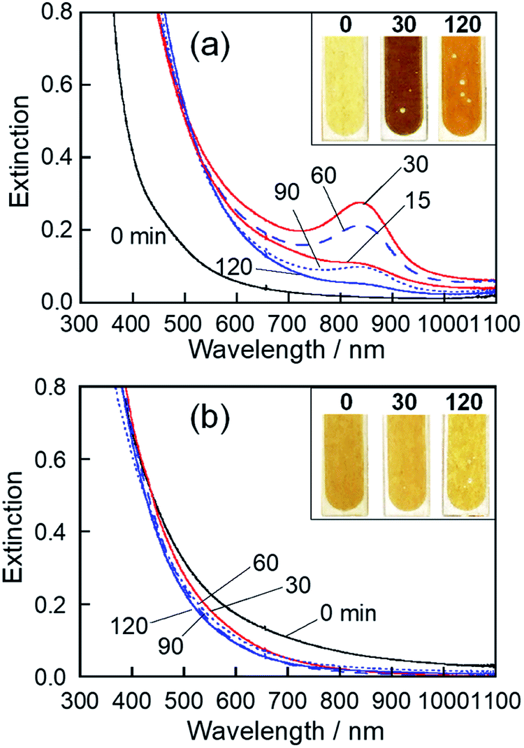 | ||
| Fig. 1 Extinction spectra of NPs in HyEMI-BF4 (a) and EMI-BF4 (b) prepared by Mo sputtering (discharge current of 30 mA) and their changes with heating at 473 K for various times in air. Photographs of the solutions with heating times of 0, 30, and 120 min are shown in the insets of the corresponding panels. | ||
O 1s XPS spectra (Fig. S1†) revealed the presence of Mo–O2−, Mo–O− and Mo–OH species as well as adsorbed H2O on the surface (Mo–H2O) in deposited NPs, regardless of the heat treatment. Fig. 2 shows the Mo 3d XPS spectra of NPs deposited in HyEMI-BF4 with different heating times. The obtained signals were successfully deconvoluted with Mo 3d5/2 and 3d3/2 of 230.8 eV and 234.1 eV for Mo(IV), 231.5 eV and 234.6 eV for Mo(V), and 232.7 and 235.8 eV for Mo(VI), respectively.54 We could obtain fractions of Mo species with different oxidation states from XPS signals, as shown in Table S1.† The fraction of Mo(VI) was increased from 25.7% to 68.3% in the total Mo species with heat treatment from 0 to 120 min. No signals assignable to those at 228.3 and 231.5 eV for 3d5/2 and 3d3/2, respectively, of Mo(0)54 were detected. These results indicated that the metallic Mo species deposited were immediately oxidized by oxygen molecules in air and/or H2O molecules contained in the RTIL as an impurity and then NPs of molybdenum oxides, MoOx, were formed in HyEMI-BF4. Furthermore, we estimated the compositions of thus-obtained MoOx NPs heat-treated for 0, 30 and 120 min to be x = 1.69, 2.29, and 3.09, respectively, from XPS signals of Mo and O.
 | ||
| Fig. 2 XPS spectra for Mo 3d levels of as-deposited MoOx NPs in HyEMI-BF4 (a) and those after annealing at 473 K for 30 (b) and 120 min (c). The Mo sputtering was carried out with a discharge current of 30 mA. | ||
The colour of EMI-BF4 sputter-deposited with Mo was slightly changed from brown to yellow-brown by heat treatment. Fig. 1b shows extinction spectra of as-deposited MoOx NPs in EMI-BF4 and those heat-treated in air at 473 K for various times. A structureless spectrum was observed for as-deposited NPs in EMI-BF4, being similar to those in HyEMI-BF4. Heating Mo-deposited EMI-BF4 for 30 min slightly induced a blueshift of extinction spectra to the onset wavelength around 800 nm without showing an LSPR peak at around 800–900 nm, and further heat treatment up to 120 min scarcely changed the extinction spectra. XPS spectra of MoOx NPs deposited in EMI-BF4 (Fig. S2†) revealed that MoOx NPs were composed of Mo(IV), Mo(V), and Mo(VI) species, in which the fraction of Mo(VI) was roughly constant at ca. 20–27% regardless of the heating (Table S1†), being different from the case of the NPs in HyEMI-BF4. The compositions of MoOx NPs deposited in EMI-BF4 were also determined from XPS signals to be x = 1.17, 1.61 and 2.60 for samples heat-treated for 0, 30 and 120 min, respectively. It should be noted that each x value for MoOx NPs in EMI-BF4 was smaller than the aforementioned value of corresponding NPs in HyEMI-BF4, indicating the NPs in EMI-BF4 are less susceptible to oxidation.
As already reported in the literature, NPs consisting of metal oxide semiconductors with an oxygen-deficient composition, such as WO3−y and MoO3−y, can absorb light through three different electronic excitation modes: (i) interband transition, that is, transition from the valence band (VB) to the conduction band (CB), (ii) transition from the VB to oxygen-deficient states formed by metal species of different valences, such as Mo(V), and (iii) polaron-induced LSPR.55–58 In such metal oxide semiconductors, it was reported that the optical response was extended to a longer wavelength range than that expected from the intrinsic energy gap,59 because oxygen vacancies formed defect states between the CB and the Fermi level (EF), narrowing their optical band gap. Considering the MoO3 energy gap of approximately 3 eV, corresponding to 413 nm,55,60 the extinction in the wavelength region of 700 nm or shorter in Fig. 1 seemed to be due to transition from the VB to oxygen vacancy states formed by Mo(IV) and Mo(V) species.
The appearance of the LSPR peak of MoOx NPs in HyEMI-BF4 can be understood by considering two factors, the amount of oxygen vacancies and particle size. As mentioned above for the results shown in Fig. 2 and Table S1,† heat treatment of MoOx NPs deposited in HyEMI-BF4 remarkably increased the fraction of Mo(VI) in the total Mo species with the elapse of heating time. When NPs in HyEMI-BF4 were heated for 30 min at 473 K, the Mo(IV) species disappeared. For such NPs, the chemical formula was calculated to be MoO2.29, the amount of oxygen vacancies of which was smaller than that of as-sputter-deposited NPs in EMI-BF4, MoO1.61. These results suggested that an appropriate amount of oxygen vacancies was formed with heat treatment for 30 min and could then produce free electrons in the MoO3 structure for the LSPR peak shown in Fig. 1a to emerge. However, the LSPR peak almost disappeared with further heat treatment, and the chemical formula of NPs changed from MoO2.29 to MoO3.09 with prolonged heating from 30 to 120 min (Table S1†). The decrease in the amount of oxygen vacancies resulted in a reduction in the number of free electrons.61,62 Another reason for the decrease in LSPR peak intensity was the change in size of MoOx NPs with heating. It is well known that the position of LSPR peaks is very sensitive to the size of plasmonic nanoparticles, regardless of metals or metal oxides, being red-shifted with an increase in particle size.63,64
Fig. 3 shows TEM images of MoOx NPs deposited in HyEMI-BF4 and EMI-BF4. As-deposited NPs in HyEMI-BF4 were spherical particles with sizes of 6.8 ± 4.9 nm, which were larger than those formed in EMI-BF4, 2.2 ± 1.0 nm. Heating at 473 K caused significant coalescence between NPs. After heating for 30 min, the NPs in HyEMI-BF4 were ca. 65 nm in size, being much smaller than those in EMI-BF4, ca. 200 nm or more. It was reported previously that thermal oxidation of In metal in EMI-BF4 at 523 K produced largely aggregated NPs but that similar heat treatment in HyEMI-BF4 gave uniformly dispersed In2O3 NPs of 28 nm in diameter, indicating that hydroxyl groups in cationic species of RTILs were strongly adsorbed on the metal oxide surface to improve the dispersibility of NPs in the solutions.65 Thus, the results of the present study suggested that hydroxyl groups in HyEMI-BF4 molecules could be adsorbed on the MoOx surface to retard the coalescence between NPs. The concentration of water in RTILs was also reported to significantly affect the size of In2O3 NPs formed, and the larger NPs were produced with an increase in the water concentration in RTILs.65 In the present study, since the water concentration in HyEMI-BF4, 590 ppm, was much larger than that in EMI-BF4, 90 ppm, a higher growth rate of MoOx was expected in HyEMI-BF4, resulting in a larger number of NPs with a smaller average size. In both kinds of RTIL, the heated NPs were connected with each other to form a network structure. Furthermore, prolonged heat treatment for 120 min remarkably enlarged the size of NPs to several micrometres. Thus, it was thought that the formation of larger MoOx NPs, >200 nm, in EMI-BF4 prevented the appearance of the LSPR peak.
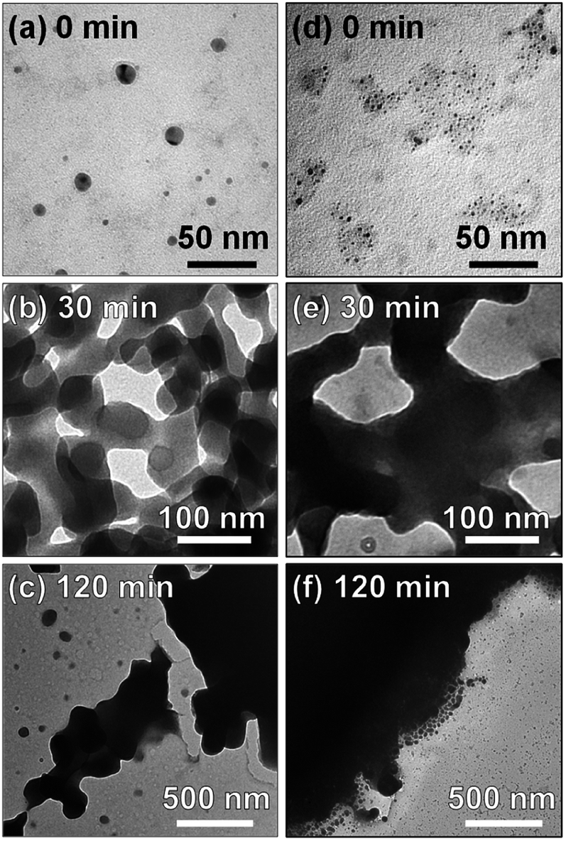 | ||
| Fig. 3 TEM images of as-deposited MoOx NPs (a and d) and those after annealing at 473 K for 30 (b and e) and 120 min (c and f). The RTILs used were HyEMI-BF4 (a–c) and EMI-BF4 (d–f). The Mo sputtering was carried out with a discharge current of 30 mA. | ||
Fig. 4 shows high-resolution TEM images of MoOx NPs formed in HyEMI-BF4. Lattice fringes with interplanar spacings of 0.26 and 0.33 nm were observed for as-deposited NPs in HyEMI-BF4 and those heat-treated at 473 K for 30 min, being assignable to (111) and (021) planes of orthorhombic MoO3 crystal structure, respectively. As shown in Fig. 4a, most as-deposited NPs showed lattice fringes only in a partial area of the particle. On the other hand, large particles obtained after annealing were composed of small NPs of ca. 1.5–6 nm in size as shown in Fig. 4b and many grain boundaries could be recognized inside the particle, indicating that each particle was polycrystalline. It should be noted that as-sputter-deposited NPs showed no characteristic diffraction peaks in the XRD patterns (Fig. S3†), though the NPs after heating at 473 K for 30 min exhibited a broad diffraction peak at ca. 24–27°, being assignable to orthorhombic MoO3 structure. These results suggested that the as-deposited NPs were composed of amorphous phase containing a very small amount of orthorhombic MoO3 crystal phase that could not be detected by XRD analysis but that the heat treatment increased both the fraction of orthorhombic crystal phase in NPs and their crystallinity as well as the size of coalesced NPs.
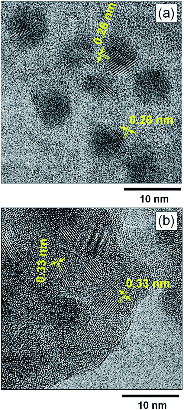 | ||
| Fig. 4 High-resolution TEM images of (a) as-deposited MoOx NPs in HyEMI-BF4 and (b) those after annealing at 473 K for 30 min. | ||
The discharge current used for the RTIL/metal sputtering technique is an important parameter for controlling the concentrations of metal species sputter-deposited in RTILs. For example, the concentrations of Au and Ag NPs deposited, as well as the size of NPs deposited, were increased with an increase in the discharge current.66,67 We investigated the influence of discharge current on the LSPR peak of the resulting MoOx NPs. As-deposited NPs in HyEMI-BF4 exhibited a larger extinction at a wavelength shorter than 800 nm in individual spectra but did not show any LSPR peaks (Fig. S4†). The extinction at a constant wavelength was enlarged with an increase in the discharge current. The size of as-sputter-deposited MoOx NPs increased from 2.0 nm to 17 nm with an increase in the discharge current from 10 mA to 40 mA (not shown). The concentration of Mo atoms deposited in HyEMI-BF4 linearly increased with increase in the discharge current (inset of Fig. 5b). On the other hand, the LSPR peak appeared at ca. 840 nm as shown in Fig. 5a when the NPs sputter-deposited with a discharge current of 20 mA or larger were heat-treated at 473 K for 30 min in air. Heating as-deposited NPs enlarged the particle size, accompanied by interconnection between the resulting NPs to form a network structure (Fig. S5†). Fig. 5b shows the size of heat-treated MoOx NPs as a function of discharge current. With an increase in the discharge current from 10 mA to 40 mA, the average size of resulting NPs increased from 32 nm to 131 nm, indicating that the degree of coalescence increased with an increase in the Mo concentration in the solution. As clearly shown in Fig. 5b, an LSPR peak appeared at 840 nm for MoOx NPs with sizes of 55 nm or larger. It was reported that spherical Au NPs smaller than ca. 2 nm did not show a clear LSPR peak.68–70 Thus, the results suggest that the minimum size for showing an LSPR peak is ca. 55 nm for MoOx NPs prepared in the present study.
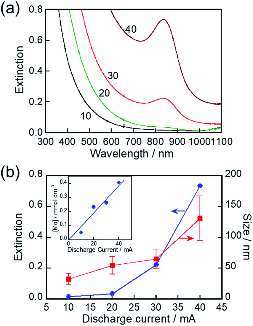 | ||
| Fig. 5 (a) Extinction spectra of NPs sputter-deposited in HyEMI-BF4 with various discharge currents after heating at 473 K for 30 min. Discharge currents in units of mA are shown in the panel. (b) Plots of extinction at 840 nm in panel a and size of heat-treated MoOx NPs in the solution as a function of discharge current (inset). Relationship between concentration of Mo atoms sputter-deposited in HyEMI-BF4 and discharge current. | ||
Plasmon-induced charge transfer from MoOx NPs
As mentioned above, we successfully prepared MoOx NPs with or without showing an LSPR peak in the near-IR region by changing the kind of RTIL used for sputter deposition. These NPs seem to be suitable for investigating the photoelectrochemical response of MoOx NPs with LSPR excitation in the near-IR wavelength region. Fig. 6a shows photocurrent–potential curves of ITO/MoOx NPs, where MoOx NPs were prepared by Mo sputter deposition in HyEMI-BF4 and EMI-BF4 followed by heat treatment at 473 K for 30 min in air. Anodic photocurrents were observed at a more positive potential than −0.1 V vs. Ag/AgCl in both cases, the magnitude being increased with a positive shift of the applied potential. These results indicated that the obtained MoOx NPs exhibited a photoresponse similar to that of an n-type semiconductor photoelectrode, as reported previously.55,71 Furthermore, it should be noted that the NPs prepared in EMI-BF4 exhibited a much lower photoactivity than that of NPs prepared in HyEMI-BF4, suggesting the presence of a larger amount of carrier recombination sites or trap sites in NPs.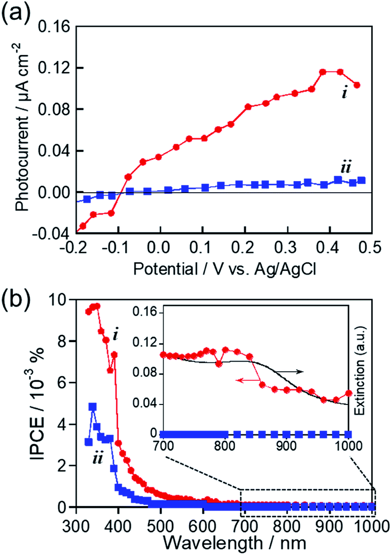 | ||
| Fig. 6 (a) Photocurrent–potential curves for ITO/MoOx NP electrodes. The MoOx NPs were prepared by Mo sputter deposition in HyEMI-BF4 (i) and EMI-BF4 (ii) with a discharge current of 30 mA followed by heat treatment at 473 K for 30 min in air. (b) Action spectra of anodic photocurrents in panel a under potential application at 0.5 V vs. Ag/AgCl. | ||
Photocurrent action spectra were measured under potential application at 0.5 V vs. Ag/AgCl. As shown in Fig. 6b, photoexcitation of the interband transition of MoO3 with light of wavelengths shorter than ca. 400 nm produced a predominant fraction of anodic photocurrent in both cases, though the NPs prepared in HyEMI-BF4 exhibited higher IPCE values than those of NPs prepared in EMI-BF4. No photocurrent in the near-IR region was observed for NPs in EMI-BF4. However, the peak assignable to LSPR of MoOx NPs at around 840 nm was observed in the action spectrum for NPs prepared in HyEMI-BF4, and the spectrum outline agreed well with that of their extinction spectrum. This suggested that PICS was observed for ITO/MoOx NPs: the LSPR excitation produced electrons excited in the conduction band of MoOx NPs, which were injected into the ITO electrode.15 It should be noted that the IPCEs obtained with excitation of the LSPR peak of MoOx NPs were considerably lower than those with photoexcitation of the interband transition at ca. 400 nm or shorter. It was reported that PICS systems with photoexcitation of near-IR light, such as ITO/TiO2/ITO NPs23 and ITO/Au NPs/TiO2,29 exhibited relatively low IPCEs of similar order of magnitude to those shown in Fig. 6b. The low IPCEs obtained in the near-IR region were probably because the energy of excited electrons, generated by LSPR photoexcitation, was too low to overcome the Schottky barrier height at the metal–semiconductor interface and/or because back-electron transfer easily occurred from conducting electrodes to plasmonic NPs. Thus, we concluded that the RTIL/metal sputtering technique provides a useful strategy for preparing plasmonic MoOx NPs and that LSPR excitation enables plasmon-induced charge transfer from thus-obtained NPs to ITO electrodes.
Conclusions
We successfully prepared MoOx NPs showing an LSPR peak in the near-IR region by RTIL/metal sputtering followed by heat treatment. The degree of coalescence between NPs was dependent on the kind of RTIL used, and hydroxyl groups in RTIL molecules could be adsorbed on the MoOx surface to stabilize NPs in the RTIL. Heat treatment of as-deposited MoOx NPs enabled control of the oxidation state of Mo species in NPs. The LSPR peak was observed in the near-IR region for MoOx NPs of 55 nm or larger in size that were prepared in a hydroxyl-functionalized RTIL. Photoexcitation of the LSPR peak of MoOx NPs induced electron transfer from NPs to ITO electrodes. The photoresponsivity of MoOx in the near-IR region will be useful for developing novel plasmonic devices such as photocatalysts and solar cells.72 Our RTIL/metal sputtering technique coupled with heat treatment will provide a useful strategy for controlling the oxidation states of metal oxide particles for plasmonic nanostructures.Conflicts of interest
There are no conflicts to declare.Acknowledgements
This work was financially supported by JSPS KAKENHI grant numbers JP16H06507 in Scientific Research on Innovative Areas “Nano-Material Optical-Manipulation,” JP18H03927, and JP18K19128.References
- H. Raether, Surface Plasmons on Smooth and Rough Surfaces and on Gratings, Springer-Verlag, Berlin, 1988 Search PubMed.
- Y. Tian and T. Tatsuma, J. Am. Chem. Soc., 2005, 127, 7632 CrossRef CAS PubMed.
- C. Clavero, Nat. Photonics, 2014, 8, 95 CrossRef CAS.
- M. L. Brongersma, N. J. Halas and P. Nordlander, Nat. Nanotechnol., 2015, 10, 25 CrossRef CAS PubMed.
- T. Tatsuma, H. Nishi and T. Ishida, Chem. Sci., 2017, 8, 3325 RSC.
- D. Kumar, A. Lee, T. Lee, M. Lim and D.-K. Lim, Nano Lett., 2016, 16, 1760 CrossRef CAS PubMed.
- W. Lin, Y. Cao, P. Wang and M. Sun, Langmuir, 2017, 33, 12102 CrossRef CAS PubMed.
- E. Cao, X. Guo, L. Zhang, Y. Shi, W. Lin, X. Liu, Y. Fang, L. Zhou, Y. Sun, Y. Song, W. Liang and M. Sun, Adv. Mater. Interfaces, 2017, 4, 1700869 CrossRef.
- W. Lin, E. Cao, L. Zhang, X. Xu, Y. Song, W. Liang and M. Sun, Nanoscale, 2018, 10, 5482 RSC.
- L. B. Lowe, S. H. Brewer, S. Krämer, R. R. Fuierer, G. Qian, C. O. Agbasi-Porter, S. Moses, S. Franzen and D. L. Feldheim, J. Am. Chem. Soc., 2003, 125, 14258 CrossRef CAS PubMed.
- K. Kawahara, K. Suzuki, Y. Ohko and T. Tatsuma, Phys. Chem. Chem. Phys., 2005, 7, 3851 RSC.
- A. Al-Zubeidi, B. S. Hoener, S. S. E. Collins, W. Wang, S. R. Kirchner, S. A. H. Jebeli, A. Joplin, W.-S. Chang, S. Link and C. F. Landes, Nano Lett., 2019, 19, 1301 CrossRef PubMed.
- E. Pensa, J. Gargiulo, A. Lauri, S. Schlücker, E. Cortés and S. A. Maier, Nano Lett., 2019, 19, 1867 CrossRef CAS PubMed.
- H. Nishi and T. Tatsuma, Nanoscale, 2019, 11, 19455 RSC.
- T. Tatsuma and H. Nishi, Nanoscale Horiz., 2020, 5, 597 RSC.
- A. Furube and S. Hashimoto, NPG Asia Mater., 2017, 9, e454 CrossRef CAS.
- K. Ueno, T. Oshikiri, Q. Sun, X. Shi and H. Misawa, Chem. Rev., 2018, 118, 2955 CrossRef CAS PubMed.
- N. Wu, Nanoscale, 2018, 10, 2679 RSC.
- J. M. Luther, P. K. Jain, T. Ewers and A. P. Alivisatos, Nat. Mater., 2011, 10, 361 CrossRef CAS PubMed.
- S. D. Lounis, E. L. Runnerstrom, A. Llordés and D. J. Milliron, J. Phys. Chem. Lett., 2014, 5, 1564 CrossRef CAS PubMed.
- A. Agrawal, S. H. Cho, O. Zandi, S. Ghosh, R. W. Johns and D. J. Milliron, Chem. Rev., 2018, 118, 3121 CrossRef CAS PubMed.
- S. H. Lee, H. Nishi and T. Tatsuma, Nanoscale, 2018, 10, 2841 RSC.
- S. H. Lee, H. Nishi and T. Tatsuma, Phys. Chem. Chem. Phys., 2019, 21, 5674 RSC.
- M. Sakamoto, T. Kawawaki, M. Kimura, T. Yoshinaga, J. J. M. Vequizo, H. Matsunaga, C. S. K. Ranasinghe, A. Yamakata, H. Matsuzaki, A. Furube and T. Teranishi, Nat. Commun., 2019, 10, 406 CrossRef PubMed.
- Y. Nishijima, K. Ueno, Y. Kotake, K. Murakoshi, H. Inoue and H. Misawa, J. Phys. Chem. Lett., 2012, 3, 1248 CrossRef CAS PubMed.
- A. O. Govorov, H. Zhang and Y. K. Gun'ko, J. Phys. Chem. C, 2013, 117, 16616 CrossRef CAS.
- C. Ng, J. J. Cadusch, S. Dligatch, A. Roberts, T. J. Davis, P. Mulvaney and D. E. Gomez, ACS Nano, 2016, 10, 4704 CrossRef CAS PubMed.
- H. Nishi and T. Tatsuma, J. Phys. Chem. C, 2018, 122, 2330 CrossRef CAS.
- K. Akiyoshi and T. Tatsuma, Photochem. Photobiol. Sci., 2019, 18, 1727 RSC.
- E. F. Borra, O. Seddiki, R. Angel, D. Eisenstein, P. Hickson, K. R. Seddon and S. P. Worden, Nature, 2007, 447, 979 CrossRef CAS PubMed.
- J. Dupont and J. D. Scholten, Chem. Soc. Rev., 2010, 39, 1780 RSC.
- H. Wender, P. Migowski, A. F. Feil, S. R. Teixeira and J. Dupont, Coord. Chem. Rev., 2013, 257, 2468 CrossRef CAS.
- M. Armand, F. Endres, D. R. MacFarlane, H. Ohno and B. Scrosati, Nat. Mater., 2009, 8, 621 CrossRef CAS PubMed.
- S. Wegner and C. Janiak, Top. Curr. Chem., 2017, 375, 65 CrossRef PubMed.
- Y. Hatakeyama, S. Takahashi and K. Nishikawa, J. Phys. Chem. C, 2010, 114, 11098 CrossRef CAS.
- Z. He and P. Alexandridis, Phys. Chem. Chem. Phys., 2015, 17, 18238 RSC.
- H. Konnerth and M. H. G. Prechtl, Green Chem., 2017, 19, 2762–2767 RSC.
- C. Verma, E. E. Ebenso and M. A. Quraishi, J. Mol. Liq., 2019, 276, 826 CrossRef CAS.
- M. Meischein, M. Fork and A. Ludwig, Nanomaterials, 2020, 10, 525 CrossRef CAS PubMed.
- T. Torimoto, K. Okazaki, T. Kiyama, K. Hirahara, N. Tanaka and S. Kuwabata, Appl. Phys. Lett., 2006, 89, 243117 CrossRef.
- T. Torimoto, T. Tsuda, K. Okazaki and S. Kuwabata, Adv. Mater., 2010, 22, 1196 CrossRef CAS PubMed.
- S. Kuwabata, T. Tsuda and T. Torimoto, J. Phys. Chem. Lett., 2010, 1, 3177 CrossRef CAS.
- E. Vanecht, K. Binnemans, J. W. Seo, L. Stappers and J. Fransaer, Phys. Chem. Chem. Phys., 2011, 13, 13565 RSC.
- S. C. Hamm, R. Shankaran, V. Korampally, S. Bok, S. Praharaj, G. A. Baker, J. D. Robertson, B. D. Lee, S. Sengupta, K. Gangopadhyay and S. Gangopadhyay, ACS Appl. Mater. Interfaces, 2012, 4, 178 CrossRef CAS PubMed.
- K. Richter, A. Birkner and A.-V. Mudring, Angew. Chem., Int. Ed., 2010, 49, 2431 CrossRef CAS PubMed.
- K. Okazaki, T. Kiyama, K. Hirahara, N. Tanaka, S. Kuwabata and T. Torimoto, Chem. Commun., 2008, 691 RSC.
- D. König, K. Richter, A. Siegel, A.-V. Mudring and A. Ludwig, Adv. Funct. Mater., 2014, 24, 2049 CrossRef.
- T. Suzuki, K. Okazaki, S. Suzuki, T. Shibayama, S. Kuwabata and T. Torimoto, Chem. Mater., 2010, 22, 5209 CrossRef CAS.
- T. Suzuki, S. Suzuki, Y. Tomita, K. Okazaki, T. Shibayama, S. Kuwabata and T. Torimoto, Chem. Lett., 2010, 39, 1072 CrossRef CAS.
- H. Cheng, T. Kamegawa, K. Mori and H. Yamashita, Angew. Chem., Int. Ed., 2014, 53, 2910 CrossRef CAS PubMed.
- J. Shi, Y. Kuwahara, M. Wen, M. Navlani-Garcia, K. Mori, T. An and H. Yamashita, Chem.–Asian J., 2016, 11, 2377 CrossRef CAS PubMed.
- X. Tan, L. Wang, C. Cheng, X. Yan, B. Shen and J. Zhang, Chem. Commun., 2016, 52, 2893 RSC.
- S. H. Lee, H. Nishi and T. Tatsuma, Chem. Commun., 2017, 53, 12680 RSC.
- Z. Song, T. Cai, Z. Chang, G. Liu, J. A. Rodriguez and J. Hrbek, J. Am. Chem. Soc., 2003, 125, 8059 CrossRef CAS PubMed.
- I. A. de Castro, R. S. Datta, J. Z. Ou, A. Castellanos-Gomez, S. Sriram, T. Daeneke and K. Kalantar-zadeh, Adv. Mater., 2017, 29, 1701619 CrossRef PubMed.
- Z. Hai, Z. Wei, C. Xue, H. Xud and F. Verpoort, J. Mater. Chem. C, 2019, 7, 12968 RSC.
- S. S. Kalanur, I.-H. Yoo, I.-S. Cho and H. Seo, Electrochim. Acta, 2019, 296, 517 CrossRef CAS.
- H. Quan, Y. Gao and W. Wang, Inorg. Chem. Front., 2020, 7, 817 RSC.
- Y. Wang, J. Cai, M. Wu, J. Chen, W. Zhao, Y. Tian, T. Ding, J. Zhang, Z. Jiang and X. Li, Appl. Catal., B, 2018, 239, 398 CrossRef CAS.
- S. Balendhran, S. Walia, H. Nili, J. Z. Ou, S. Zhuiykov, R. B. Kaner, S. Sriram, M. Bhaskaran and K. Kalantar-zadeh, Adv. Funct. Mater., 2013, 23, 3952 CrossRef CAS.
- M. M. Alsaif, M. R. Field, T. Daeneke, A. F. Chrimes, W. Zhang, B. J. Carey, K. J. Berean, S. Walia, J. van Embden, B. Zhang, K. Latham, K. Kalantar-Zadeh and J. Z. Ou, ACS Appl. Mater. Interfaces, 2016, 8, 3482 CrossRef CAS PubMed.
- G. Prusty, J. T. Lee, S. Seifert, B. B. Muhoberac and R. Sardar, J. Am. Chem. Soc., 2020, 142, 5938 CrossRef CAS PubMed.
- P. N. Njoki, I.-I. S. Lim, D. Mott, H.-Y. Park, B. Khan, S. Mishra, R. Sujakumar, J. Luo and C.-J. Zhong, J. Phys. Chem. C, 2007, 111, 14664 CrossRef CAS.
- K. Ma, N. Zhou, M. Yuan, D. Li and D. Yang, Nanoscale Res. Lett., 2014, 9, 547 CrossRef PubMed.
- D. Sugioka, T. Kameyama, T. Yamamoto, S. Kuwabata and T. Torimoto, Chem. Commun., 2016, 52, 12241 RSC.
- H. Wender, L. F. de Oliveira, P. Migowski, A. F. Feil, E. Lissner, M. H. G. Prechtl, S. R. Teixeira and J. Dupont, J. Phys. Chem. C, 2010, 114, 11764 CrossRef CAS.
- T. Suzuki, K. Okazaki, T. Kiyama, S. Kuwabata and T. Torimoto, Electrochemistry, 2009, 77, 636 CrossRef CAS.
- M. M. Alvarez, J. T. Khoury, T. G. Schaaff, M. N. Shafigullin, I. Vezmar and R. L. Whetten, J. Phys. Chem. B, 1997, 101, 3706 CrossRef CAS.
- J. H. Hodak, A. Henglein and G. V. Hartland, J. Chem. Phys., 2000, 112, 5942 CrossRef CAS.
- V. Subramanian, E. E. Wolf and P. V. Kamat, J. Am. Chem. Soc., 2004, 126, 4943 CrossRef CAS PubMed.
- J. Li, Y. Ye, L. Ye, F. Su, Z. Ma, J. Huang, H. Xie, D. E. Doronkin, A. Zimina, J.-D. Grunwaldt and Y. Zhou, J. Mater. Chem. A, 2019, 7, 2821 RSC.
- Y. H. Jang, Y. J. Jang, S. Kim, L. N. Quan, K. Chung and D. H. Kim, Chem. Rev., 2016, 116, 14982 CrossRef CAS PubMed.
Footnote |
| † Electronic supplementary information (ESI) available. See DOI: 10.1039/d0ra05165a |
| This journal is © The Royal Society of Chemistry 2020 |