
 Open Access Article
 This Open Access Article is licensed under a Creative Commons Attribution-Non Commercial 3.0 Unported Licence
Chemical bonding of nitrogen formed by nitridation of crystalline and amorphous aluminum oxide studied by X-ray photoelectron spectroscopy
K. Lawniczak-Jablonska *,
Z. R. Zytkiewicz*,
S. Gieraltowska,
M. Sobanska,
P. Kuzmiuk and
K. Klosek
*,
Z. R. Zytkiewicz*,
S. Gieraltowska,
M. Sobanska,
P. Kuzmiuk and
K. Klosek
Institute of Physics, Polish Academy of Sciences, Al. Lotnikow 32/46, 02-668 Warsaw, Poland. E-mail: jablo@ifpan.edu.pl; zytkie@ifpan.edu.pl
First published on 28th July 2020
Abstract
Numerous efforts have already been made to optimize nitridation of crystalline sapphire (c-Al2O3) substrates whereas very little attention has been paid to nitridation of amorphous aluminum oxide layers (a-AlOx). An extensive analysis of the reaction of amorphous aluminum oxide films with nitrogen species is thus needed to clarify the mechanisms of nitrogen incorporation into such layers and to control their properties. In this work X-ray photoelectron spectroscopy was used to determine the chemical state of nitrogen formed by nitrogen plasma treatment of c-Al2O3 and 15 nm thick a-AlOx layers grown by atomic layer deposition on Si and sapphire substrates. The results show that the nitridation proceeds significantly different for c-Al2O3 and a-AlOx samples, which we correlate with the initial stoichiometry of both materials. At the surface of sapphire O vacancies were found, which are necessary for the formation of AlN-type bonding via diffusion limited replacement of oxygen by nitrogen. This process was slow and involved formation of oxinitride AlN–O. After 80 min of nitridation only ∼3.4 at% of N was incorporated. In contrast, in a-AlOx layers Al vacancies were present before nitridation. This opened a new, more effective path for nitrogen incorporation via accumulation of N in the cation-deficient lattice and creation of the Al(NOy)x phase, followed by AlN and AlN–O formation. This scenario predicts more effective nitrogen incorporation into a-AlOx than c-Al2O3, as indeed observed. It also explains our finding that more N was incorporated into a-AlOx on Si than on sapphire due to supply of oxygen from the sapphire substrate.
Introduction
Nitridation of aluminum oxide (Al2O3) films either during or after their deposition has attracted extensive attention in the context of electronic and photovoltaic applications,1–4 since it provides superior characteristics of devices containing such films, including lower density of interface electronic states, higher reliability, as well as increased chemical and structural stability in further processing steps. In electric field, Al2O3 gate dielectric containing nitrogen provides higher breakdown voltage, lower leakage current,2,4 and more stable threshold voltage.1 This allows application of a thinner interfacial layer2,3 as compared to the pure Al2O3 gate dielectric. In photovoltaics, Al2O3 films with nitrogen provide better antireflection ability due to a higher index of refraction than that of pure Al2O3.2,7 In particular, Al2O3 films grown by the atomic layer deposition (ALD) technique are widely used as they exhibit very good dielectric and surface passivation performances.1–3,5 Nitridation of ALD grown aluminum oxide films by nitrogen and ammonia plasma has often been employed in manufacturing of semiconductor devices leading to significant improvements of their characteristics.4,6,7Recently there is an increasing interest in application of amorphous AlOx films grown by ALD as nucleation layers for plasma-assisted molecular beam epitaxy (PAMBE) of GaN nanostructures. Such buffers effectively induce catalyst-free nucleation of GaN nanowires on sapphire8 and GaN9 substrates. As shown in previous studies,10–13 AlOx buffer layers significantly enhance the nucleation rate of GaN with respect to nitridated Si (the most common substrate for growing GaN nanowires), without loss of structural and optical properties.10 Additionally, AlOx buffers prevent diffusion of silicon from the substrate10 facilitating growth of GaN nanostructures at high temperatures without incorporating any impurities,14 thus potentially leading to exceptional optical properties. Since AlOx layers can be produced by ALD at temperatures below 100 °C on various surfaces,15 this technique can be used for growing high-quality GaN nanostructures on a large variety of bulk substrates and hence substantially widen the range of their applications.
In the literature, however, very little attention has been paid to nitridation of amorphous aluminum oxide layers, in contrast to the numerous efforts made to optimize nitridation of crystalline sapphire (Al2O3) substrates used for growth of GaN planar layers.16–19 Therefore, an extensive analysis of the reaction of aluminum oxide films with nitrogen plasma is needed to clarify the mechanisms of nitrogen incorporation and fully control the properties of such layers. It is already well established that the process is diffusion limited17,20 and converts Al2O3 into aluminum nitride by a continuous replacement of oxygen atoms by nitrogen. Various aluminum-oxynitride (AlxOyNz) phases are formed during the transition between sapphire with octahedrally coordinated Al and AlN with tetrahedrally coordinated Al.17,20–23 However, much work is still needed to correlate the amount of these phases with the parameters of the nitridation procedure and the crystalline state of the aluminum oxide matrix. Therefore, in this work the chemical state of nitrogen after nitridation of AlOx buffers was investigated by X-ray photoelectron spectroscopy (XPS). The nitridation was performed on crystalline sapphire (c-Al2O3) and on 15 nm thick amorphous a-AlOx layers formed by ALD on Si and sapphire substrates to compare interaction of active nitrogen with these surfaces.
Experimental
The samples used in this study were fabricated in Riber Compact 21 PAMBE growth chamber using radio frequency Addon nitrogen plasma source. The substrates were prepared by etching 2 inch Si(111) wafers in diluted (2%) HF solution to remove native oxides. C-plane sapphire wafers, with a 500 nm thick Mo layer on the back side to increase heat absorption, were degreased in tri-chloroethylene, acetone, and methanol, rinsed in de-ionized water and blown dry with nitrogen. Then the substrates were covered with a 15 nm thick amorphous AlOx buffer layer by ALD at a temperature of 85 °C using de-ionized water and trimethylaluminum (TMA) as oxygen and aluminum precursors, respectively.24 The film thickness was determined using a spectroscopic reflectometer (Nanocalc 2000) and further verified on scanning electron microscopy cross-section images of reference ALD films on Si substrates. In the MBE growth chamber the samples were nitridated for 20, 40, and 80 minutes at 800 °C. Reference bare c-plane sapphire wafers were nitridated under the same conditions. The substrate surface temperature was measured with the LayTec EpiCurveTT system and calibrated on bare Si(111) substrate by observation of the 7 × 7 to 1 × 1 reflection high energy electron diffraction (RHEED) pattern transition at 830 °C.25,26 The nitrogen cell operation was controlled by an optical light sensor27 and the working cell parameters of 5.8 sccm nitrogen gas flow and 263 W RF power were used. The base pressure of the chamber was 3 × 10⁻¹¹ mbar, while the working pressure during nitridation was maintained at 4 × 10⁻⁵ mbar. During nitridation the sample surface was monitored by RHEED, which allowed us to conclude that even for 80 minutes of thermal treatment the buffer remained amorphous. XPS measurements were performed using a Scienta R4000 hemispherical analyzer with non-monochromatic Mg Kα line (1253.6 eV) as the X-ray source. The wide spectra were registered with 500 eV pass energy and 0.5 eV step. Narrow scans were acquired with 200 eV pass energy and 0.2 eV step. The full width at half maximum (FWHM) for the Au 4f7/2 line measured at the same experimental condition was equal to 1.1 eV. The intense Kα Mg radiation was chosen as the X-ray source to get sufficient signal intensity of the N 1s line in samples with low nitrogen content. The presence of the Mg Kα3 satellite at the distance of −8.3 eV was observed but this satellite did not influence significantly the shape of the spectra (the separation between the highest energy part of the spectra and the lowest one was 6.8 eV).28 The spectra were measured at different angles in the range from 0° to 55° in respect to the surface normal to get information about the in-depth distribution of nitrogen in nitridated samples. The core-level photoemission binding energies were corrected for sample charging using the surface carbon C 1s binding energy at 284.8 eV. The spectra were analyzed using the CASA program.29 In all analyses the Shirley background was used and the shape of the spectra was fitted with Gaussian–Lorentzian functions – GL(30). The concentration of elements was calculated from the XPS peak area excited by the Mg source using the average matrix relative sensitivity factor (AMRSF) recommended by ISO 18118:2004.30–32 The applied AMRSFs were: 0.666 for Al 2p, 1.61 for N 1s, and 2.29 for O 1s in relation to C 1s.32Results and discussion
The element content was determined from XPS spectra of samples not exposed to the nitrogen flux and those nitridated for different times. In all samples only four elements were detected, namely Al, O, N, and residual surface C. No trace of Si was found, which indicates that the Si substrate was homogeneously covered by the a-AlOx layer without any pits and the thickness of the buffer layer was larger than the probing depth. Table 1 collects the concentrations of elements detected in the samples at three different angles. Due to the small amount of nitrogen up-taken by crystalline sapphire the in-depth distribution of elements was analyzed only in the c-Al2O3 sample nitridated for 80 min. Table 1 shows significant differences in stoichiometry of the samples. In a stoichiometric Al2O3 compound the O/Al ratio should be 1.5 (AlO1.5). As seen, the surface of c-plane sapphire was enriched in aluminum. The O/Al ratio equals to 1.27 before nitridation and then the Al excess relative to O slightly increases leading to the O/Al ratio of 1.22 in the bulk and 1.38 at the surface as the nitridation time reaches 80 min. As will be discussed later, this indicates significant out diffusion of oxygen from the sample as nitridation proceeds. In as-deposited a-AlOx buffers the O/Al ratio equals to 1.99 and 2.13 for layers on Si and sapphire substrates, respectively, indicating oxygen excess relative to Al. For longer nitridation of a-AlOx/Si samples the Al deficiency relative to oxygen decreases and finally the O/Al ratio becomes equal to 1.21 that corresponds to Al excess relative to oxygen. On the contrary, after 80 min long nitridation of a-AlOx/sapphire structures the O/Al ratio reaches a nearly stoichiometric value. As shown in Table 1 the O/Al ratio does not change significantly with depth for both substrates.| Line | c-Al2O3 | a-AlOx/Si | a-AlOx/Al2O3 | |||||||||
|---|---|---|---|---|---|---|---|---|---|---|---|---|
| N-0 | N-20 | N-40 | N-80 | N-0 | N-20 | N-40 | N-80 | N-0 | N-20 | N-40 | N-80 | |
| 0° | ||||||||||||
| N 1s | 0 | 0.8 | 0.9 | 3.4 | 0 | 7.0 | 10.9 | 15.2 | 0 | 3.3 | 3.0 | 6.0 |
| Al 2p | 44.1 | 44.0 | 44.1 | 43.4 | 33.4 | 37.4 | 38.5 | 38.3 | 31.9 | 37.0 | 41.4 | 38.2 |
| O 1s | 55.9 | 55.2 | 55.0 | 53.2 | 66.6 | 55.6 | 50.7 | 46.5 | 68.1 | 59.7 | 55.9 | 55.8 |
| O/Al | 1.27 | 1.25 | 1.25 | 1.22 | 1.99 | 1.49 | 1.32 | 1.21 | 2.13 | 1.61 | 1.35 | 1.46 |
![[thin space (1/6-em)]](https://www.rsc.org/images/entities/char_2009.gif) |
||||||||||||
| 30° | ||||||||||||
| N 1s | 3.0 | 6.6 | 10.4 | 14.2 | 3.1 | 3.0 | 5.8 | |||||
| Al 2p | 40.5 | 40.0 | 39.2 | 39.4 | 38.1 | 40.0 | 38.5 | |||||
| O 1s | 56.5 | 53.4 | 50.4 | 46.4 | 58.8 | 57.0 | 55.7 | |||||
| O/Al | 1.40 | 1.33 | 1.29 | 1.18 | 1.54 | 1.42 | 1.45 | |||||
|
||||||||||||
| 55° | ||||||||||||
| N 1s | 3.8 | 5.9 | 9.7 | 12.4 | 2.6 | 3.1 | 5.8 | |||||
| Al 2p | 40.4 | 40.8 | 39.6 | 39.4 | 40.5 | 42.4 | 36.6 | |||||
| O 1s | 55.8 | 53.3 | 50.7 | 48.3 | 56.9 | 54.5 | 57.6 | |||||
| O/Al | 1.38 | 1.31 | 1.28 | 1.22 | 1.40 | 1.29 | 1.57 | |||||
Fig. 1 shows the concentration of N incorporated into the solid at the temperature of 800 °C as a function of nitridation time for various detection angles. The lowest amount of incorporated nitrogen is found for c-plane sapphire samples. After 20 and 40 minutes of nitridation only 0.9 at% of N was accumulated in the crystal. Then the N concentration reached 3.4 at% in the sample nitridated for 80 minutes. Incorporation of N into a-AlOx buffer layers is much more efficient than into c-plane sapphire. The N content systematically increased with nitridation time reaching 6 at% and 15.2 at% for a-AlOx buffer layers on sapphire and Si substrates, respectively. Interestingly, angle resolved measurements show that the N content decreases with increasing XPS detection angle, which corresponds to a composition profile with the N concentration being the highest in the volume of the sample and the lowest at its surface. This behavior is particularly well seen for the a-AlOx buffer grown on the Si substrate, while it is in the error limit for other samples. We note that a quite opposite N concentration profile was reported in ref. 33, where remote plasma-assisted nitridation of thin aluminum oxide films deposited by plasma-enhanced CVD on Si led to heavy nitridation of the near-surface regions of the films and rather light nitridation of the bulk and near-interface regions. However, conditions of plasma treatment of the films used in that work were not fully specified while it is well established that nitridation time,18,20,34–36 substrate temperature,34 and the nature of nitrogen species emitted by the plasma source34,37 strongly affect incorporation of nitrogen into aluminum oxide.
 | ||
| Fig. 1 The content of incorporated N as a function of nitridation time measured at 0°, 30° and 55° angles in respect to the surface normal for a-AlOx buffer layers on Si (red symbols) and sapphire (green symbols) substrates, and for bare crystalline sapphire (navy symbols). Squares denote 0°, triangles 30°, and circles 55° incident angles. | ||
In order to determine the chemical bonding of nitrogen in the samples the shapes of N 1s lines were analyzed. Fig. 2 shows the results of deconvolution of the N 1s line for c-plane sapphire, while Fig. 3 and 4 present similar data for a-AlOx buffer layers on Si and sapphire substrates, respectively.
 | ||
| Fig. 2 Analysis of chemical bonding of nitrogen in c-plane sapphire after nitridation for (a) 20 min, (b) 40 min, and (c) 80 min. The XPS spectra were measured at the angle of 0°. Concentration of each compound is indicated in the plots. (d) Dependence of AlN and AlN–O phase concentrations on the nitridation time for detection angles of 0° (squares), 30° (triangles), and 55° (circles). | ||
 | ||
| Fig. 3 Analysis of chemical bonding of nitrogen in the a-AlOx buffer layer on Si after nitridation for (a) 20 min, (b) 40 min, and (c) 80 min. The XPS spectra were measured at the angle of 0°. Concentration of each compound is indicated in the plots. (d) Dependence of AlN, AlN–O, and Al(NOy)x phase concentrations on nitridation time for detection angles of 0° (squares), 30° (triangles), and 55° (circles). | ||
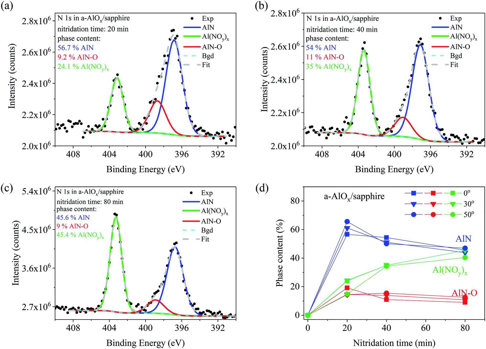 | ||
| Fig. 4 Analysis of chemical bonding of nitrogen in the a-AlOx buffer layer on sapphire substrate after nitridation for (a) 20 min, (b) 40 min and (c) 80 min. The XPS spectra were measured at the angle of 0°. Concentration of each compound is indicated in the plots. (d) Dependence of AlN, AlN–O, and Al(NOy)x phase concentrations on the nitridation time for detection angles of 0° (squares), 30° (triangles), and 50° (circles). | ||
In the bare c-plane sapphire sample (Fig. 2) the N 1s line can be deconvoluted into two components, with the binding energy differing by 2.3 eV. FWHM of these components decreases from 2.8 eV to 2.2 eV with the increase of nitridation time from 20 min to 80 min, which indicates improved chemical order around N atoms for longer annealing of the sample in nitrogen plasma. Also the relative contributions of both components change with the nitridation time. As shown in Fig. 2(a–c) the magnitude of the low energy component increases while that of the high energy component decreases for longer nitridation times. The binding energy of the low energy component is typical for AlN (396.7 eV).1,2,16,21,38–40 The higher energy peak is attributed to NO molecules formed in oxygen-rich environment after filling vacancies around Al in octahedral coordination and creation of the AlN–O oxinitride phase. The same chemical bonding of nitrogen in crystalline sapphire and similar changes with nitridation time of AlN and AlN–O phase contents have been observed already.1,21,40 Due to the small amount of nitrogen up-taken by crystalline sapphire the in-depth N distribution could be analyzed only in the sample nitridated for 80 min. As shown in Fig. 2(d) the surface concentrations of AlN and AlN–O phases are nearly equal. However, in the bulk of the sample more AlN than AlN–O was found. As will be explained later when discussing the microscopic model of nitrogen transport paths, this proves that the diffusion of N starts through oxygen vacancies at the surface and proceeds deeper forming first the oxinitride phase. A similar effect has been reported already in ref. 23.
Different nitridation chemistry was found for a-AlOx buffer layers deposited on Si and sapphire substrates (Fig. 3 and 4, respectively). Three chemical compounds were formed already after 20 min of nitridation on both substrates. Two of them are similar to those formed on sapphire, namely AlN and AlN–O, but now with a slightly smaller difference in binding energies (2–1.7 eV), while the third one corresponds to the line observed at a distance of 6.4 to 6.8 eV from the AlN-related N 1s line component. A similar line, but with a binding energy higher by 7 eV than that in AlN, was observed in sapphire after 0.5 keV N2+ ion bombardment.38 It was attributed to an Al(NOy)x compound, in which nitrogen is trapped in the cation-deficient lattice of sapphire on empty octahedral sites surrounded by oxygen atoms which should be bonded to Al.
As seen in Fig. 3(d) the content of the Al(NOy)x phase increases from 3.3 at% for 20 min up to 23.8 at% after 80 min of nitridation of the buffer on Si substrate. In the a-AlOx buffer on sapphire substrate the Al(NOy)x line is much stronger but it similarly increases with nitridation time starting from 24.1% for 20 min up to 45.4% for the sample treated in nitrogen plasma for 80 min (Fig. 4(c)). On both substrates the amount of the AlN–O oxinitride component slightly decreases during nitridation, similar to the dominant AlN component. The phase content changes for various detection angles indicate no pronounced differences in the depth distribution of the components in the buffer layers on Si and sapphire substrates. In both cases slightly more of the AlN–O component is found at the surface while the content of the Al(NOy)x phase is higher in the bulk.
Finally, the question arises as to what extent the presence of Mg Kα3 satellite line in the excitation X-ray radiation influences the data presented in Fig. 3 and 4. As mentioned in the experimental section the Mg Kα3 radiation generates an additional line at a distance of −8.3 eV and with the intensity of 8% of the main Mg Kα1,2 peak.28 In our spectra this satellite line repeats the Al(NOy)x peak so it slightly overlaps with the low energy part of the AlN peak, thus affecting the accuracy of the AlN content estimation. This is negligible if the amount of the Al(NOy)x phase is less than ∼10%, as in the case of short nitridation times of a-AlOx buffer on Si (Fig. 3a–b). There the uncertainty of AlN content determination is less than 1%. However, this does not apply for longer nitridation times and for a-AlOx buffers on sapphire. Then the content of Al(NOy)x phase reaches 45% increasing the error in estimation of AlN content up to 4% for 80 min long nitridation of a-AlOx buffer on sapphire (Fig. 4(c)). These corrections were not taken into account in the data presented in Fig. 3 and 4. Despite that, we underline that this effect does not affect the qualitative description of the phenomena presented in this work and its main conclusions.
In order to explain our experimental findings the crucial role of sample stoichiometry must be underlined, since it determines the way nitrogen from the plasma is incorporated into sapphire. As can be seen in Table 1 the main difference between chemical compositions of crystalline sapphire and a-AlOx samples before nitridation is the presence of O vacancies in crystalline sapphire (O/Al < 1.5) while Al vacancies dominate in the a-AlOx buffer layers (O/Al > 1.5). It has been pointed out in several papers that formation of nitride-type tetrahedral surroundings, starting from the octahedral one in sapphire, is accomplished in two stages: (i) oxygen vacancies should be present around the metal atoms, (ii) nitrogen atoms react with the oxygen-deficient metal clusters via a thermodynamically feasible process to form nitride-type bonds.38,41 This model has been tested for several metal oxides by studying implantation of N2+ ions38 and adsorption of nitrogen dioxide.41 Moreover, DFT calculations of N 1s core electron binding energies have been performed for a number of nitrogen-containing species in several oxidation states.41 In the case of bare crystalline sapphire the oxygen vacancies are present at the surface, so during nitridation the N atoms substitute for these vacancies to bond with aluminum forming the AlN–O phase. The binding energy for such NO− species is ∼400 eV,41 in agreement with the position of the high energy component in the N 1s spectra presented in Fig. 2(a–c). There are reports that AlN–O was detected as the major phase at the surface of crystalline sapphire when the nitridation temperature was low.21 However, almost equal amounts of AlN and AlN–O compounds were observed at the top of the sample after high temperature nitridation. This is exactly what we found after 20 min of nitridation at 800 °C (see Fig. 2(d)). For longer nitridation times the AlN phase dominated, indicating that N diffused into the bulk of the film forming tetrahedrally coordinated AlN there, while the oxygen atoms replaced by nitrogen diffused out to the surface. The overall rate of such a process is determined by the diffusion rate of the slower of the two moving anions. Earlier XPS studies have shown that the chemical diffusion coefficient of nitrogen is higher than that of oxygen.40 Therefore, the overall nitridation rate is expected to be controlled by the out-diffusion of oxygen to the surface.20,40 This explains well our finding that after 80 min long nitridation the surface concentrations of AlN and AlN–O phases were nearly equal, while more AlN than AlN–O was detected in the bulk of the sample (see Fig. 2(d)). This explanation also follows the one proposed in ref. 39.
The situation is quite different for a-AlOx buffer layers in which, independently of the substrate, significant Al deficiency is found before nitridation. This opens a new path for nitrogen incorporation, more effective than in c-Al2O3. Specifically, the N atoms can be trapped in empty octahedral sites of Al vacancies surrounded by oxygen atoms and form a compound similar to Al(NOy)x. The formation of such a compound was observed already when the over-stoichiometric surface of crystalline sapphire (O/Al > 1.5) was bombarded by low energy N2+ ions.38 The ion bombardment was used to create oxygen vacancies. However, for low ion beam energy, i.e., before O vacancies were formed, only the N 1s line of the Al(NOy)x phase was found at the energy of 403.6 eV. Formation of AlN and AlN–O started when the O/Al ratio reached a value smaller than 1.5, which indicates the crucial role of oxygen vacancies in the formation of these phases. It is noteworthy that a similar process may well explain the creation of the third compound in a-AlOx buffers containing initially Al vacancies. The formation of Al(NOy)x efficiently creates O vacancies because each N atom binds more than one O atom. For example, in the case of y = 3 and x = 3 each Al atom is bonded with three NO3 molecules. The N 1s line of such a molecule occurs at a binding energy of 407.4 eV, while the binding energy of the NO2 molecule is 403.6 eV,41 i.e., very close to that found in our studies. The necessary condition to start this process is the presence of Al vacancies. Then the effective consumption of excess oxygen by the formation of the Al(NOy)x compound introduces O vacancies, which allows further nitrogen incorporation via creation of AlN-type bonding. This process leads to formation of AlN with much lower amount of the oxinitride fraction than in the case of crystalline sapphire. The above model explains also properly our finding that much more N was incorporated into a-AlOx buffers on Si (up to 15.2 at%) than on sapphire (up to 6 at%) substrates (Fig. 1), while much more of the Al(NOy)x compound was formed in the latter sample (compare Fig. 3(d) and 4(d)). Indeed, this indicates that more O vacancies were created in the a-AlOx buffer on Si substrate since the buffer layer was the sole source of oxygen. On the contrary, in a-AlOx/sapphire structures the sapphire substrate itself was an unlimited reservoir of oxygen which might diffuse to the buffer layer making the creation of O vacancies less effective and thus limiting the up-take of nitrogen from the plasma. Finally, it is worth mentioning that the supply of oxygen from the sapphire substrate explains also the different dependencies of the O/Al ratio on the detection angle shown in Table 1 for a-AlOx films on Si and sapphire substrates. In a-AlOx/Si structures oxygen vacancies are formed at the surface (detection angles of 30° and 55°) already after 20 min of nitridation while for the films on sapphire the O/Al ratio remains close to the stoichiometric value of 1.5 due to delivery of oxygen from the substrate.
Conclusions
The XPS technique was used to determine the chemical state and in-depth distribution of nitrogen after nitridation of sapphire in nitrogen plasma. The nitridation was performed at 800 °C on crystalline sapphire (c-Al2O3) and on 15 nm thick, amorphous a-AlOx layers deposited by ALD on Si and sapphire substrates to compare interaction of active nitrogen with these surfaces. We show that under the same conditions of plasma treatment the results of nitridation are significantly different for crystalline sapphire and a-AlOx samples, which we correlate with the initial stoichiometry of both materials. At the surface of crystalline sapphire O vacancies were found before nitridation, which are considered to be necessary for formation of AlN-type bonding. The process proceeded via diffusion limited continuous replacement of oxygen atoms by nitrogen. It was quite slow and involved formation of the oxinitride AlN–O phase. After 80 min of nitridation only ∼3.4 at% of N was incorporated. In contrast, in a-AlOx layers Al vacancies were present at the surface before nitridation. Therefore, nitrogen incorporation started with accumulation of N in the cation-deficient lattice, in empty octahedral sites surrounded by oxygen atoms, leading to creation of NOx molecules and the Al(NOy)x phase. Since the Al(NOy)x compound efficiently consumed the excess oxygen, more O vacancies than occurring naturally at the crystalline sapphire surface were introduced, which in turn enhanced AlN and AlN–O formation. This scenario predicts more effective nitrogen incorporation into a-AlOx than into crystalline sapphire samples. Indeed, up to 3.3 at% and 7 at% of N was accumulated in the a-AlOx/sapphire and a-AlOx/Si structures, respectively, but only 0.8 at% in crystalline sapphire after 20 min of nitridation under the same conditions. 57% and 82% of the incorporated N ions contributed to the formation of AlN bonds in a-AlOx/sapphire and a-AlOx/Si structures, respectively. Extended nitridation time did not increase the amount of nitrogen incorporated in the AlN and AlN–O phases. Instead, the amount of the Al(NOy)x compound increased, particularly in a-AlOx/sapphire structures where the substrate was the unlimited suppliant of oxygen.Conflicts of interest
The authors declare no conflicts of interest.Acknowledgements
The authors are grateful to H. Przybylinska for careful reading the manuscript. This work was supported by the Polish National Science Centre grant 2016/23/B/ST7/03745.References
- G. V. Soares, K. P. Bastos, R. P. Pezzi, L. Miotti, C. E. Driemeier, I. J. R. Baumvol, C. L. Hinkle and G. Lucovsky, Appl. Phys. Lett., 2004, 84, 4992 CrossRef CAS.
- H. Y. Chen, H. L. Lu, J. X. Chen, F. Zhang, X. M. Ji, W. J. Liu, X. F. Yang and D. W. Zhang, ACS Appl. Mater. Interfaces, 2017, 9, 38662 CrossRef CAS PubMed.
- H. Jiang, Z. Yin, P. Tai-Song, Z. Bo, H. Guo-Hua and L. Yuan, Chin. Phys. B, 2012, 21, 126501 CrossRef.
- D. J. Lee, J. W. Lim, J. K. Mun and S. J. Yun, Mater. Res. Bull., 2016, 83, 597 CrossRef CAS.
- H. Lee, K. Ueda, Y. Enomoto, K. Arafune, H. Yoshida, S. Satoh, T. Chikyow and A. Ogura, Jpn. J. Appl. Phys., 2015, 54, 08KD18 CrossRef.
- Y. J. Cho, H. Cha and H. S. Chang, Surf. Coat. Technol., 2016, 307, 1096 CrossRef CAS.
- C. H. Shin, D. W. Kwak, D. H. Kim, D. W. Lee, S. Huh, K. S. Park and H. Y. Cho, 35th IEEE Photovoltaic Specialists Conference 003114–003117, 2010, DOI:10.1109/PVSC.2010.5614520.
- M. Sobanska, K. Klosek, J. Borysiuk, S. Kret, G. Tchutchulashvili, S. Gieraltowska and Z. R. Zytkiewicz, J. Appl. Phys., 2014, 115, 043517 CrossRef.
- M. Sobanska, Z. R. Zytkiewicz, K. Klosek, R. Kruszka, K. Golaszewska, M. Ekielski and S. Gieraltowska, Nanotechnology, 2020, 31, 184001 CrossRef PubMed.
- M. Sobanska, K. P. Korona, Z. R. Zytkiewicz, K. Klosek and G. Tchutchulashvili, J. Appl. Phys., 2015, 118, 184303 CrossRef.
- M. Sobanska, S. Fernández-Garrido, Z. R. Zytkiewicz, G. Tchutchulashvili, S. Gieraltowska, O. Brandt and L. Geelhaar, Nanotechnology, 2016, 27, 325601 CrossRef CAS PubMed.
- M. Sobanska, Z. R. Zytkiewicz, G. Calabrese, L. Geelhaar and S. Fernández-Garrido, Nanotechnology, 2019, 30, 154002 CrossRef CAS PubMed.
- M. Sobanska, V. G. Dubrovskii, G. Tchutchulashvili, K. Klosek and Z. R. Zytkiewicz, Cryst. Growth Des., 2016, 16, 7205 CrossRef CAS.
- L. Geelhaar, H. T. Grahn and O. Brandt, Phys. Rev. B: Condens. Matter Mater. Phys., 2014, 90, 195309 CrossRef.
- V. Miikkulainen, M. Leskela, M. Ritala and R. L. Puurunen, J. Appl. Phys., 2013, 113, 021301 CrossRef.
- G. Namkoong, W. A. Doolittle and A. S. Brown, J. Appl. Phys., 2002, 91, 2499 CrossRef CAS.
- K. Uchida, A. Watanabe, F. Yano, M. Kouguchi, T. Tanaka and S. Minagawa, J. Appl. Phys., 1996, 79, 3487 CrossRef CAS.
- T. Hashimoto, J. Appl. Phys., 1999, 86, 3670 CrossRef CAS.
- S. Shetty, J. Ghatak and S. M. Shivaprasad, Solid State Commun., 2014, 180, 7 CrossRef CAS.
- Y. Cho, Y. Kim, E. R. Weber, S. Ruvimov and Z. Liliental-Weber, J. Appl. Phys., 1999, 85, 7909 CrossRef CAS.
- M. Losurdo, P. Capezzuto, G. Bruno, G. Namkoong, W. A. Doolittle and A. S. Brown, J. Appl. Phys., 2002, 91, 2508 CrossRef CAS.
- C. M. Fang, R. Metselaar, H. T. Hintzen and G. de With, J. Am. Ceram. Soc., 2001, 84, 2633 CrossRef CAS.
- J. W. McCauley, P. Patel, M. Chen, G. Gilde, E. Strassburger, B. Paliwal, K. T. Ramesh and D. P. Dandekar, J. Eur. Ceram. Soc., 2009, 29, 223 CrossRef CAS.
- S. Gieraltowska, L. Wachnicki, B. S. Witkowski, R. Mroczynski, P. Dluzewski and M. Godlewski, Thin Solid Films, 2015, 577, 97 CrossRef CAS.
- S. Ino, Jpn. J. Appl. Phys., 1977, 16, 891–908 CrossRef CAS.
- N. Osakabe, K. Yagi and G. Honjo, Jpn. J. Appl. Phys., 1980, 19, L309–L312 CrossRef CAS.
- K. Klosek, M. Sobanska, G. Tchutchulashvili, Z. R. Zytkiewicz, H. Teisseyre and L. Klopotowski, Thin Solid Films, 2013, 534, 107 CrossRef CAS.
- M. O. Krause and J. G. Ferreira, J. Phys. B: At. Mol. Phys., 1975, 8, 2007 CrossRef CAS.
- N. Fairley, Casa Software Ltd version 2.3.17 Search PubMed.
- M. P. Seah, I. S. Gilmore and S. J. Spencer, J. Electron Spectrosc. Relat. Phenom., 2001, 120, 93 CrossRef CAS.
- S. Tanuma, Surf. Interface Anal., 2006, 38, 178 CrossRef CAS.
- http://www.npl.co.uk/nanoanalysis/a1calib.html-resource.npl.co.uknanoanalysisxpsamrsf, Factors (AMRSFs) for X-ray Photoelectron Spectroscopy (XPS).pdf Search PubMed.
- K. P. Bastos, R. Pezzi, L. Miotti, G. Soares, C. Driemeier, J. Morais, I. J. R. Baumvol, C. Hinkle and G. Lucovsky, Appl. Phys. Lett., 2004, 84, 97 CrossRef CAS.
- Y. Yao, T. Sekiguchi, T. Ohgaki, Y. Adachi and N. Ohashi, J. Ceram. Soc. Jpn., 2012, 120, 513 CrossRef CAS.
- S. Shetty, J. Ghatak and S. M. Shivaprasad, Solid State Commun., 2014, 180, 7 CrossRef CAS.
- A. Georgakilas, S. Mikroulis, V. Cimalla, M. Zervos, A. Kostopoulos, Ph. Komninou, Th. Kehagias and Th. Karakostas, Phys. Status Solidi A, 2001, 188, 567 CrossRef CAS.
- A. J. Ptak, K. S. Ziemer, M. R. Millecchia, C. D. Stinespring and T. H. Myers, MRS Internet J. Nitride Semicond. Res., 1999, 4(S1), G3.10 CrossRef.
- J. P. Espinós, A. R. González-Elipe, M. Mohai and I. Bertóti, Surf. Interface Anal., 2000, 30, 90 CrossRef.
- M. Losurdo, P. Capezzuto and G. Bruno, J. Appl. Phys., 2000, 88, 2138 CrossRef CAS.
- F. Dwikusuma and T. F. Kuech, J. Appl. Phys., 2003, 94, 5656 CrossRef CAS.
- J. Baltrusaitis, P. M. Jayaweera and V. H. Grassian, Phys. Chem. Chem. Phys., 2009, 11, 8295 RSC.
| This journal is © The Royal Society of Chemistry 2020 |