DOI:
10.1039/D0RA04744A
(Paper)
RSC Adv., 2020,
10, 28492-28500
Studies on interstitial carbon doping from a Ti precursor in a hierarchical TiO2 nanostructured photoanode by a single step hydrothermal route†
Received
29th May 2020
, Accepted 20th July 2020
First published on 3rd August 2020
Abstract
Carbon doping from a Ti precursor in TiO2 synthesized by a hydrothermal method was studied. The structural, optical and morphological study of the deposited material was carried out using X-ray diffraction, UV-vis spectroscopy and scanning electron microscopy characterization techniques. The elemental composition of the TiO2 deposited with different precursor concentrations was studied using X-ray photoelectron spectroscopy and electron dispersive X-ray spectroscopy. The amount of elemental carbon in the TiO2 matrix is found to be increased as the Ti precursor concentration is increased, which strengthens the proposed idea of carbon doping via a Ti precursor.
1. Introduction
A photoelectrochemical cell (PEC) is one of the best ways by which the abundant solar energy can be efficiently converted into electricity, and can be used to convert solar energy into any useful energy fuels by means of photocatalysis. A large number of materials which can be employed as a photoactive material in PECs have been investigated over the years, and out of these TiO2 seems to be the most promising material due to its high efficiency, low cost, chemical inertness, eco-friendly nature and photostability.1–3 However, the ability of this material is greatly limited by its low light harvesting in the visible region because of its wide band gap (for the rutile phase: 3.0 eV and for the anatase phase: 3.2 eV). Therefore, there has been much effort to enhance the visible light harvesting capacity of TiO2. One way is to sensitize the electrode surface with some sort of semiconducting material which has a band gap in the visible region. This technique is not so popular when a photoelectrode is used for the water splitting application, because the sensitization causes burying of the active catalysis sites on the surface. The other way of enhancing the visible light harvesting capacity of the TiO2 material is band gap tuning by introducing various types of impurities into the matrix of the material, i.e., by doping impurities into the TiO2 matrix. This doping causes an effective decrease in the band gap energy of TiO2 and this finally leads to increased visible light harvesting. There are numerous methods (such as metalorganic chemical vapour deposition (MOCVD), oblique-angle electron beam deposition, glancing angle deposition (GLAD) and so on) which have been reported for the synthesis of different TiO2 nanostructures.4–7 Among these methods, a hydrothermal method proved to be the best for the synthesis of TiO2 nanostructures, because this method allows the production of the said material in an environmentally benign and simple way. This method also allows the easy alteration of the properties of materials such as crystallite size and morphology at a nanoscale by simply changing the synthesis parameters, such as reaction temperature, precursor concentration, pH and so on.
As discussed previously, the doping of the TiO2 material allows the tuning of the band gap of TiO2, which makes it possible for this material to harvest the visible part of the solar spectrum. There are several reports where a red shift in the band gap energy of TiO2 is reported. In most of the papers, pure TiO2 was doped with different non-metal impurities such as N, S or C and so on.8–22 In the present investigation there has been no intentional doping of any of the previously mentioned elements. However, one thing that has been deliberately investigated, is the possibility of incorporation of carbon from the starting material, i.e., titanium(IV) isopropoxide (TTIP). The researchers particularly in the field of photocatalysis have thoroughly investigated the role of carbon in the TiO2 matrix and the red shift observed in the band gap energy.8–18 In order to explain the red shift observed in the system described in this paper, some of the most related experimental and theoretical works have been referred.9–11,17,18,23–35 This paper particularly reports about the results obtained during the investigation of carbon doping from a Ti precursor. These results are the first of their kind because as far as is known up to now no one has reported such a focused study on doping of carbon from a Ti precursor. It is felt that this report will open a new avenue for researchers to tune the band gap of TiO2 and will also pave the way for the creation of simultaneous doping and sensitization for an effective working photoanode for a variety of photoelectric applications.
So, the present manuscript reports on the possibility of carbon doping from a Ti precursor and the supporting characterization results; for example, X-ray diffraction (XRD) confirms the rutile phase of TiO2, X-ray photoelectron spectroscopy (XPS) confirms the presence of carbon in the TiO2 lattice, electron dispersive X-ray spectroscopy (EDS) confirms the relationship of the precursor concentration to the carbon doping, and finally, optical studies confirm the actual band gap tuning of the material.
2. Experimental details
2.1. Thin film deposition
The TiO2 was synthesised by the method reported previously by Burungale et al., with some modifications.36 The chemicals used were titanium(IV) isopropoxide (C12H28O4Ti) (99.98%, Alfa Aesar), and concentrated HCl (35.46%, Thomas Baker). Distilled water was used to prepare aqueous solutions. The F:SnO2 (FTO) coated glass plates (∼12 Ω cm−1, 1 cm × 3.5 cm) were used as substrates or supports for the TiO2 films for the photoelectrochemical measurements.
In a typical experiment the hydrothermal inorganic precursor solution was prepared by mixing different amounts of TTIP (i.e., 0.3 ml, 0.4 ml, 0.5 ml, 0.6 ml, 0.7 ml) in 10 ml of HCl and 10 ml of double distilled water. The samples were designated as T0.3, T0.4, T0.5, T0.6 and T0.7, respectively. The solution was then added into the Teflon lined stainless steel autoclave (with a capacity of 50 ml) containing FTO (conducting side facing up). Subsequently, the autoclave was maintained at 180 °C temperature for 3 h. The reaction time and reaction temperature were kept constant for all the experiments. The deposited thin films were annealed for 1 h at 450 °C.
2.2. Characterization of the TiO2 thin films
A D2 PHASER XRD diffractometer (Bruker AXS GmbH, Germany) was used to record the XRD patterns of the samples and the X'Pert PRO MRD (Malvern PANalytical) PW3388/60 at the Energy Convergence Core Facility at Chonnam National University was used for further analysis. The elemental information of the TiO2 thin film was obtained using XPS with a VG MultiLab 2000 (ThermoFisher Scientific, UK) with a microfocus monochromatic Al Kα X-ray source at high photonic energies from 0.1 keV to 3 keV. The elemental maps and compositional analysis of the nanocrystals were obtained using an EDS system attached to a JSM-7500F FE-SEM (Jeol, Japan). The room temperature optical absorption measurements were performed in the wavelength range of 190–1100 nm using a UV-1800 UV-vis spectrophotometer (Shimadzu, Japan). The surface morphology was examined using a JSM-6360 SEM (Jeol, Japan).
3. Results and discussion
3.1. X-ray diffraction
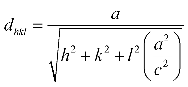
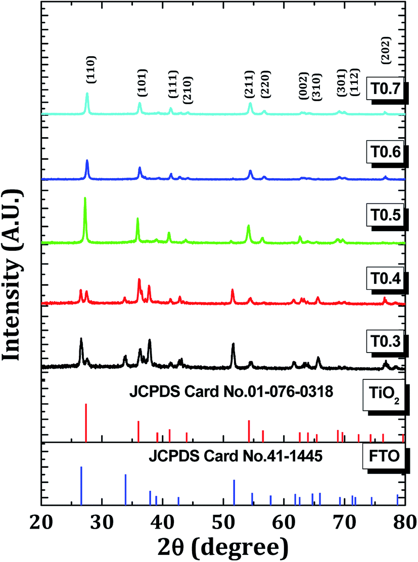
Fig. 1 shows the XRD patterns of all the TiO2 samples. The XRD patterns matched well with those on the JCPDS card no. 01-076-0318 which confirmed the rutile phase with a tetragonal crystal structure. All the samples, except for the T0.4 sample, were polycrystalline in nature with a major peak corresponding to the (110) plane. The lattice parameters ‘a’ and ‘c’ were calculated using the formula:37| |
 | (1) |
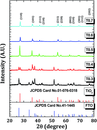 |
| | Fig. 1 The X-ray diffraction patterns of the T0.3, T0.4, T0.5, T0.6 and T0.7 samples. | |
The calculated values of the lattice parameters of all the samples were in good agreement with the standard lattice parameters of a = 4.508 Å and c = 3.027 Å which confirmed that the crystal system was tetragonal. By applying the Scherrer formula to the rutile (110) diffraction peaks, the average crystallite sizes of the samples were found to be 30, 35, 39, 36 and 30 nm for the samples T0.3, T0.4, T0.5, T0.6 and T0.7, respectively. Detailed XRD parameters are given in the Table 1.
Table 1 The detailed XRD parameters, for example, standard and calculated d values, standard and calculated values of the lattice parameters a, c and the corresponding crystallite sizes of all the TiO2 samples are summarized in this table
| Sample |
(hkl) plane |
Standard d (Å) |
Calculated d (Å) |
Standard |
Calculated |
Crystallite size (nm) |
| a (Å) |
c (Å) |
a (Å) |
c (Å) |
| T0.3 |
110 |
3.187 |
3.236 |
4.508 |
3.027 |
4.576 |
2.936 |
30 |
| T0.4 |
3.243 |
4.586 |
2.952 |
35 |
| T0.5 |
3.271 |
4.625 |
2.970 |
39 |
| T0.6 |
3.232 |
4.570 |
2.946 |
36 |
| T0.7 |
3.233 |
4.572 |
2.948 |
30 |
3.2. X-ray photoelectron spectroscopy
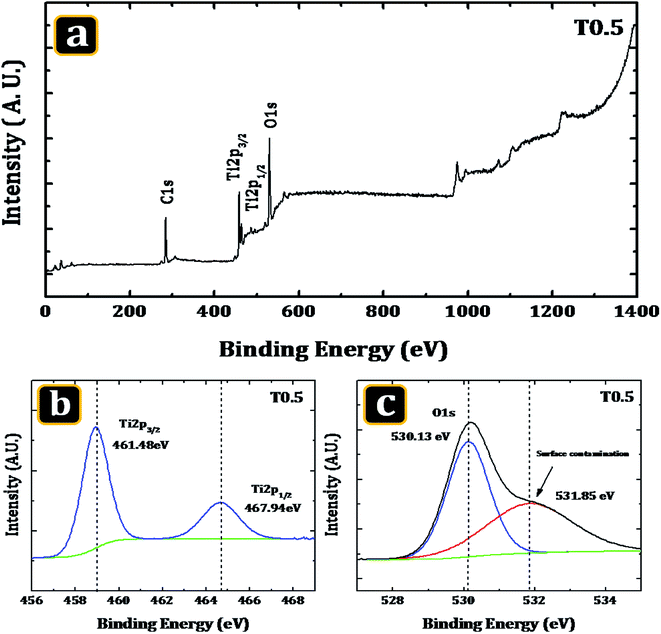
In order to confirm the elements present in the deposited material and also to verify the probability of carbon doping from the Ti precursor XPS was used. Fig. 2(a) shows the survey spectrum of the T0.5 sample and the high resolution XPS spectra of Ti (2p) and O (1s). The survey spectrum of the T0.5 sample revealed that the surface of the deposited material was composed mainly of Ti, O and a small amount of carbon. The presence of the carbon in the material may be due to two reasons: firstly it may be the adventitious carbon which generally accumulates on the surface of a sample when it was being exposed to the ambient atmosphere; secondly this may be the carbon introduced into the matrix of the TiO2 from the Ti precursor during the hydrothermal synthesis.
 |
| | Fig. 2 The XPS spectra of the T0.5 sample. (a) A representative XPS survey of the sample showing the intense core-level lines of Ti, (b) the Ti (2p) core level spectrum and (c) curve fit of the O (1s) peak. | |
Fig. 2(b) and (c) show a high-resolution scan of TiO2 in the Ti (2p) and O (s) region. The two peak structure observed in the high-resolution spectrum of Ti (2p) suggest the presence of Ti in the material. The features of the double peaks of Ti (2p3/2) and Ti (2p1/2), were accurately determined by decomposing the Ti (2p) XPS spectrum of the T0.5 sample with a Voigt curve fitting function inside the Shirley background. The decomposition of the Ti (2p) spectrum resulted in two peaks. These two decomposed peaks of the sample T0.5 were located at the binding energies of 461.48 eV and 467.94 eV. The peaks were related to the Ti (2p3/2) and Ti (2p1/2) core levels, respectively, of the Ti4+ cations of the TiO2 crystal structure. The considerable dislocation was not observed in the previous peak positions. These peak positions are similar to those reported by Pawar et al.38 for TiO2 thin films. The energy separation between these two peaks was 6.46 eV, which was comparable to that observed in a TiO2 nanomaterial by Thind et al.39 Similarly, Fig. 2(c) shows a compound double peak structure in the O (1s) spectrum of the T0.5 sample, suggesting the presence of the O element in the TiO2 rutile nanorods. A major O (1s) peak coupled with a small shoulder was observed. The two peaks, a strong peak having a centre at 530.13 eV and a little peak at 531.85 eV, resulted from the decomposition of the O (1s) spectrum. No considerable displacement of position was observed in case of peak. A strong peak observed in the spectra which was related to the O2− anions is the characteristic peak of the TiO2. The modest peak observed at the neighbourhood of the intense oxygen [O (1s)] peak indicated surface contamination40–42 or the occurrence of O containing species, such as hydroxyl groups or molecules of water that were adsorbed on the surface of the sample.43
Next the possibility of carbon doping will be considered. According to the theoretical work done by Valentin et al.18 on anatase and rutile TiO2, there were three possible ways to include C atoms into the TiO2 lattice. The first one was to replace the lattice oxygen with a carbon and the second one was to replace a Ti atom with a C atom. Both of these mechanisms implied the rupture of the Ti–O bonds that must be replaced by the Ti–C or the C–O bonds. The third possibility assumes that there was a stabilized carbon in an interstitial position. As discussed also in the same work, the replacement of lattice oxygen with carbon or the presence of interstitial carbon may result in a series of localized occupied states in the band gap, which could explain the absorption edge shift observed experimentally for thin and nanostructured rutile films. But the replacement of Ti atoms by carbon did not result in any impurity states in the band gap. So, the replacement of Ti atoms by carbon atoms did not contribute to the decrease in the band gap of rutile TiO2. The presence of carbon species at different possible positions could be observed experimentally by using XPS.
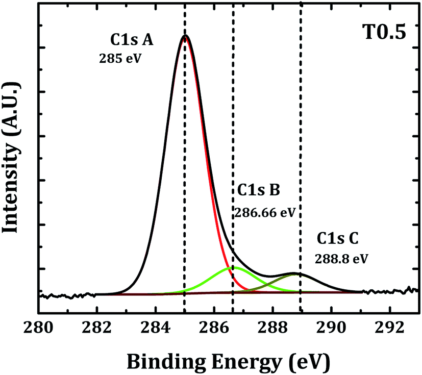
It is well documented that the peaks observed in the XPS survey spectrum of carbon doped TiO2, 458.4, 529.7 and 284.8 eV corresponded to Ti (2p3/2), O (1s), and C (1s) core levels, respectively.10,11,20,44,45 Generally, two peak structures at the binding energies of 284.8 and 288.6 eV were observed for the carbon-doped TiO2. The peak at 284.8 eV was thought to indicate the presence of adventitious elemental carbon and the peak at 286.6 eV indicated the presence of C–O bonds. If carbon was substituted for some of the lattice oxygen atoms and form a Ti–C structure then it showed a signature peak in the survey spectrum near 281.9 eV.23–25,27–29
In the present case the narrow scan spectrum of carbon in the TiO2 thin film (Fig. 3) shows three peaks at the binding energies 285, 286.6 and 288.8 eV. As discussed previously the peak at 285 eV may be due to the presence of adventitious elemental carbon and the peaks at 286.66 and 288.8 eV indicated the presence of C–O and C![[double bond, length as m-dash]](https://www.rsc.org/images/entities/char_e001.gif) O or Ti–O–C bonds.10,24,26,28,29,31,32,34,35 The absence of a peak near 281.9 eV confirmed that the substitution of carbon at Ti or O sites did not take place in our sample but the presence of peaks near 286.6 and 288.8 eV confirmed that the carbon was present in the TiO2 lattice in the form of carbonated species which is also referred to as interstitial doping.31–33,35 The decrease in the band gap of rutile TiO2 observed in the present investigation may be due to the interstitial carbon doping in the TiO2 lattice.
O or Ti–O–C bonds.10,24,26,28,29,31,32,34,35 The absence of a peak near 281.9 eV confirmed that the substitution of carbon at Ti or O sites did not take place in our sample but the presence of peaks near 286.6 and 288.8 eV confirmed that the carbon was present in the TiO2 lattice in the form of carbonated species which is also referred to as interstitial doping.31–33,35 The decrease in the band gap of rutile TiO2 observed in the present investigation may be due to the interstitial carbon doping in the TiO2 lattice.
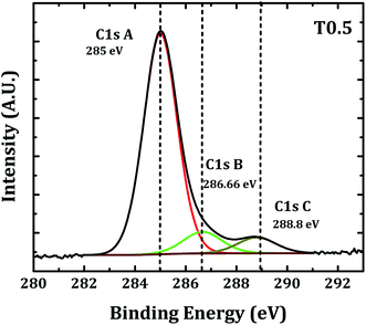 |
| | Fig. 3 Curve fitting of the C (1s) peak. | |
3.3. Electron dispersive X-ray spectroscopy
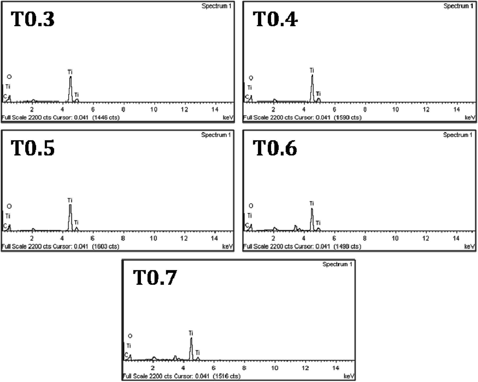
Further investigations regarding the presence of doped carbon in the matrix of TiO2 from Ti precursor, were carried out using EDS and the spectra of all samples can be seen in Fig. 4. Details of the atomic mass and weight% of the Ti, O and C elements in each sample are given in Table 2. From the results it was observed that the weight percentage of C in the T0.3 to T0.7 samples was 1.27, 1.60, 1.97, 2.73 and 3.21, respectively, whereas the atomic mass percentage of C was 2.82, 3.68, 4.43, 5.93 and 7.10, respectively. These values of weight and atomic mass percentage of carbon in the T0.3 to T0.7 samples suggested that the percentage of carbon continued to increase as the Ti precursor concentration increased. So, by increasing the Ti precursor concentration, a greater amount of carbon may be introduced or doped into the TiO2 matrix. In this way, the observed EDS results of elemental composition also strengthen the assumption that the carbon doping arises from the Ti precursor. The elemental mapping of all the TiO2 samples for the elements Ti, O and C is also given in Fig. 5.
 |
| | Fig. 4 The EDS spectra of the T0.3, T0.4, T0.5, T0.6 and T0.7 samples. | |
Table 2 Details of atomic mass and weight% of Ti, O and C elements in all the TiO2 samples
| Sample |
Elements |
Totals |
| C K |
O K |
Ti K |
| Weight% |
Atomic mass% |
Weight% |
Atomic mass% |
Weight% |
Atomic mass% |
| T0.3 |
1.27 |
2.82 |
37.70 |
63.07 |
61.04 |
34.11 |
100.00 |
| T0.4 |
1.60 |
3.68 |
34.24 |
59.24 |
64.16 |
37.08 |
100.00 |
| T0.5 |
1.97 |
4.43 |
35.71 |
60.37 |
62.32 |
35.19 |
100.00 |
| T0.6 |
2.73 |
5.93 |
37.73 |
61.60 |
59.54 |
32.47 |
100.00 |
| T0.7 |
3.21 |
7.10 |
35.50 |
58.92 |
61.29 |
33.98 |
100.00 |
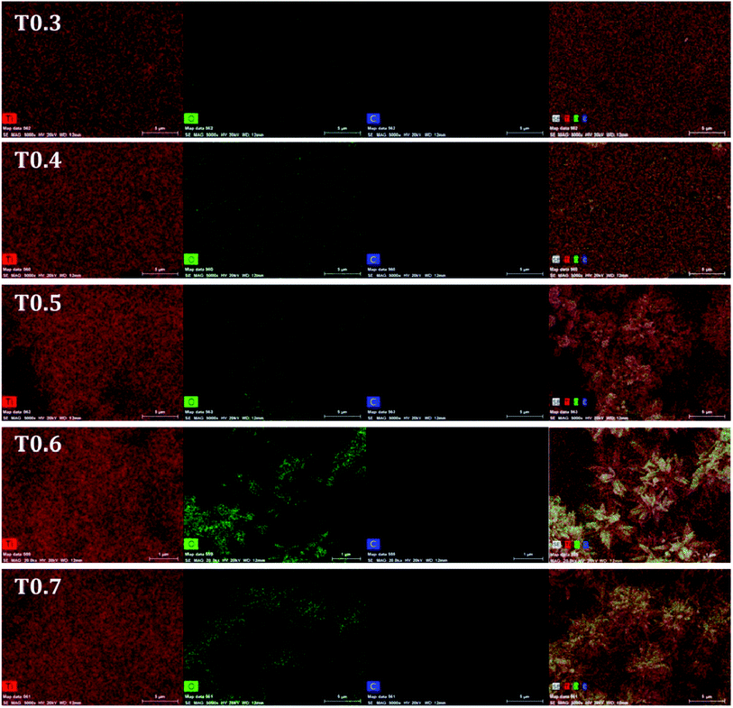 |
| | Fig. 5 The elemental mapping images of the T0.3, T0.4, T0.5, T0.6 and T0.7 samples for Ti, O and C elements. | |
3.4. Optical absorption
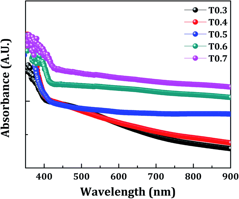
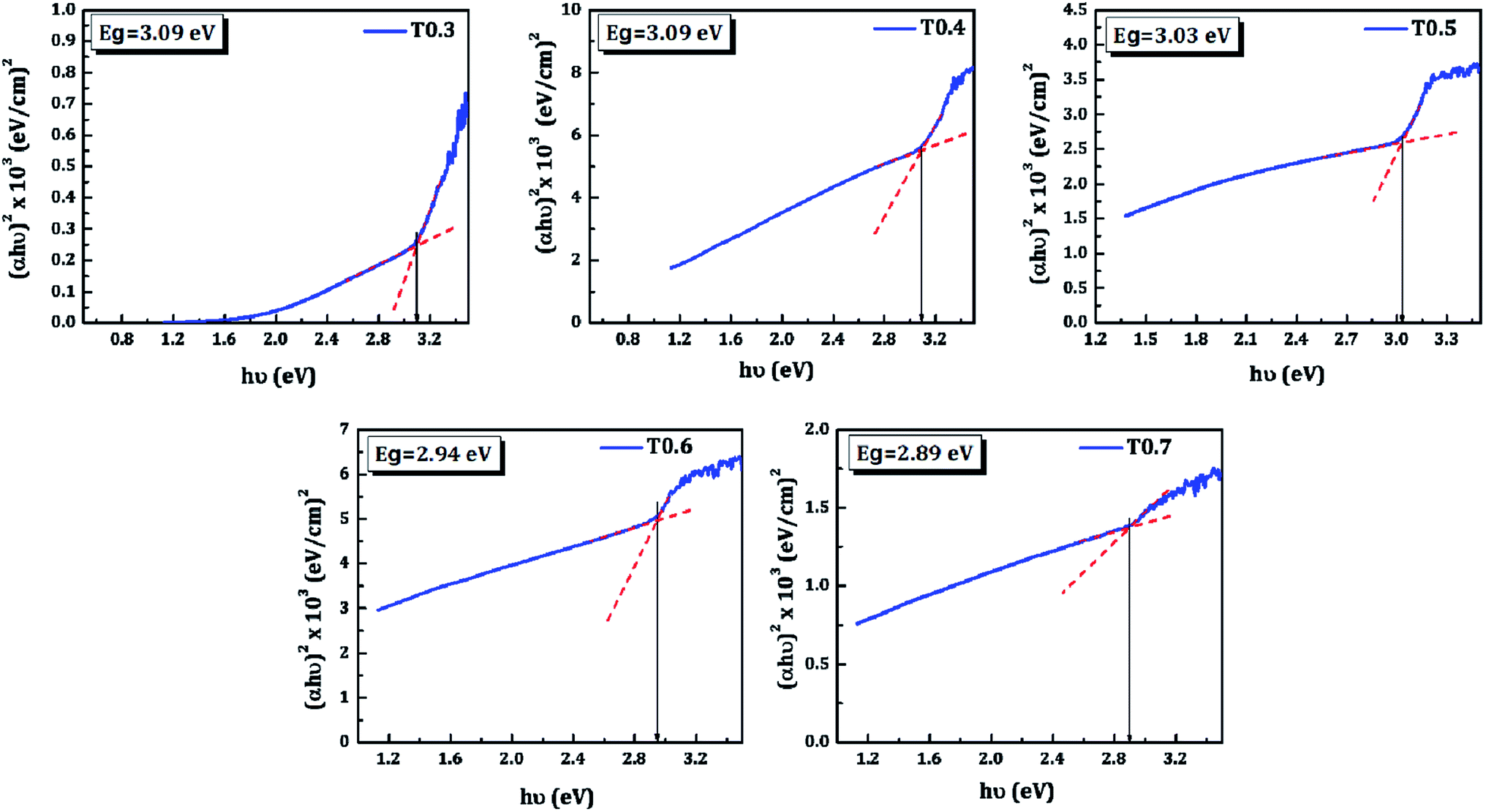
The band gap energy (Eg), the type of transition, and the absorption coefficient (α) of TiO2 thin films was determined from the optical absorption spectra shown in Fig. 6, which lie mainly in the UV region due to its wide band gap. The absorption coefficient can be expressed by eqn (2):where, α is the absorption coefficient, hν is photon energy, Eg is band gap energy, and α0 is a constant. The band gap energy was estimated by extrapolating the straight portion of (αhν)1/2 versus photon energy (hν), as shown in Fig. 7, and this indicates indirect and allowed optical transition. The values obtained for the band gap energy varied between 3.09–2.89 eV, thus a change was also observed in the band gap of TiO2 upon variations of the Ti precursor concentration. As discussed in the XPS and EDS section this decrease in the band gap of the deposited TiO2 material may be due to the presence of carbon in the matrix of the same material. In the present investigation the presence of carbon was observed in the XPS and EDS spectra, and the band gap energy was also decreased with variations in the Ti precursor concentration. So, the correlation of above three observations allows the assumption that there may be doping of the carbon from the starting material, i.e., the Ti precursor and the doping increases with an increase in the Ti precursor concentration.
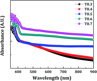 |
| | Fig. 6 The room temperature UV-visible absorption spectra of the samples T0.3, T0.4, T0.5, T0.6 and T0.7. | |
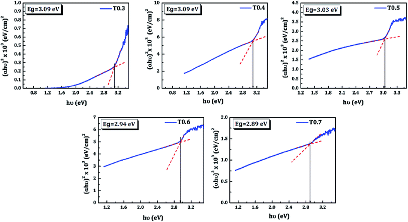 |
| | Fig. 7 The (αhν)1/2 versus hν plots of the TiO2 thin films. | |
3.5. Scanning electron microscopy
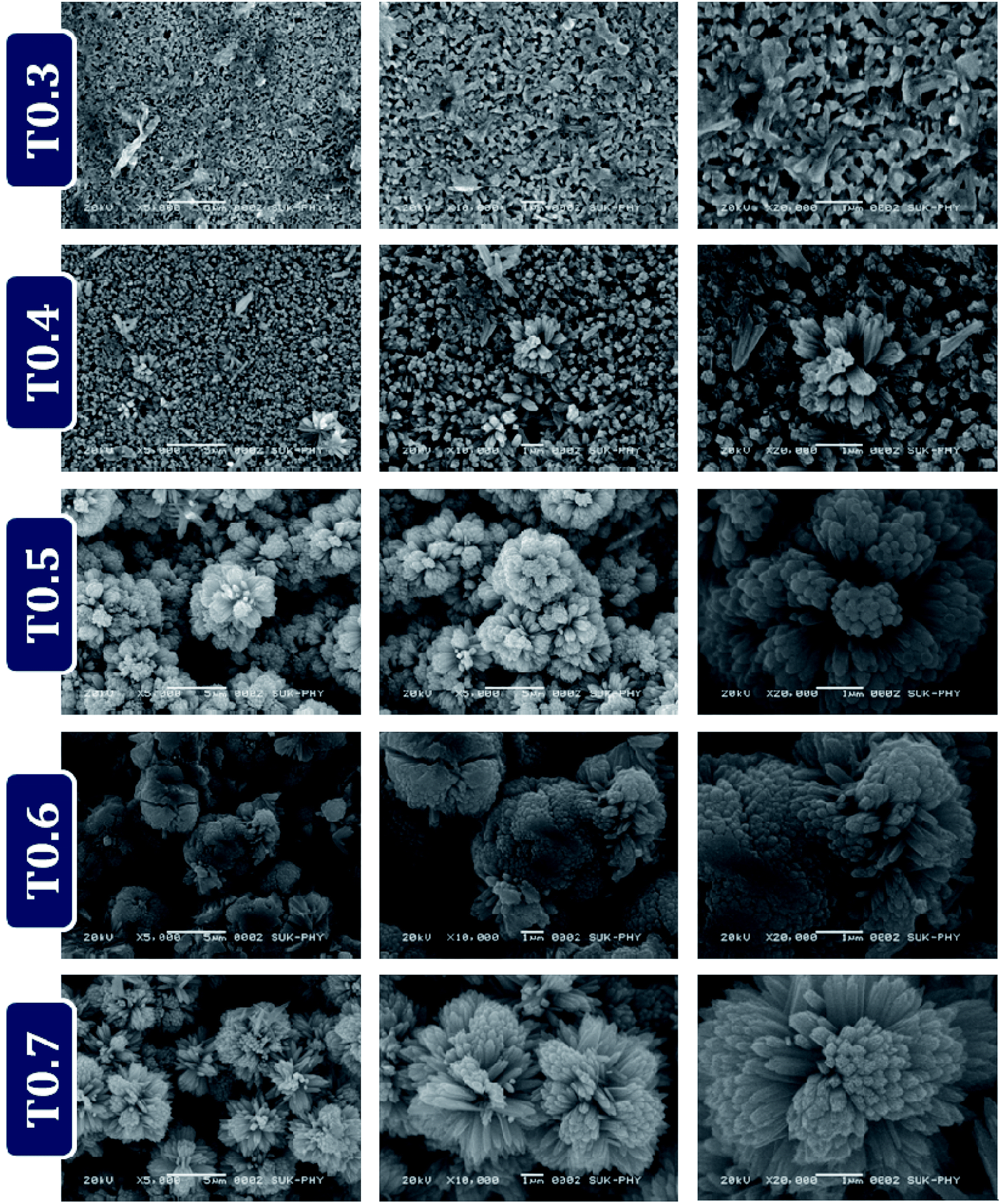
The SEM images in Fig. 8 show the top view of the samples T0.3, T0.4, T0.5, T0.6 and T0.7 and Fig. S2 (ESI)† shows the cross-sectional images of respective samples. The growth mechanism related to the formation of TiO2 nanorods and hierarchical microflower like structures has been discussed thoroughly in previous reports,36,46,47 however it is also discussed briefly in the ESI† of this paper. The layer of compactly arranged TiO2 nanorods is clearly observed in the SEM images of the T0.3 sample. The TiO2 nanorods formed are about 1 μm long and they form the subsequent compact layer after FTO on the glass substrates. From the SEM images of T0.4 it is also observed that there are some homocentric but undeveloped TiO2 microflowers. The average thickness of the T0.3 sample is about 1.15 μm which due to the extra growth of the microflower like structures on the surface of T0.4, have an average thickness of about 2 μm. In the third group of images, the T0.5 sample shows TiO2 microflowers which have grown well, with 1–1.5 μm long TiO2 nanorods as the petals and this is clearly observed. The average diameter of the microflowers formed in the T0.5 sample is about 2–3 μm. This new layer was formed over the first compact layer of the vertically aligned TiO2 nanorods, which caused the increase in the film thickness, so the average film thickness of the T0.5 sample is about 11 ± 0.3 μm. When the precursor concentration was further increased there was formation of many layers of compact TiO2 microflowers of diameter 2–3 μm. Due to these microflowers the average thickness of the T0.6 samples increased up to 36 μm. In cross sectional images the stacking of 5–6 layers of microflowers is clearly observed. The extra addition in the concentration level of Ti precursor just results in a thicker film of TiO2, which maintains the basic structure of compact microflowers with a diameter of 2–3 μm. The average thickness of the T0.7 film was about 46 μm.
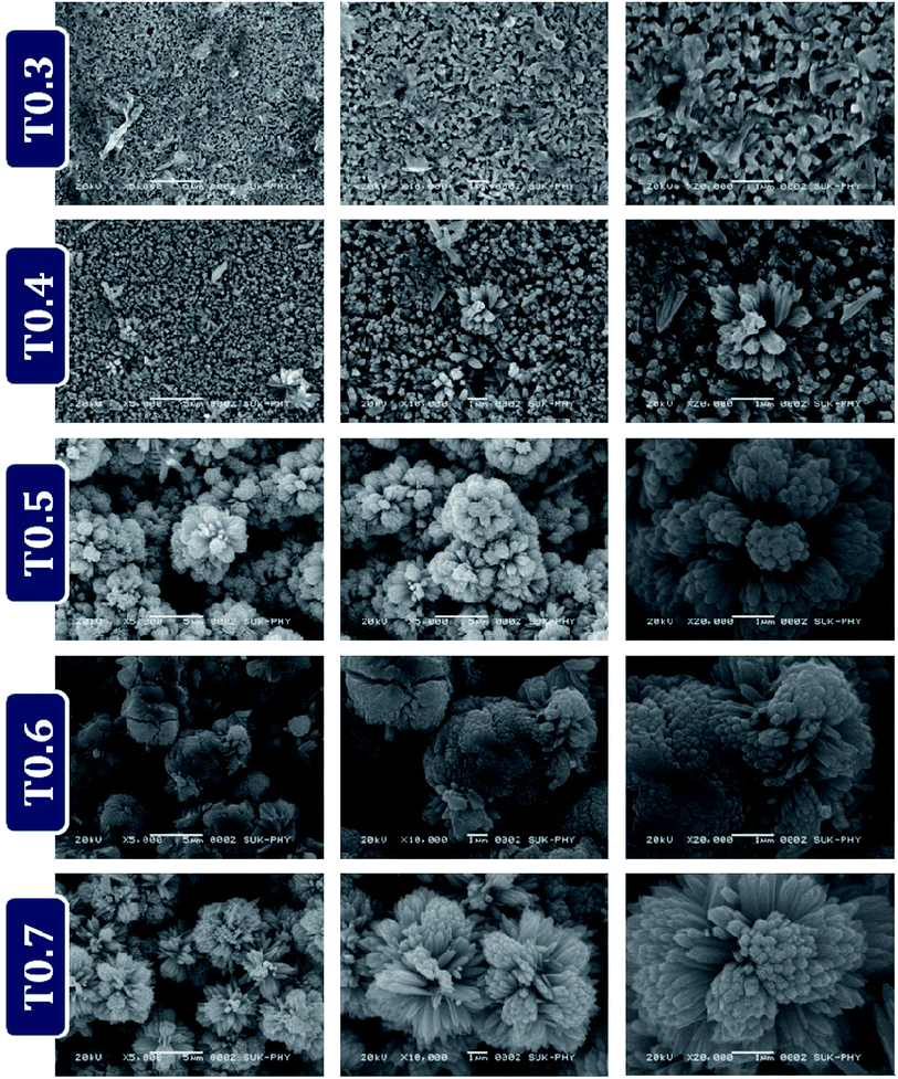 |
| | Fig. 8 The scanning electron microscopy images of the TiO2 samples at different magnifications. | |
4. Conclusions
In summary a TiO2 photoelectrode was successfully prepared with hierarchical rutile TiO2 nanostructures from a surfactant free, single step hydrothermal route. The effect of precursor concentration on the characteristics of the synthesized rutile TiO2 was studied and the correlation of precursor concentration and corresponding optical properties is also discussed systematically. In brief, the observed decrease in the band gap energy of the samples allows the assumption that there is a possibility of interstitial carbon doping from the Ti precursor and it is also observed that this doping goes on increasing with the increase in the Ti precursor concentration.
Conflicts of interest
There are no conflicts to declare.
Acknowledgements
This research was financially supported by the Ministry of Trade, Industry and Energy (MOTIE) and the Korea Institute for Advancement of Technology (KIAT) through the International Cooperative R&D Program (No. P0006851) and the Priority Research Centers Program through the National Research Foundation of Korea (NRF) funded by the Ministry of Education, Science and Technology (2018R1A6A1A03024334) and the Basic Science Research Capacity Enhancement Project through the Korea Basic Science Institute (Energy Convergence Core Facility) grant funded by the Ministry of Education.
References
- A. Fujishima and K. Honda, Nature, 1972, 238, 37–38 CrossRef CAS PubMed.
- B. Neumann, P. Bogdanoff, H. Tributsch, S. Sakthivel and H. Kisch, J. Phys. Chem. B, 2005, 109, 16579–16586 CrossRef CAS PubMed.
- H. Kisch, L. Zang, C. Lange, W. F. Maier, C. Antonius and D. Meissner, Angew. Chem., Int. Ed., 1998, 37, 3034–3036 CrossRef CAS.
- J.-J. Wu and C.-C. Yu, J. Phys. Chem. B, 2004, 108, 3377–3379 CrossRef CAS.
- J.-Q. Xi, J. K. Kim, E. F. Schubert, D. Ye, T.-M. Lu, S.-Y. Lin and J. S. Juneja, Opt. Lett., 2006, 31, 601 CrossRef CAS PubMed.
- J. Q. Xi, M. F. Schubert, J. K. Kim, E. F. Schubert, M. Chen, S. Y. Lin, W. Liu and J. A. Smart, Nat. Photonics, 2007, 1, 176–179 CrossRef CAS.
- Y. P. Zhao, D. X. Ye, G. C. Wang and T. M. Lu, Nano Lett., 2002, 2, 351–354 CrossRef CAS.
- S. Sakthivel and H. Kisch, Angew. Chem., Int. Ed., 2003, 42, 4908–4911 CrossRef CAS PubMed.
- S. U. M. Khan, M. Al-Shahry and W. B. Ingler, Science, 2002, 297, 2243–2245 CrossRef CAS PubMed.
- F. Dong, H. Wang and Z. Wu, J. Phys. Chem. C, 2009, 113, 16717–16723 CrossRef CAS.
- X. Wang, S. Meng, X. Zhang, H. Wang, W. Zhong and Q. Du, Chem. Phys. Lett., 2007, 444, 292–296 CrossRef CAS.
- S. Liu, L. Yang, S. Xu, S. Luo and Q. Cai, Electrochem. Commun., 2009, 11, 1748–1751 CrossRef CAS.
- J. H. Park, S. Kim and A. J. Bard, Nano Lett., 2006, 6, 24–28 CrossRef CAS PubMed.
- G. Wu, T. Nishikawa, B. Ohtani and A. Chen, Chem. Mater., 2007, 19, 4530–4537 CrossRef CAS.
- J. Zhong, F. Chen and J. Zhang, J. Phys. Chem. C, 2010, 114, 933–939 CrossRef CAS.
- H. Kamisaka, T. Adachi and K. Yamashita, J. Chem. Phys., 2005, 123, 084704 CrossRef PubMed.
- D. E. Gu, Y. Lu, B. C. Yang and Y. Da Hu, Chem. Commun., 2008, 2453–2455 RSC.
- C. Di Valentin, G. Pacchioni and A. Selloni, Chem. Mater., 2005, 17, 6656–6665 CrossRef CAS.
- J. Lu, Y. Dai, M. Guo, L. Yu, K. Lai and B. Huang, Appl. Phys. Lett., 2012, 100, 102114 CrossRef.
- J. Yang, H. Bai, Q. Jiang and J. Lian, Thin Solid Films, 2008, 516, 1736–1742 CrossRef CAS.
- X. Chen and C. Burda, J. Am. Chem. Soc., 2008, 130, 5018–5019 CrossRef CAS PubMed.
- R. Asahi, T. Morikawa, T. Ohwaki, K. Aoki and Y. Taga, Science, 2001, 293, 269–271 CrossRef CAS PubMed.
- P. A. Ochoa Rodríguez, T. B. Benzaquén, G. A. Pecchi, S. G. Casuscelli, V. R. Elías and G. A. Eimer, Materials, 2019, 12, 3349 CrossRef PubMed.
- R. Klaysri, M. Ratova, P. Praserthdam and P. J. Kelly, Nanomaterials, 2017, 7, 113 CrossRef PubMed.
- Z. Wu, F. Dong, W. Zhao, H. Wang, Y. Liu and B. Guan, Nanotechnology, 2009, 20, 2357501 Search PubMed.
- L. Ji, Y. Zhang, S. Miao, M. Gong and X. Liu, Carbon, 2017, 125, 544–550 CrossRef CAS.
- W. Mai, F. Wen, D. Xie, Y. Leng and Z. Mu, J. Adv. Ceram., 2014, 3, 49–55 CrossRef CAS.
- Y. Zhang, J. Chen, L. Hua, S. Li, X. Zhang, W. Sheng and S. Cao, J. Hazard. Mater., 2017, 340, 309–318 CrossRef CAS PubMed.
- J. Shao, W. Sheng, M. Wang, S. Li, J. Chen, Y. Zhang and S. Cao, Appl. Catal., B, 2017, 209, 311–319 CrossRef CAS.
- W. Li, R. Liang, N. Y. Zhou and Z. Pan, ACS Omega, 2020, 5, 10042–10051 CrossRef CAS PubMed.
- R. Purbia, R. Borah and S. Paria, Inorg. Chem., 2017, 56, 10107–10116 CrossRef CAS PubMed.
- D. Chen, Z. Jiang, J. Geng, Q. Wang and D. Yang, Ind. Eng. Chem. Res., 2007, 46, 2741–2746 CrossRef CAS.
- J. Liu, L. Han, H. Ma, H. Tian, J. Yang, Q. Zhang, B. J. Seligmann, S. Wang and J. Liu, Sci. Bull., 2016, 61, 1543–1550 CrossRef CAS.
- J. O. Tijani, O. O. Fatoba, T. C. Totito, W. D. Roos and L. F. Petrik, Carbon Lett., 2017, 22, 48–59 Search PubMed.
- J. Jia, D. Li, J. Wan and X. Yu, J. Ind. Eng. Chem., 2016, 33, 162–169 CrossRef CAS.
- V. V. Burungale, V. V. Satale, A. J. More, K. K. K. Sharma, A. S. Kamble, J. H. Kim and P. S. Patil, J. Colloid Interface Sci., 2016, 470, 108–116 CrossRef CAS PubMed.
- B. D. Cullity, Elements of X-ray Diffraction, Addison-Wesley Publishing Company, Inc., 1956 Search PubMed.
- S. A. Pawar, R. S. Devan, D. S. Patil, V. V. Burungale, T. S. Bhat, S. S. Mali, S. W. Shin, J. E. Ae, C. K. Hong, Y. R. Ma, J. H. Kim and P. S. Patil, Electrochim. Acta, 2014, 117, 470–479 CrossRef CAS.
- S. S. Thind, G. Wu, M. Tian and A. Chen, Nanotechnology, 2012, 23, 475706 CrossRef PubMed.
- J. A. Rengifo-Herrera, E. Mielczarski, J. Mielczarski, N. C. Castillo, J. Kiwi and C. Pulgarin, Appl. Catal., B, 2008, 84, 448–456 CrossRef CAS.
- R. S. Devan, W.-D. Ho, C.-H. Chen, H.-W. Shiu, C.-H. Ho, C.-L. Cheng, S. Y. Wu, Y. Liou and Y.-R. Ma, Nanotechnology, 2009, 20, 445708 CrossRef PubMed.
- R. S. Devan, W. Der Ho, S. Y. Wu and Y. R. Ma, J. Appl. Crystallogr., 2010, 43, 498–503 CrossRef CAS.
- R. S. Devan, C. L. Lin, S. Y. Gao, C. L. Cheng, Y. Liou and Y. R. Ma, Phys. Chem. Chem. Phys., 2011, 13, 13441–13446 RSC.
- C. S. Gopinath, S. G. Hegde, A. V. Ramaswamy and S. Mahapatra, Mater. Res. Bull., 2002, 37, 1323–1332 CrossRef CAS.
- E. Papirer, R. Lacroix, J. Donnet, G. Nanse and P. Fioux, Carbon, 1994, 32, 1341–1358 CrossRef CAS.
- V. V. Burungale, V. V. Satale, A. M. Teli, A. S. Kamble, J. H. Kim and P. S. Patil, J. Alloys Compd., 2016, 656, 491–499 CrossRef CAS.
- V. V. Burungale, H. Bae, A. S. Kamble, J. H. Kim, P. S. Patil and J. S. Ha, CrystEngComm, 2020, 22, 2462–2471 RSC.
Footnote |
| † Electronic supplementary information (ESI) available. See DOI: 10.1039/d0ra04744a |
|
| This journal is © The Royal Society of Chemistry 2020 |
Click here to see how this site uses Cookies. View our privacy policy here. 
 Open Access Article
 This Open Access Article is licensed under a Creative Commons Attribution-Non Commercial 3.0 Unported Licence
 c,
P. S. Patil*d and
J.-S. Ha
c,
P. S. Patil*d and
J.-S. Ha