
 Open Access Article
 This Open Access Article is licensed under a
 Creative Commons Attribution 3.0 Unported Licence
Optical optimization of double-side-textured monolithic perovskite–silicon tandem solar cells for improved light management
Fazal E. Subhan *ab,
Aimal Daud Khancd,
Adnan Daud Khana,
Najeeb Ullaha,
Muhammad Imrane and
Muhammad Nomana
*ab,
Aimal Daud Khancd,
Adnan Daud Khana,
Najeeb Ullaha,
Muhammad Imrane and
Muhammad Nomana
aUS-Pakistan Center for Advanced Studies in Energy, University of Engineering & Technology, Peshawar, 25000, Pakistan
bArizona State University, Tempe, Arizona 85287, USA. E-mail: fsubhan@asu.edu
cCollege of Energy, Soochow Institute for Energy and Materials Innovations (SIEMIS), Soochow University, Suzhou 215006, China
dKey Laboratory of Advanced Carbon Materials and Wearable Energy Technology of Jiangsu Province, Key Laboratory of Modern Optical Technologies of Ministry of Education, Suzhou 215006, China
eDepartment of Electrical Engineering, Military College of Signals, National University of Sciences and Technology (NUST), Islamabad, 46000, Pakistan
First published on 16th July 2020
Abstract
Tandem configuration-containing perovskite and silicon solar cells are promising candidates for realizing a high power conversion efficiency of 30% at reasonable costs. Silicon solar cells with planar front surfaces used in tandem devices cause high optical losses, which significantly affects their efficiency. Moreover, some studies have explored the fabrication of perovskites on textured silicon cells. However, due to improper texturing, light trapping is not ideal in these devices, which reduces the efficiency. In this work, we optimized the pyramid height of textured silicon cells and efficiently characterized them to achieve enhanced light trapping. Two different kinds of perovskites, namely, Cs0.17FA0.6Pb(Br0.17I0.7)3 and Cs0.25FA0.6Pb(Br0.20I0.7)3 with wide bandgaps were conformally deposited on textured silicon cells, and the performance of these flat and fully textured tandem devices was numerically analyzed. The thickness of each layer in the tandem cell was optimized in a way to ensure a perfect current match between the top perovskite and bottom silicon subcells. The results indicated that the textured tandem configuration enhances light absorption over a broad spectral range due to the optimized pyramid height compared to flat surfaces. Eventually, the photovoltaic parameters of the proposed tandem cell were compared with the already existing structures, and our design supports large values of open circuit voltage (Voc) = 1.78 V, short circuit current density (Jsc) = 20.09 mA cm−2, fill factor (FF) = 79.01%, and efficiency (η) = 28.20% compared to other kinds of tandem solar cells.
Introduction
The crystalline silicon (c-Si) technology has dominated the photovoltaic market with continuously improving efficiency and cost-effectiveness.1 Due to intensive research, the current efficiency of c-Si-based solar cells reached approximately 26.1%,2,3 which is close to their theoretical Auger efficiency limit of 29.4%.4Selecting a top cell partner with a wide band gap to reduce thermal losses and enhance solar spectral utilization is an effective way to achieve an efficiency value beyond the Auger efficiency limit for silicon solar cells. In recent times, a dual junction combining III–V materials and Si reached a power conversion efficiency (PCE) of 32.8%.5 However, due to expensive deposition techniques, III–V material-based solar cells have not yet attracted attention in the PV market. Recently, organic–inorganic metal halide perovskites such as cesium–formamidinium-based CsyFA1−yPb(BrxI1−x)3 with wide bandgaps of 1.63 eV and 1.68 eV have been recognized as unique light-absorbing materials that have passed the record efficiency.6,7 The perovskite material is found to be the best partner for Si solar cells due to their long carrier diffusion lengths, sharp optical absorption edge, low exciton binding energies, and excellent defect tolerance.8–12 These characteristics theoretically allow the perovskite/silicon tandem solar cells to grasp efficiencies above 30% at reasonable production costs.13,14 Experimentally, power conversion efficiencies over 26% and 27% have been achieved for perovskite–silicon monolithic two-terminal and mechanically stacked four-terminal arrangements, respectively.15–17
The two-terminal perovskite–silicon tandem cell has achieved greater attention due to extensive use in industries with the least number of processing steps, substrates, and interconnection requirements.18 Some research groups have investigated both cells with planar front surfaces19 and those with textured surfaces.20 The textured silicon solar cell is found to be better due to efficient light trapping in both silicon and top subcell perovskites. The textured solar cell with randomly placed pyramids of various size distributions (i) helps in the reduction of reflectance by a flat surface from over 30% to less than 10%, (ii) leads to enhanced absorption nearer the forward-facing collecting junction, with the inclined ray tracing inside the absorbing layer, and (iii) contributes to efficient light trapping via total internal reflection on the surface owing to the geometric texture.21 It is noteworthy to mention that the reflectance is high for randomly placed pyramids with low size distribution, while pyramids with large heights of typically 3–10 μm size distribution hinder the subsequent processing stages and the conformal deposition of perovskites.22,23 R. Pandey et al. have numerically demonstrated the hysteresis of moisture-free tandem perovskite–Si solar cells with flat surfaces. However, due to poor light trapping, they were able to achieve an efficiency of only 23.1%.24 K. A. Bush et al. have fabricated a 23.6% efficient single-side-textured perovskite–silicon tandem cell with the front side polished.25 However, due to reflection losses from the top surface, they did not succeed in attaining high efficiencies. E. Köhnen et al. have fine-tuned the perovskite absorber and the indium zinc oxide (IZO) flat front electrode to achieve photocurrents well above 19 mA cm−2 with a stabilized efficiency of 26.0%.26 However, they did not consider double-side texturing for improved light trapping to achieve high matched short-circuit current for further efficiency enhancement. Thus, the polished surface leads to strong front surface reflection losses, poor match short circuit current and inefficient light trapping. Therefore, a c-Si bottom cell with a heterojunction configuration needs better light management, in particular in the infrared part of the solar spectrum, where it absorbs weakly. It has been found that by introducing double-side texturing, the current match can be potentially improved up to 2–4 mA cm−2.27–29 F. Sahli et al., have demonstrated 25.2% efficient double-side-textured monolithic two-terminal perovskite/silicon tandem cells with improved optical modelling.30 However, the optimization of pyramid height, charge transport and transparent conductive oxide (TCO) layer thickness is still necessary for high-matched short-circuit current and conformal deposition of perovskites on textured surfaces. Recently, B. Chen et al., have achieved a perovskite/silicon tandem cell with an efficiency of 26% on textured silicon.31 However, improvement in efficiency is still required to get close to the Auger limit.
Herein, we consider anisotropic etching to get optimized random pyramids with the 〈111〉 facets in order to improve the optical response of the cell in the near infrared region via a light scattering effect. Different c-Si pyramid heights and qualities of the textured c-Si surface are characterized using a scanning electron microscope (SEM) and an atomic force microscope (AFM), respectively to create a guide to maximize the current and matching in perovskite/silicon tandem cells and provide a way aimed at conformal top cell deposition. Two kinds of perovskite materials such as Cs0.17FA0.6Pb(Br0.17I0.7)3 and Cs0.25FA0.6Pb(Br0.20I0.7)3 having bandgaps of 1.63 and 1.68 eV, also referred to as Cs17/Br17 and Cs25/Br20 through their Cs and Br contents, were combined with textured silicon along with essential optimized functional layers to make efficient monolithic perovskite–silicon tandem solar cells. The proposed cells are found to exhibit good optical properties compared to flat top surfaces. Moreover, the highest efficiency of 28.20% is achieved in case of Cs25/Br20–Si tandem cells.
Experimental work
Experimental samples were fabricated for our research using the facilities at Solar Power Laboratory (SPL), Arizona State University, USA. Monocrystalline silicon wafers can generally be etched in alkaline aqueous solutions of sodium hydroxide (NaOH), sodium carbonate (Na2CO3), inorganic potassium hydroxide (KOH) commonly called caustic potash, and tetramethylammonium hydroxide (TMAH), intended to produce a random pyramid upright on the etched surface. However, here we used only 500 mL KOH water solutions (Sigma-Aldrich) of two different KOH concentrations, namely, 35 wt%, and 45 wt%. The polished c-Si samples of 200–250 μm thickness with a resistivity in the range of 1–5 Ω cm were cut into pieces of 2 × 2 cm2 dimension and kept in a KOH water solution containing perfluoroalkoxy alkane (PFA) in a sample holder for different etching time periods. All the experiments were performed at 75 °C, as the temperature ranging from 60 to 80 °C has no significant effect on the feature size during sample processing. The temperatures were measured directly by dipping a Teflon-coated thermometer into the cast-off chemical solutions. The textured silicon samples of height H6, H5, and H4 were attained using 43 wt% KOH solution for etching durations of 10, 20, and 30 minutes, respectively. While samples of pyramid height H3, H2, and H1 were attained using 34 wt% KOH solution for etching durations of 10, 20, and 30 minutes, respectively. The final morphology of the facets has various inferences on the performance of silicon solar cells, which include reduced front-surface reflectance, improved light trapping in the infrared region in silicon and light scattering at a shorter wavelength, conformal top cell deposition, and reduced surface recombination.Sample characterization
An SEM and an AFM were used to study the surface morphology of the fabricated textured silicon sample with different pyramid heights. Furthermore, the optical response (total reflectance and transmittance spectra) of the sample was attained using a PerkinElmer Lambda 950 ultra violet-visible near infrared (UV-VISNIR) spectrophotometer equipped with an integrating sphere. The vital step was taken using a PerkinElmer Automated Reflectance/Transmittance Analyzer (ARTA) equipped with a UV-VISNIR spectrophotometer to characterize the samples that receive light from direct and non-normal viewpoints with respect to the wavelength, incident angle, and polarized-resolved transmittance and reflectance. In addition, to determine where all the incident light goes, the ARTA was used at a wavelength of 270 nm using a user-specified measurement table with a step of 40 for the sphere detector compared with respect to textured samples. The aim of a shorter wavelength of 270 nm for ARTA operation is to examine a shorter wavelength response incident on the silicon wafer using angular resolved reflectance by placing the detector film in front of the solar cell.Results and discussion
In order to understand the improvement in the photovoltaic parameters of the proposed solar cell, we started our discussion with a simple silicon sample. The pyramid type of texturing of different heights was produced on both sides of the silicon sample with the aim of optimizing the pyramid height of silicon, which is important for light trapping in the tandem configuration. Fig. 1(a)–(f) shows the SEM images of the textured silicon sample with different heights. Moreover, to perform a quantitative analysis, a round of AFM mapping by means of the Bruker multimode was performed in air with a silicon pyramidal tip in the tapping mode with 25.0 μm2 image projected area, as shown in Fig. 1(g). The average pyramid height of textured surfaces and corresponding base angles were calculated using the Nanoscope and Gwyddion modular post-processing software programs for SPM (scanning probe microscopy) data imagining and analysis.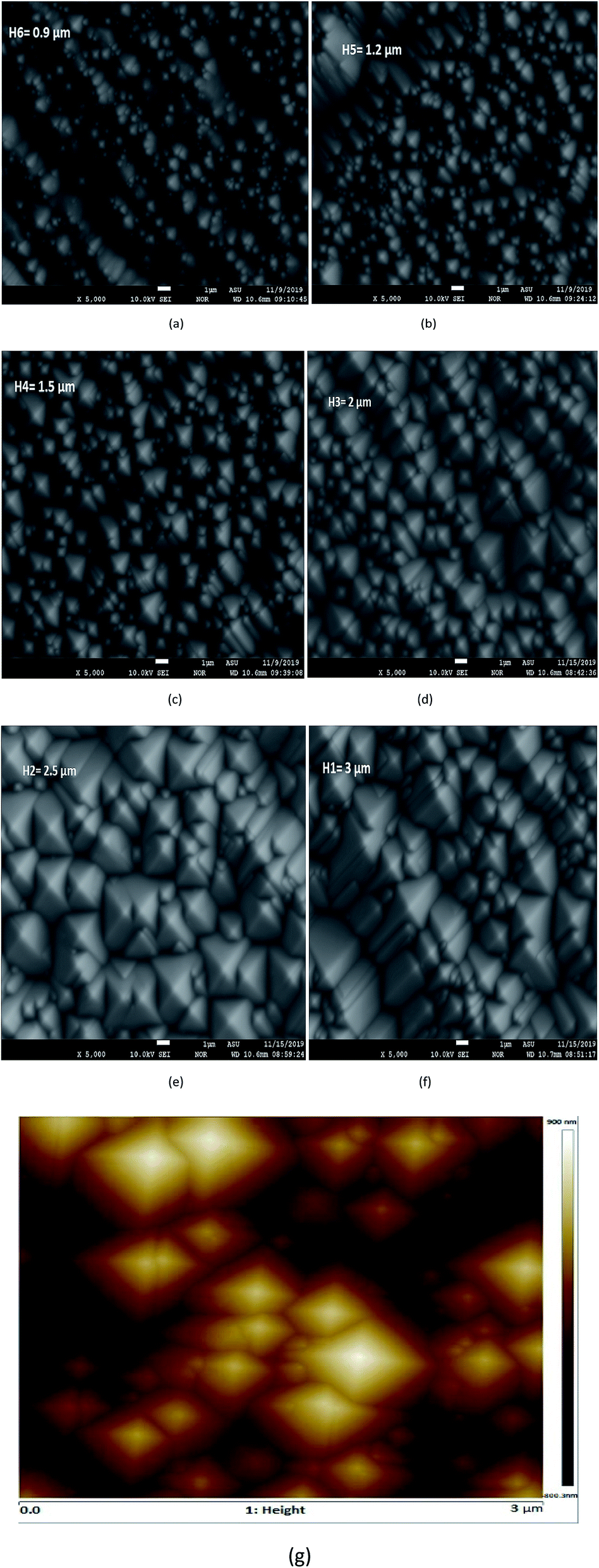 | ||
| Fig. 1 (a–f) SEM images of the textured silicon sample to analyze the surface topography of different pyramid heights under 5000 resolution, and (g) AFM image of textured silicon. | ||
For evaluating the optical response of the textured silicon sample, we used an ARTA and a spectrophotometer. Fig. 2(a) shows the angular reflectance of the textured sample obtained at different pyramid heights ranging from 3 to 0.9 μm size. These ARTA results were obtained from an angle in the range of −90 to 90 degree for an entire front surface coverage. The results indicated that H1 of 3 μm was not a suitable option for solar cell applications because it supports a maximum reflection of 0.91 at −24° with a base angle of 51°. Similarly, the H2, H3 and H4 heights were not good options because they exhibited maximum reflection peaks. The height H6 appeared to provide very low reflection; however, at large angles, the reflection gradually maximized. Therefore, the height H5 of 1.2 μm was comparatively suitable in our case. Moreover, the scattering effect, which is significant for light trapping, usually comes into picture when the pyramid height is equal or closer to silicon bandgap energy.32 In our case, the scattering effect is only supported by heights H5 and H6 at a wavelength in the range of 400–800 nm, as shown in Fig. 2(b). Therefore, we have chosen a pyramid height between 0.9 and 1.2 μm for our further analyses of perovskite/silicon tandem development in the simulation environment.
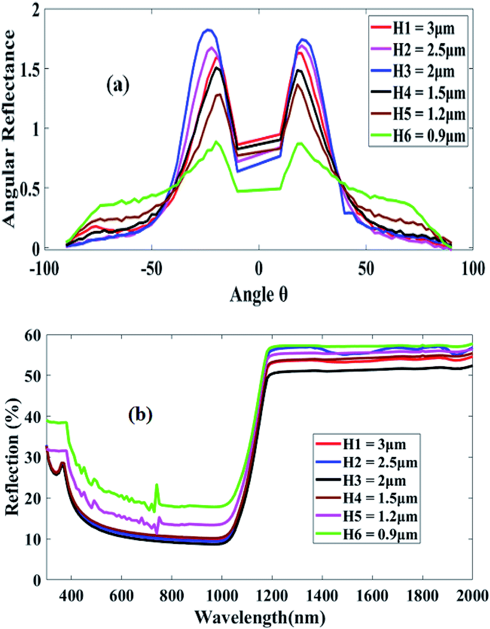 | ||
| Fig. 2 (a) Angular resolved reflectance of textured c-Si with different pyramid heights, and (b) reflectance of textured c-Si with different pyramid heights (extracted from AFM). | ||
Optical simulations
We used the optimum pyramid height of the silicon sample and deposited a wide bandgap perovskite material on top of it. In this way, we made a complete perovskite/silicon tandem solar cell with all functional layers, as shown in Fig. 3. The description of each layer is as follows: MgF2 acted as an anti-reflective coating layer, which is responsible for minimizing the reflection losses from the top surface;33 indium tin oxide (ITO) was used as a transparent conductive oxide for the front contact; tin oxide (SnO2) was used as a buffer layer; buckminsterfullerene (C60) was used as an electron transport layer; the wide band gap perovskite was used as an absorber for the top subcell; nickel oxide (NiO) was used as a hole-selective layer followed by an interconnecting ITO layer; the bottom subcell contained textured silicon heterojunction (HJ), consisting of n+ doped and intrinsic (i) hydrogenated amorphous silicon (a-Si:H) layers, the textured c-Si wafer; i and p+ doped a-Si:H layers and the textured silver (Ag) back reflector and contact. The simulations are performed using the Sun Solve software from the PV lighthouse. Sun Solve is an effective tool, which gives optical information about each layer by combining Monte-Carlo-based ray tracing and thin-film optics.34 The optical constants for perovskites and all other layers including MgF2, crystalline silicon, silver, intrinsic and doped (n- and p-type) amorphous silicon (a-Si:H), the intermediate ITO layer, and the rear ITO layer were taken from the literature.6,35–39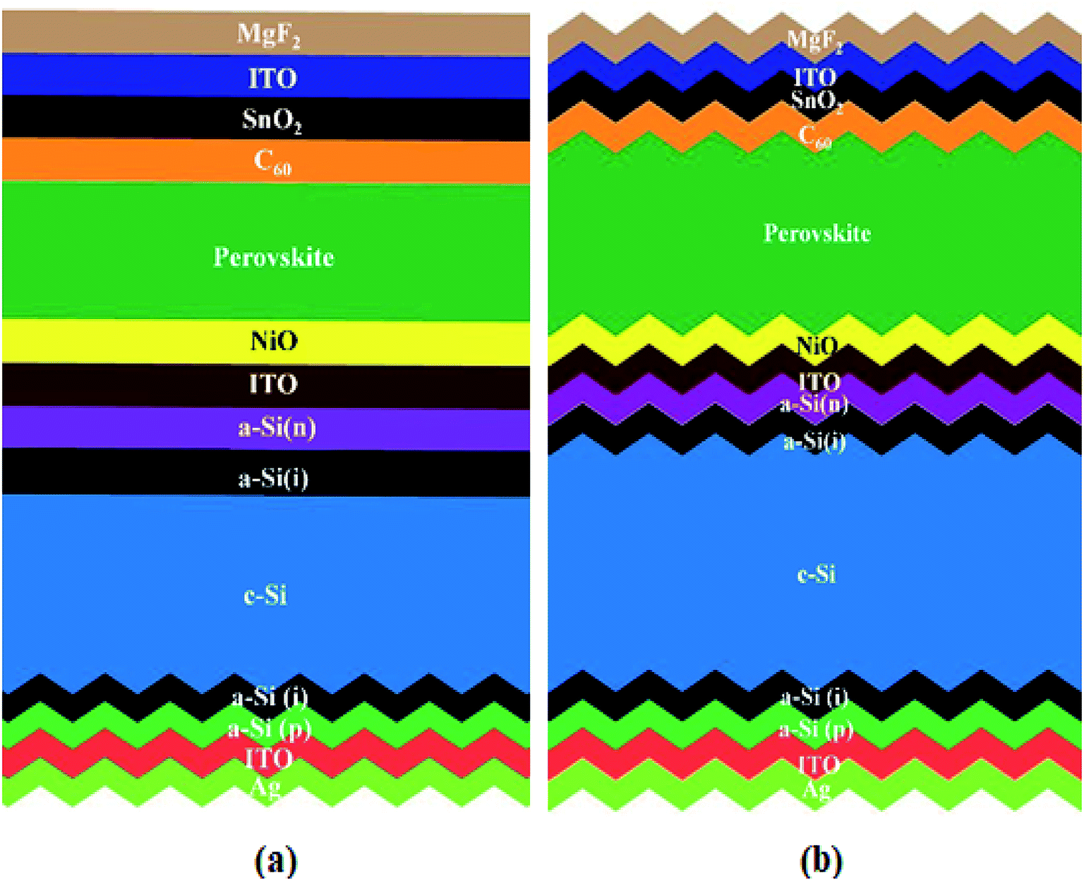 | ||
| Fig. 3 Perovskite/silicon tandem solar cells with (a) front side polished and (b) double sides textured. | ||
As discussed, for analysis, we have considered two different kinds of wide bandgap perovskite materials such as Cs17/Br17 having a bandgap of 1.63 eV and Cs25/Br20 having a bandgap 1.67 eV, respectively. The thicknesses of each layer of both kinds of perovskites (Cs17/Br17, Cs25/Br20) in a tandem configuration were optimized, which are displayed in Table 1. The optimization is performed by matching currents between perovskite and silicon subcells. Thus, in this way, a thickness of 500 nm was obtained for Cs17/Br17 and 650 nm for Cs25/Br20, and all other thicknesses remained constant. Moreover, the short-circuit current density (Jsc) was evaluated by taking integration of the product of the absorption spectrum as a function of wavelength under AM1.5G spectral irradiance over the wavelength range of 300–800 nm for Cs17/Br17, while the spectral range was 300–760 nm for Cs25/Br20. Table 2 indicates the thickness and corresponding current density values of each layer in a tandem configuration. A perfect match was obtained between the current density of perovskites and silicon subcells.
| Layer | Perovskite Cs17/Br17 thickness (nm) | Perovskite Cs25/Br20 thickness (nm) |
|---|---|---|
| Front ITO | 120 | 120 |
| SnO2 | 15 | 15 |
| C60 | 15 | 15 |
| Perovskite | 500 | 650 |
| NiOx | 20 | 20 |
| Rear ITO | 20 | 20 |
| Glass | 1000 | 1000 |
| Ag | 300 | 300 |
| Layer | Perovskite/silicon tandem layer thickness (nm) | Jsc (mA cm−2) |
|---|---|---|
| MgF2 | 100 | 0.065 |
| ITO front | 120 | 1.653 |
| SnO2 | 15 | 0.256 |
| C60 | 15 | 1.214 |
| Perovskite (Cs17/Br17/Cs25/Br20) | 500/650 | 20.34 |
| NiOx | 20 | 0.325 |
| Intermediate ITO | 20 | 0.418 |
| a-Si:H(n) | 8 | 0.005 |
| a-Si:H(i) | 8 | 0.002 |
| c-Si | 250![[thin space (1/6-em)]](https://www.rsc.org/images/entities/char_2009.gif) 000 000 |
20.09 |
| a-Si:H(i) | 8 | 0.000 |
| a-Si:H(p) | 11 | 0.000 |
| Rear ITO | 180 | 0.431 |
| Ag | 300 | 0.225 |
In order to analyze the performance of the two types of tandem cells (Cs17/Br17–Si, and Cs25/Br20–Si), we have simulated the cells with flat and textured top perovskite subcells. It has to be noted that the bottom silicon subcell is textured in both kinds of tandem cells. Fig. 4(a) shows the absorption and reflectance spectra of a Cs17/Br17–Si tandem configuration with flat perovskite top subcells. It appears that the reflectance indicated by the gray curve is relatively large at long wavelengths, which essentially reduces the current density in this spectral region. Moreover, the current mismatching was high in this case; perovskite exhibited 20.34 mA cm−2, while silicon supported 18.44 mA cm−2. This current mismatch between the cells will lead to low efficiency and eventually reduce the life time of the cell. In Fig. 4(b), the absorption and reflectance spectra were calculated for the double-side-textured surface. In this case, the absorption in the long wavelength region is significantly improved due to scattering effect induced by the textured surfaces. The difference in the current density values reduced from 1.86 mA cm−2 (flat perovskite) to 0.25 mA cm−2, which is quite acceptable in tandem configuration.26 Fig. 4(c) shows the absorption and reflectance spectra of a Cs25/Br20–Si tandem configuration with flat perovskite top subcells. The absorption characteristics in this case slightly changed compared to the previous case. Herein, the current mismatch was 1.65 mA cm−2, which was somewhat lower than that of the previous case. However, by introducing double-side texturing (Fig. 4(d)), the difference in the current matching appears the same as calculated in Fig. 4(b). Furthermore, the tandem models were tested with planar and double-side-textured silicon surfaces, and it was found that the planar structure limits the photocurrent value to ∼18.44 mA cm−2, a value that is ∼2 mA cm−2 lesser in comparison to a double-side-optimized texture design. Finally, in order to show which of the tandem configurations is better, we calculated the photovoltaic parameters including short current density (Jsc), open circuit voltage (Voc), fill factor (FF), and efficiency (η), as shown in Table 3. It becomes clear that the tandem cell of type Cs25/Br20–Si is the best option because of improved photovoltaic parameters compared to Cs17/Br17–Si. The highest conversion efficiency obtained was about 28.20%, which indicated that the proposed cell may be used for commercial applications.
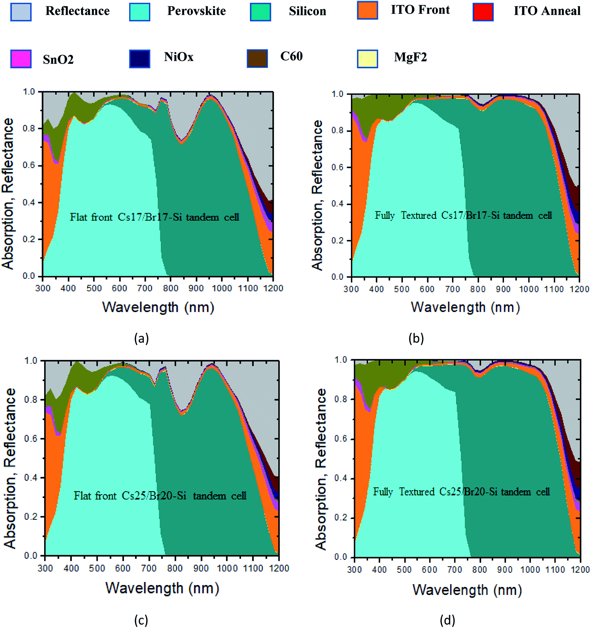 | ||
| Fig. 4 Absorption and reflectance spectra of perovskite/Si tandem solar cells with (a) front-side-polished Cs17/Br17–Si, (b) double-side-textured Cs17/Br17–Si, (c) front-side-polished Cs25/Br20–Si, and (d) double-side-textured Cs25/Br20–Si, respectively. | ||
| Perovskite–silicon tandem cell | Voc (V) | Jsc (mA cm−2) | FF (%) | η (%) |
|---|---|---|---|---|
| Cs17/Br17–Si | 1.72 | 20.09 | 77.43 | 26.75 |
| Cs25/Br20–Si | 1.78 | 20.09 | 79.01 | 28.20 |
We finally compared the proposed efficient tandem solar cell with the existing tandem structures, as shown in Table 4. Our cell supports relatively large values of Voc, Jsc, FF, and η, respectively, which indicates that it can be used for practical applications.
| Reference | Structure | Voc (V) | Jsc (mA cm−2) | FF (%) | η (%) |
|---|---|---|---|---|---|
| 24 | Monolithic single side textured perovskite–c-Si HJ | 1.75 | 16.89 | 74.30 | 21.93 |
| 25 | Monolithic planar perovskite–c-Si HJ | 1.69 | 18.04 | 75.43 | 23.08 |
| 30 | Monolithic fully textured perovskite–c-Si HJ | 1.78 | 19.5 | 73.10 | 25.20 |
| 26 | Monolithic planar perovskite–c-Si HJ | 1.76 | 19.2 | 76.50 | 26.00 |
| 17 | 4-Terminal planar perovskite–c-Si HJ | — | — | — | 27.0 |
| 31 | Monolithic fully textured perovskite–c-Si HJ | 1.82 | 19.3 | 74.4 | 26.0 |
| Current study | Proposed monolithic perovskite–c-Si HJ | 1.78 | 20.09 | 79.01 | 28.20 |
Conclusion
In summary, an experimental investigation has been performed to optimize the pyramid height of the textured silicon cell to improve light trapping in solar cells. Two different perovskite materials such as Cs0.17FA0.6Pb(Br0.17I0.7)3 and Cs0.25FA0.6Pb(Br0.20I0.7)3 with wide bandgaps have been deposited on the optimized textured silicon cell to form a tandem solar cell with all essential functional layers. To evaluate the performance of the proposed tandem cells, a comparison has been made between flat and fully textured surfaces. In case of the flat surface tandem solar cell, the current mismatch between the top and bottom subcells was quite high (1.86 mA cm−2) compared to the fully textured tandem solar cell (0.25 mA cm−2). Moreover, improved absorption efficiencies and less reflection losses have been obtained in case of the textured tandem solar cell compared to the flat cell. Finally, the photovoltaic parameters of our cell have been compared to existing solar cells, and it has been found that our proposed cell appears to support high values of Voc = 1.78 V, Jsc = 20.09 mA cm−2, FF = 79.01%, and η = 28.20%, which indicates that our design could be a better option for the photovoltaic community.Conflicts of interest
There are no conflicts of declare.References
- C. Battaglia, A. Cuevas and S. De Wolf, Energy Environ. Sci., 2016, 9, 1552–1576 RSC.
- National Renewable Energy Laboratory (NREL), https://www.nrel.gov/pv/cell-efficiency.html, accessed 1st December 2019.
- K. Yoshikawa, W. Yoshida, T. Irie, H. Kawasaki, K. Konishi, H. Ishibashi, T. Asatani, D. Adachi, M. Kanematsu and H. Uzu, Sol. Energy Mater. Sol. Cells, 2017, 173, 37–42 CrossRef CAS.
- A. Richter, M. Hermle and S. W. Glunz, IEEE J. Photovolt., 2013, 3, 1184–1191 Search PubMed.
- S. Essig, C. Allebé, T. Remo, J. F. Geisz, M. A. Steiner, K. Horowitz, L. Barraud, J. S. Ward, M. Schnabel and A. Descoeudres, Nat. Energy, 2017, 2, 17144 CrossRef CAS.
- S. Manzoor, J. Häusele, K. A. Bush, A. F. Palmstrom, J. Carpenter, J. Y. Zhengshan, S. F. Bent, M. D. Mcgehee and Z. C. Holman, Opt. Express, 2018, 26, 27441–27460 CrossRef CAS PubMed.
- F. Hou, C. Han, O. Isabella, L. Yan, B. Shi, J. Chen, S. An, Z. Zhou, W. Huang and H. Ren, Nano energy, 2019, 56, 234–240 CrossRef CAS.
- Z. J. Yu, M. Leilaeioun and Z. Holman, Nat. Energy, 2016, 1, 1–4 Search PubMed.
- M. Abdi-Jalebi, Z. Andaji-Garmaroudi, S. Cacovich, C. Stavrakas, B. Philippe, J. M. Richter, M. Alsari, E. P. Booker, E. M. Hutter and A. J. Pearson, Nature, 2018, 555, 497 CrossRef CAS PubMed.
- W. S. Yang, J. H. Noh, N. J. Jeon, Y. C. Kim, S. Ryu, J. Seo and S. I. Seok, Science, 2015, 348, 1234–1237 CrossRef CAS PubMed.
- S. De Wolf, J. Holovsky, S.-J. Moon, P. Löper, B. Niesen, M. Ledinsky, F.-J. Haug, J.-H. Yum and C. Ballif, J. Phys. Chem. Lett., 2014, 5, 1035–1039 CrossRef CAS PubMed.
- A. D. Khan, F. E. Subhan, A. D. Khan, S. D. Khan, M. S. Ahmad, M. S. Rehan and M. Noman, Optik, 2020, 164573 Search PubMed.
- J. Werner, B. Niesen and C. Ballif, Adv. Mater. Interfaces, 2018, 5, 1700731 CrossRef.
- D. Grant, K. Catchpole, K. Weber and T. White, Opt. Express, 2016, 24, A1454–A1470 CrossRef CAS PubMed.
- C. O. R. Quiroz, Y. Shen, M. Salvador, K. Forberich, N. Schrenker, G. D. Spyropoulos, T. Heumüller, B. Wilkinson, T. Kirchartz and E. Spiecker, J. Mater. Chem. A, 2018, 6, 3583–3592 RSC.
- A. Rohatgi, K. Zhu, J. Tong, D. H. Kim, E. Reichmanis, B. Rounsaville, V. Prakash and Y.-W. Ok, IEEE J. Photovolt., 2020, 10, 417–422 Search PubMed.
- Z. Wang, X. Zhu, S. Zuo, M. Chen, C. Zhang, C. Wang, X. Ren, Z. Yang, Z. Liu and X. Xu, Adv. Funct. Mater., 2020, 30, 1908298 CrossRef CAS.
- T. Todorov, O. Gunawan and S. Guha, Mol. Syst. Des. Eng., 2016, 1, 370–376 RSC.
- K. Jäger, L. Korte, B. Rech and S. Albrecht, Opt. Express, 2017, 25, A473–A482 CrossRef PubMed.
- M. Jošt, E. Köhnen, A. B. Morales-Vilches, B. Lipovšek, K. Jäger, B. Macco, A. Al-Ashouri, J. Krč, L. Korte and B. Rech, Energy Environ. Sci., 2018, 11, 3511–3523 RSC.
- P. Campbell, J. Opt. Soc. Am. B, 1993, 10, 2410–2415 CrossRef CAS.
- D. L. King and M. E. Buck, Experimental optimization of an anisotropic etching process for random texturization of silicon solar cells, Sandia National Labs., Albuquerque, NM (United States), 1991 Search PubMed.
- B. W. Schneider, N. N. Lal, S. Baker-Finch and T. P. White, Opt. Express, 2014, 22, A1422–A1430 CrossRef CAS PubMed.
- R. Pandey, A. Singla, J. Madan, R. Sharma and R. Chaujar, J. Micromech. Microeng., 2019, 29, 064001 CrossRef CAS.
- K. A. Bush, A. F. Palmstrom, J. Y. Zhengshan, M. Boccard, R. Cheacharoen, J. P. Mailoa, D. P. McMeekin, R. L. Hoye, C. D. Bailie and T. Leijtens, Nat. Energy, 2017, 2, 17009 CrossRef CAS.
- E. Köhnen, M. Jošt, A. B. Morales-Vilches, P. Tockhorn, A. Al-Ashouri, B. Macco, L. Kegelmann, L. Korte, B. Rech and R. Schlatmann, Sustainable Energy Fuels, 2019, 3, 1995–2005 RSC.
- K. A. Bush, K. Frohna, R. Prasanna, R. E. Beal, T. Leijtens, S. A. Swifter and M. D. McGehee, ACS Energy Lett., 2018, 3, 428–435 CrossRef CAS.
- Z. C. Holman, M. Filipič, A. Descoeudres, S. De Wolf, F. Smole, M. Topič and C. Ballif, J. Appl. Phys., 2013, 113, 013107 CrossRef.
- F.-J. Haug, M. Bräuninger and C. Ballif, Opt. Express, 2017, 25, A14–A22 CrossRef PubMed.
- F. Sahli, J. Werner, B. A. Kamino, M. Bräuninger, R. Monnard, B. Paviet-Salomon, L. Barraud, L. Ding, J. J. D. Leon and D. Sacchetto, Nat. Mater., 2018, 17, 820 CrossRef CAS PubMed.
- B. Chen, J. Y. Zhengshan, S. Manzoor, S. Wang, W. Weigand, Z. Yu, G. Yang, Z. Ni, X. Dai and Z. C. Holman, Joule, 2020, 4, 850–864 CrossRef CAS.
- S. Manzoor, Light trapping in monocrystalline silicon solar cells using random upright pyramids, Arizona State University, 2014, ISBN-1321121393 Search PubMed.
- C. Zhao, C. Ma, J. Liu, Z. Liu and Y. Chen, Mater. Res. Express, 2020, 7, 026415 CrossRef.
- D. Payne, M. Abbott, A. C. Lopez, Y. Zeng, T. H. Fung, K. McIntosh, J. Cruz-Campa, R. Davidson, M. Plakhotnyuk and D. Bagnall, Proceedings of the 33rd European Photovoltaic Solar Energy Conference and Exhibition (EUPVSEC), 2017 Search PubMed.
- Y. Jiang, S. Pillai and M. A. Green, Sci. Rep., 2016, 6, 30605 CrossRef CAS PubMed.
- M. Leilaeioun, J. Y. Zhengshan and Z. Holman, IEEE 43rd Photovoltaic Specialists Conference (PVSC), 2016, pp. 0681–0684 Search PubMed.
- H. T. Nguyen, F. E. Rougieux, B. Mitchell and D. Macdonald, J. Appl. Phys., 2014, 115, 043710 CrossRef.
- J. M. Siqueiros, R. Machorro and L. E. Regalado, Appl. Opt., 1988, 27, 2549–2553 CrossRef CAS PubMed.
- S. Manzoor, M. Filipič, M. Topič and Z. Holman, IEEE 43rd Photovoltaic Specialists Conference (PVSC), 2016, pp. 2952–2954 Search PubMed.
| This journal is © The Royal Society of Chemistry 2020 |