DOI:
10.1039/D0RA04424E
(Paper)
RSC Adv., 2020,
10, 25170-25176
Two-dimensional aluminum phosphide semiconductor with tunable direct band gap for nanoelectric applications†
Received
18th May 2020
, Accepted 23rd June 2020
First published on 2nd July 2020
Abstract
More and more attractive applications of two-dimensional (2D) materials in nanoelectronic devices are being achieved successfully, which promotes the rapid and extensive development of new 2D materials. In this work, the structural and electronic properties of the V structure aluminum phosphide (V-AlP) monolayer are examined by density functional calculations, and its electronic properties under strain and an electric field are also explored in detail. The computation results indicate that it has good stability. Interestingly, it possesses a wide direct gap (2.6 eV), and its band gap exhibits a rich behavior depending on the strain, E-field and layer stacking. Under biaxial strain, its band gap can be tuned from 1 eV to 2.6 eV. And a direct-indirect band gap transition is found when external tension is applied. The V-AlP monolayer also exhibits anisotropic behavior as its band structure variation trends under strains along different directions are obviously different. When the external E-field is changed from 0.5 V Å−1 to 1 V Å−1, the band gap of the V-AlP monolayer can be tuned linearly from 0 eV to 2.6 eV. Layer stacking narrows the band gap of the 2D V-AlP material. It is concluded that strain, E-field and layer stacking can all be used effectively to modify the electronic property of the V-AlP monolayer. Thus, these results indicate that the V-AlP monolayer will have promising applications in nanoelectric devices.
Introduction
The discovery of graphene opens up a great window for the development of 2D materials, and furthermore the vast development of 2D materials has attracted much attention because of their excellent and abundant physical properties with potential applications in a wide range of fields.1–3 Usually the pristine 2D material has a limitation in application, for example the zero band gap of graphene limited its application in nanoelectronic devices.4–6 Therefore, to make full use of these 2D materials, many chemical and physical methods are used to tune their properties, such as chemical modification, applying strain and electric field, etc.7–12 For example, the band gap for graphene can be opened by applying an external strain.7
AlP is a typical III–V compound below BN in the periodic table, which is a wide band-gap semiconductor.13,14 To date, the research reports on AlP are by far less than those of BN. AlP in bulk form has several important applications, such as photo-detectors, light emitting diodes and spintronics owing to its excellent electronic and magnetic properties.15–19 In previous works, atom doping is used to change the physical properties of AlP, and many novel electronic and magnetic properties are found, which satisfying the requirement of new nanoelectric devices.17–22
AlP exhibits zinc blende structure at normal conditions with an experimental lattice constant of 5.463 Å,23 which is very approaching to that of silicon crystals. Meanwhile, the sheets of silicene have been achieved recently in experiments with epitaxial growth of silicon on Ag(111).24 This naturally motivates us to ask whether exist any AlP monolayer or nanostructure as isoelectronic counterpart of silicene and what new physical properties they will exhibit. It's our pleasure to find that a few researchers have tried to answer the above scientific problems and have partly solved the problem.25–27 For example, Sun et al. reported the stability and electronic structures of single-walled AlP nanotubes by theoretically calculations.25 They found that AlP zigzag nanotubes are direct band gap semiconductor and therefore have great potential in applications as solar photovoltaic devices. Through cleaving and optimizing from zinc blende bulk lattice, Tong et al. theoretically obtained 27 2D single-layer structures of zinc-blende compounds, which include two type of 2D AlP structures (Tetragonal structure and V structure AlP) with versatile electronic and optical properties.26 Recently, Liu et al. researched the 2D tetragonal AlP (T-AlP) monolayer based on density functional theory, and found that the band gap feature of the T-AlP monolayer can be modulated by the strain and layer stacking order.27
In this work, an in-depth study on the structural, electronic properties of the V-AlP monolayer by density functional calculations are done. Based on the structure optimization and phonon spectrum calculations, it was found that the V-AlP monolayer is also stable. The electronic property of V-AlP monolayer is studied and a wide direct band gap of 2.6 eV is found. The absorption spectrum of V-AlP monolayer is also studied and it shows a strong light harvesting ability in the ultra-violet range of the solar spectrum. In the next step, the influences of external strain and electric field on V-AlP monolayer are explored in detail. It's found that the V-AlP monolayer have a wide and tunable direct band gap with the strain and E-field. The electronic band structure of V-AlP monolayer can be suddenly changed from a direct band gap to an indirect one, and it also can be tuned between semiconductor and metal. Interestingly, the anisotropic property of V-AlP monolayer under strains is also observed. At last, the influences of layer stacking on the electronic properties of V-AlP monolayer is studied. Our calculation results indicate that it can become a promising candidate in nanoelectric devices.
Computational method
All the structures were optimized before calculation. The electronic structures were employed in CASTEP package by using density functional theory.28 The Perdew–Burke–Ernzerhof (PBE) functional and the Heyd–Scuseria–Ernzerhof (HSE) hybrid functional are used.29–32 For the HSE06 functional, the used screening parameter is 0.21/Å and the mixing parameter for the short-range exchange is 0.25 respectively. A vacuum region greater than 20 Å perpendicular to the sheets (along the c-axis) is applied to avoid interactions between the layers caused by the periodic boundary condition. We perform van der Waals (vdW) calculations based on the Tkatchenko and Scheffler approaches, considering the dispersion interaction between layers.33 The basis set of valence electronic states is set to be 3 s2 3p1 for Al and 3s2p3 for P respectively. For the geometry optimization and electronic properties calculations, a kinetic-energy cutoff for the plane-wave expansion is set to 500 eV. The atomic structure is relaxed until all residual force on each atom is smaller than 0.01 eV Å−1. The total energy tolerance is below 10−6 eV, and the maximum stress is 0.02 eV Å−1. We also use a 15 × 15 × 1 Monkhorst–Pack-points grid to sample the 2D Brillouin zone for the structural optimization and band calculations.29 The cohesive energy is defined as Ecoh = ETot/N − γiEi, where ETot and Ei are the total energy of the system and the energy of a single atom, respectively. N is the number of atoms of the unit cell. γi is the ratio of the number of atoms of the ith atom in the unit cell to the total number of atoms.
Results and discussions
Geometric structure and stability
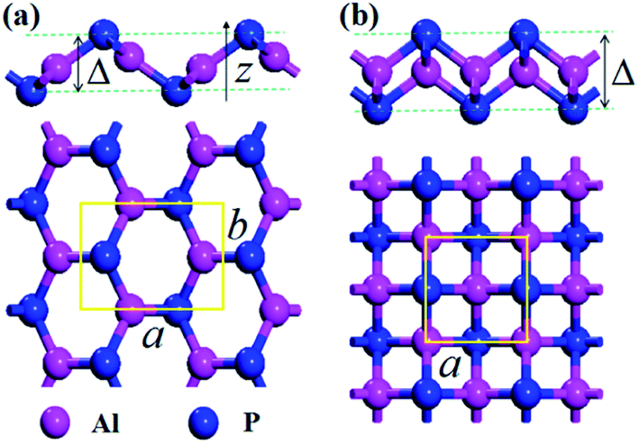
The crystal structures of the AlP monolayer unit cells (T-AlP and V-AlP monolayer) after full relaxations are shown in Fig. 1. The lattice parameters, bond lengths and thickness of the AlP monolayers are listed in Table 1. The V-AlP monolayer in Fig. 1(a) belongs to the space group Pmn21,26 which has inequilateral hexagonal rings from the top view and a large buckle in the vertical direction. The bond lengths of the Al (P) atom with three adjacent P (Al) atoms are not the same, the bond length along lattice (a) direction is shorter (2.29 Å), while the other bond length is longer (2.32 Å). And as shown in Fig. 1(b), the tetragonal structure of T-AlP belongs to the space group P4/nmm. It is a layered structure with an Al atom layer sandwiched between two P atom layers. Each Al (P) atom is surrounded by other four P (Al) atoms. It's found that the mean bond length of V-AlP (2.31 Å) is 4.9% shorter than that of T-AlP (2.43 Å),27 therefore the V-AlP monolayer is more strong. The thickness of the two types AlP monolayers are different (the thickness values are listed in Table 1), and the thickness of V-AlP monolayer is 23.4% thinner than that of the T-AlP monolayer. It's found from Table 1 that our calculation results (the lattice parameters, bond length and thickness of T-AlP monolayer) are in excellent agreement with previous literatures,26,27 therefore, our calculation methods are effective and the crystal models we obtained are valid.
 |
| | Fig. 1 Optimized structures of V-AlP (a) and T-AlP (b) monolayers with the unit cells. The thicknesses are labeled by symbol Δ and the primitive cells of the corresponding structure are marked by yellow rectangular. The bright red and blue balls represent Al and P atoms respectively. | |
Table 1 The lattice parameter (a and b), bond lengths (l), thickness (Δ), cohesive energy (Ecoh) and (Eg) of the AlP monolayers. The thickness is defined by the vertical distance between upper and lower layer atoms in the monolayer. The units of energy and length are electron volts (eV) and angstroms (Å) respectively. The values in the parentheses correspond to the energy calculated by the HSE06 method. The data with a star symbol behind as a superscript is adopted from ref. 27
| Model |
a, b |
l |
Δ |
Ecoh |
Eg |
| T-AlP |
a = 3.91 |
2.43 |
2.87 |
−5.35 |
0.97 (1.54) |
| a = 3.90* |
2.42* |
2.86* |
−4.10* |
0.98 (1.56)* |
| V-AlP |
a = 5.68, b = 3.81 |
l1 = 2.29, l2 = 2.32 |
2.19 |
−5.12 |
1.74 (2.60) |
Stability is of vital importance for practical applications in theoretically designed 2D materials. In order to examine the kinetic stabilities of the two type AlP structures, the cohesive energies are calculated. The common negative value of cohesive energy of crystal indicates that such material has good kinetic stability. From the results in Table 1, it can be found that both the two type AlP monolayers have good stabilities (The cohesive energies of T-AlP and V-AlP are −5.35 eV and −5.12 eV, respectively). The stability of T-AlP are a little better than that of V-AlP. The negative cohesive energy of the single-layer blue phosphorene, which had been obtained by epitaxial growth, is −5.18 eV and almost equals to that of V-AlP monolayer.34 Therefore, V-AlP monolayer can be prepared in experimental preparation.
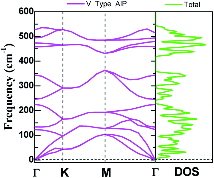
The dynamic stability of V-AlP monolayers can be inferred from the phonon dispersion calculation based on generalized gradient approximation functional (as shown in Fig. 2), where no apparent imaginary modes appear in the phonon spectrum for all wave vectors. Particularly, the highest frequency reaches up to 535 cm−1, which is higher than those of T-AlP (490 cm−1)27 and MoS2 monolayer (473 cm−1),35–37 indicating robust bonding between Al and P in the V-AlP monolayer. In the harmonic approximation, the positive frequencies of phonon modes and the elastic stability criteria are enough and necessary conditions for unstressed crystalline structures to be stable.38 The calculated elastic constants of V-AlP are C11 = 65.5 GPa, C12 = 8.4 GPa and C66 = 12.2 GPa, apparently satisfying the mechanical stability criteria (C11 > C12 and C66 > 0) for 2D V-AlP lattices.39
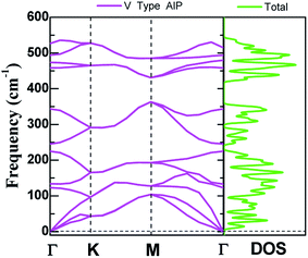 |
| | Fig. 2 The phonon spectra calculated with the primitive cell of V-AlP monolayer and corresponding density of states. | |
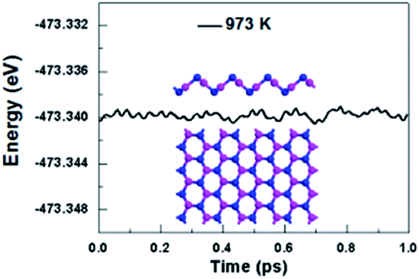
We further take into account the effect of the external temperature by performing ab initio molecular dynamics (MD) simulations. A larger initial atomic supercell (64 atoms) was used to increase the correlation length. The plane-wave basis set with a kinetic energy cutoff of 500 eV and norm-conserving pseudopotentials were used. This system was subjected to a heated condition of T = 973 K with a time step of 1 fs for the period of 1 ps, and the energy as function of MD simulation time is plotted in Fig. 3. And as shown in Fig. 3, the snapshot taken at the end of simulation is generally well-kept, showing V-AlP can be stable at the high temperature. Based on the above-mentioned situations, T-AlP and V-AlP monolayers could be experimentally synthesized in the near future. Next to the check of the stability of the V-AlP structure under high temperatures, we have performed ab initio MD to further verify the chemical stability of the structure in air at about room temperature. The V-AlP monolayer has been exposed to very high pressure gases (H2O, O2, N2 and H2) at temperatures T = 300 K. In our MD simulations, the number density of gas molecules was 7.13 × 1026 m−3. The V-AlP structure remains intact after 1 ps (Fig. S1†), indicating its chemical stability in air at the room temperature.
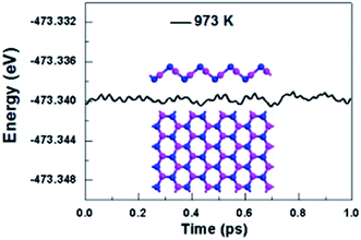 |
| | Fig. 3 The total energy of the supercell of V-AlP monolayer under 973 K as function of MD simulation time and the snapshot of the final frame at the end of 1 ps for the MD simulation at 973 K. | |
Electronic structures and optical properties
For 2D semiconductors applied in nano photoelectronic devices, the material with direct band gap is superior to that with indirect band gap. The photon absorption by electrons requires the participation of phonons in the indirect band gap semiconductor, therefore the photoelectric conversion effificiency of the device is limited. We calculated the band dispersions to gain insight into the electronic structure of V-AlP. Fig. 4 shows the band structure of V-AlP monolayer. As shown in Fig. 4(a), the direct band gaps of 1.74 eV and 2.60 eV are obtained at the PBE and HSE06 level, respectively. As shown in Fig. 4(b), the projected density of states (PDOS) of V-AlP presents that the p orbitals of P atoms contribute mainly to the valence band edge. In the energy range from −5 eV to −3 eV, the p orbitals of P are hybridized with the p orbitals of Al, resulting in the charge transfer from Al to P. The s and p orbitals of Al and p orbitals of P atoms are hybridized above the Fermi level to form conduction bands in the energy range from 2 eV to 4 eV. Especially, the p orbitals of Al and P actively contribute to the CBM. The nature of Al–P bonding can be illustrated based on the Hirshfeld charge and overlap population analyses. A small value of charge (0.21|e|) transfer from Al to P atoms together with the overlap population (0.105) of Al–P bonds reveals that V-AlP is combined by Al–P covalent bonds. The VBM and CBM at Γ-point are shown in Fig. 4(c), it can be found that the orbital hybridization in the V structure is neither sp2 nor sp,3 which is in agreement with ref. 26.
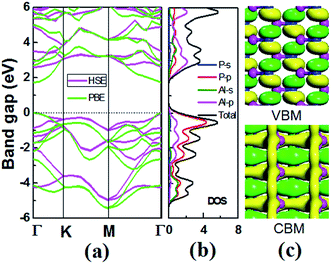 |
| | Fig. 4 (a) Band structures of monolayer V-AlP calculated at the PBE and HSE level. M, Γ and K are high-symmetry points in the first Brillouin zone. The Fermi energy is set to zero. (b) s- and p-orbital projected and total densities of states (electrons per eV). (c) Isosurfaces (0.05 e Å−3) of the conduction band minimum (CBM) and the valence band maximum (VBM) at the Γ-point. | |
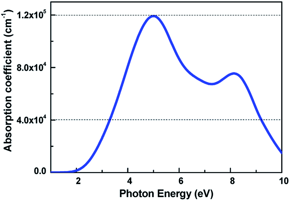
The light-absorbing performance of 2D V-AlP under light is investigated based on the adsorption coefficient. The light absorption spectra of the V-AlP nanosheet are calculated from the polarized light. As shown in Fig. 5, the prominent peaks of absorption coefficient are mainly located at about 5.00 eV and 8.14 eV respectively. In the photon energy range from 3.28 eV to 9.20 eV, the absorption coefficient is above one third of the magnitude of the first peak (4.0 × 104 cm−1), which implies that polarized light shows a strong light harvesting ability in the corresponding almost all ultra-violet range of the solar spectrum (378–134 nm). Therefore, V-AlP presents photoresponse of ultra-violet light, showing the potential applications in photoelectronic devices.
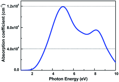 |
| | Fig. 5 Calculated absorption coefficient for V-AlP monolayer at the HSE06 level. | |
Strain and E-field effects
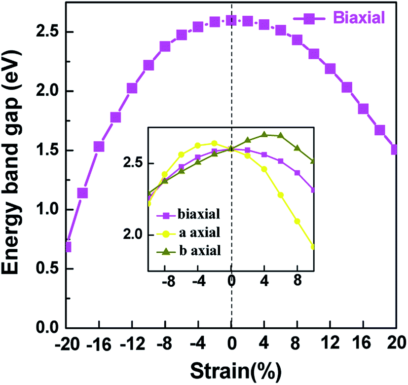
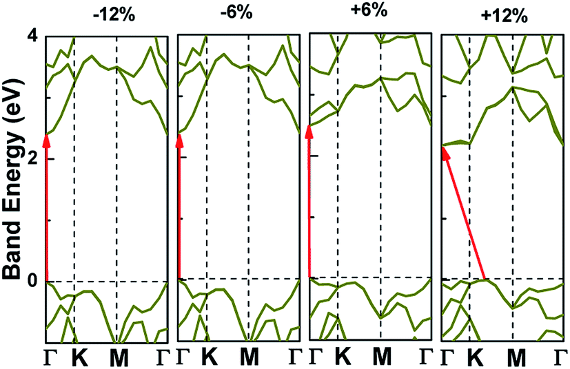
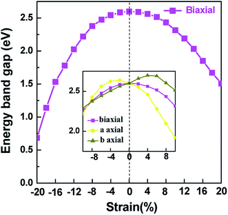
Applying external strain is known to be a promising mean to tune the energy gap of materials.9–12 Strain can be regarded as elastic field applied to the 2D materials, which usually changes the geometrical and electronic properties of materials. Under certain strain, the geometrical structure of material changes due to the interaction between the elastic field and 2D crystalline field, and then the electronic properties of materials change with the redistribution of electron density in 2D materials. However, the band structure of some typical 2D materials, such as graphene, is not sensitive to stress fields.7 Hence, we consider whether the applied stress is effective to tune the electronic property of V-AlP. In Fig. 6, under the axial strain applied along the lattice direction from −20% to +8%, the direct band-gap character of V-AlP is retained. The value of the direct band gap decreases with the increasing tension and compression. As the biaxial tension strain increases, the VBM moves from the Γ point to a near point, a direct–indirect band-gap transition occurs when the tension increase from +8% up to +10%. As shown in Fig. 7, the band-gap transition originates from the competition of the near-band-edge energy states. And the indirect band gap decrease monotonically up to +20% without any indirect–direct band gap transition. The tunable range of the direct band gap of V-AlP by means of biaxial strain at HSE level is from 1.0 eV to 2.6 eV, which is wide covering most of the visible sunlight energy range (from 1.6 eV to 3.1 eV). In the inset in Fig. 6, the change trends of the band-gap of V-AlP under mono-axial and biaxial strain from −10% to +10% are presented. It's obvious that these three variation curves of band gap value are different. The band gaps of V-AlP under different strains all increase monotonically at first and then decrease monotonically with the increase of strain from −10% to +10%, however, the inflection points (or extreme points) of the band-gap curves are different. The anisotropy of the strain effects on the V-AlP can be accounted for by the particular V structure, which also has its anisotropy property. The ideal band gap of solar cell materials is known to be 1.5 eV.40 The direct band gap of V-AlP monolayer may be tuned in a wide range (from 1.0 eV to 2.6 eV), therefore, it will have potential application in ultrathin photovoltaic materials. Our results hint that the electronic properties of the V-AlP monolayer are highly sensitive to the applied axial and biaxial strain. Therefore, the crucial variation in the band gap of V-AlP could lead to wide applications in designing flexible electronics and optoelectronic tunable photodetectors.
 |
| | Fig. 6 Changes in band gap with applied mono-axial and biaxial strain for V-AlP calculated by HSE06 functional. | |
 |
| | Fig. 7 Band structure change and the band edge shift under biaxial strains for V-AlP based on HSE functional. | |
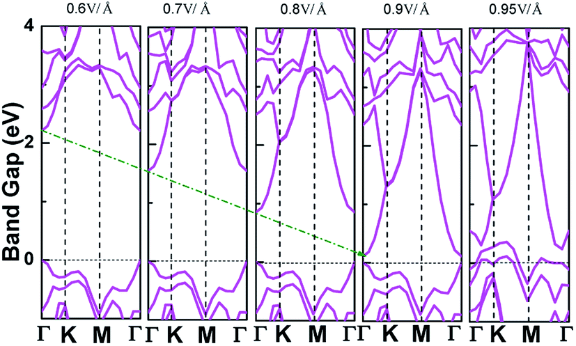
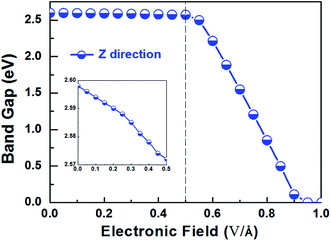
Applying external E-field is also a well-known effective method to tune the electronic properties of 2D materials.1,12 Thus, it is necessary to find the influence of E-field on the electronic properties of V-AlP, considering the direction perpendicular the to the V-AlP monolayer. The band gap of the V-AlP monolayer as a function of the external E-field is plotted in Fig. 8. Our results indicate that the changing trend of band gap highly relies on the intensity of external E-field. When the external E-field along the Z direction is below 0.5 V Å−1, the band gap first slightly and monotonically decreases, and when the external E-field is beyond 0.5 V Å−1, the band gap monotonically decreases rapidly. Moreover, metallic properties can also be observed when the intensity of E-field exceeds 0.90 V Å−1. As shown in Fig. 9, when the external E-field increases up to 0.95 V Å−1, the energy gap is closed, suggesting an essential change from semiconducting to metallic due to the up-shift of the VBM. Our study shows that the electric property of V-AlP monolayer can be tuned between direct band gap semiconductor and metal. Here, all these results can be accounted by the interaction between the built-in E-field and applied external E-field.12 That is to say, when the external E-field is applied, the total E-field is increased and the band gap is slowly decreased. Furthermore, when the total E-field reaches a certain value, the effect of external E-field is greatly increased, and then further increase of the external E-field strength can result in the rapidly decrease of the band gap. The variation of Hirshfeld charge transfer between the bonds in V-AlP monolayer under external E-field is also considered. When the external E-field is applied at the begin, the Hirshfeld charge transfer is unchanged (0.48|e| per pair of Al–P bonds). And when the E-field is beyond 0.5 V Å−1, the Hirshfeld charge transfer is changed (0.50|e| per pair of Al–P bonds), which means that the external E-field significantly influences the distribution of electron density resulting in rapidly decrease of the band gap. To further explore the mechanism of the change of band gap under external E-field, we studied the band edges under different external E-fields. Fig. 9 exhibits the band edges under certain external E-fields. It can be seen that the CBM of the V-AlP monolayer drops linearly with the increasing external E-field applied. Therefore, the decreasing band gap is mainly due to the down shift of the CBM. Fortunately, it's found that the V-AlP monolayer under the external E-field along z direction retain direct band gap, and the direct band gap can be tuned linearly by the external E-field in a wide range (from 0 eV to 2.6 eV). This large-scale band gap modulation indicates that applying E-field along z direction can offer an effectively dynamical control on the band structures and electronic properties in the V-AlP monolayer-based electronic nano-devices.
 |
| | Fig. 8 The band gap as a function of E-field along the Z direction perpendicular the plain of the V-AlP monolayer based on HSE functional. | |
 |
| | Fig. 9 The band structures of V-AlP monolayer under certain E-field along the Z direction. | |
Layer stacking effects
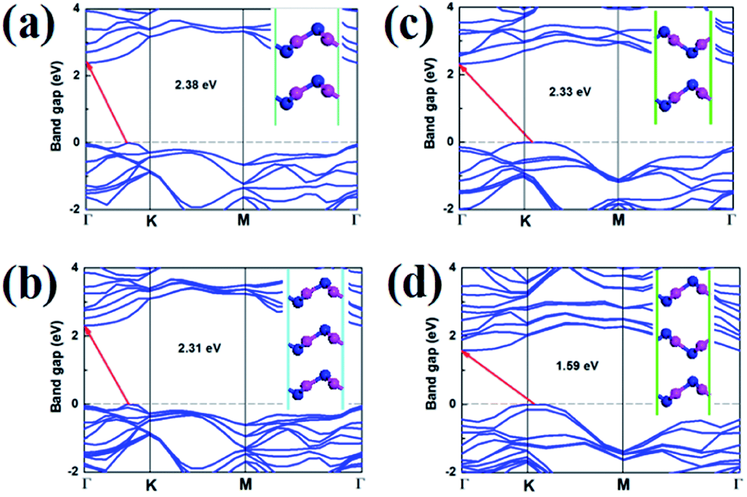
Stacking orders is also a effective method to tune the electronic properties of 2D materials.10,27 It is also interesting for us to research the influence of layer stacking order on the electronic properties of V-AlP. We optimized bilayer and trilayer V-AlP in AA, AB, AAA and ABA stacking orders. Two V-AlP monolayers are aligned without any rotation or displacement in the AA-stacking pattern. For AB-stacking conformation, the two layers shift along the lattice vector for a distance of half cell and P atom is just on top of the P atom. The obtained structural parameters including lattice constants and bond lengths differ slightly for different stacking pattern. The AA stacked bilayer is energetically favorable for the lower total energy, which is 16.7 meV per atom lower than that of AB one.
As shown in the Fig. 10, it is clear that the bilayer and trilayer V-AlP in AA, AB, AAA and ABA stacking orders are indirect semiconductors with narrower gaps of 2.38, 2.31, 2.33 and 1.59 eV, respectively. Therefore, stacking is obviously a effective method to tune the electronic properties of 2D V-AlP.
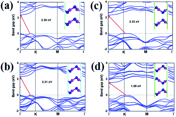 |
| | Fig. 10 Band structures (HSE) and geometries (inset) of V-AlP in (a) AA, (b) AB, (c) AAA and (d) ABA stacking orders. | |
Conclusion
In summary, based on the density functional theory calculation, we have systematically studied the geometrical property, stability and electronic band structure of the V-AlP monolayer. The V-AlP monolayer is thicker than the T-AlP monolayer. The good stability of V-AlP monolayer are proved by the calculation results of the negative binding energy, molecular dynamics simulation and phonon spectrum. Interestingly, it possesses a direct band gap with the value of 2.6 eV, which be helpful to nanoelectronic devices. The V-AlP monolayer shows a strong light harvesting ability in the ultra-violet range of the solar spectrum, therefore, it has potential applications in photoelectronic devices. And the band gap exhibits a fantastic behavior depending on the strain, external E-field and layer stacking. Under biaxial strain from −20% to 20%, the direct band-gap of V-AlP can be tuned from 1.0 eV to 2.6 eV. The band structure of the V-AlP monolayer exhibits anisotropic properties with strain along different direction. Besides, under external E-field along z direction from 0.5 V Å−1 to 1 V Å−1, the direct band-gap of V-AlP can also be tuned linearly in a wide range (from 0 eV to 2.6 eV). Therefore, it is concluded that the external E-field can be used effectively to modify the electronic property of the V-AlP monolayer. Through layer stacking, four bilayer and trilayer V-AlP are obtained and they are found to be indirect semiconductors with relatively narrower band gaps. The results pave the way for designing nanoelectric devices based on 2D V-AlP materials.
Conflicts of interest
The authors declare no competing financial interest.
Acknowledgements
This work was supported by the Natural Science Foundation of Xianning (XNKJ-28), the Scientific Research Project and Innovation Team of Hubei University of Science and Technology (HKCXTD-001; H2019003), the Natural Science Foundation of Jiangsu Province (BK20190741), the Natural Science Foundation of the Jiangsu Higher Education Institutions of China (19KJB140015), and the National scientific research project cultivation plan project and the Cultivate scientific research projects of Hubei University of Science and Technology (2020-22GP01; 2020-21X26).
References
- K. S. Novoselov, A. K. Geim, S. V. Morozov, D. Jiang, Y. Zhang, S. V. Dubonos, I. V. Grigorieva and A. A. Firsov, Science, 2004, 306, 666–669 CrossRef CAS PubMed.
- A. H. Castro Neto, F. Guinea, N. M. R. Peres, K. S. Novoselov and A. K. Geim, Rev. Mod. Phys., 2009, 81, 109–162 CrossRef CAS.
- S. Zhang, Z. Yan, Y. Li, Z. Chen and H. Zeng, Angew. Chem., Int. Ed., 2015, 54, 3112–3115 CrossRef CAS PubMed.
- S. Zhang, S. Guo, Z. Chen, Y. Wang, H. Gao, J. Gomez-Herrero, P. Ares, F. Zamora, Z. Zhu and H. Zeng, Chem. Soc. Rev., 2018, 47, 982–1021 RSC.
- T. Tan, X. Jiang, C. Wang, B. Yao and H. Zhang, Adv. Sci., 2020, 2000058 CrossRef PubMed.
- W. Zhou, S. Zhang, S. Guo, Y. Wang, J. Lu, X. Ming, Z. Li, H. Qu and H. Zeng, Phys. Rev. Appl., 2020, 13, 044066 CrossRef CAS.
- S. M. Choi, S. H. Jhi and Y. W. Son, Phys. Rev. B: Condens. Matter Mater. Phys., 2010, 81, 081407 CrossRef.
- W. Yu, C. Niu, Z. Zhu, X. Wang and W. Zhang, J. Mater. Chem. C, 2016, 4, 6581–6587 RSC.
- H. Qu, W. Zhou, S. Guo, Z. Li, Y. Wang and S. Zhang, Adv. Bioelectron. Mater., 2019, 1900813 CrossRef CAS.
- Y. Hu, C. Mao, Z. Yan, T. Shu, H. Ni, L. Xue and Y. Wu, RSC Adv., 2018, 8, 29862–29870 RSC.
- S. Zhang, Y. Hu, Z. Hu, B. Cai and H. Zeng, Appl. Phys. Lett., 2015, 107, 022102 CrossRef.
- C. Xia, J. Du, W. Xiong, Y. Jia, Z. Wei and J. Li, J. Mater. Chem. A, 2017, 5, 13400 RSC.
- H. Katayama-Yoshida and K. Sato, Physica B, 2003, 327, 337–343 CrossRef CAS.
- Y. Zhang, W. Liu and H. Niu, Solid State Commun., 2008, 145, 590–593 CrossRef CAS.
- Y. Saeed, A. Shaukat, S. Nazir, N. Ikram and H. A. Reshak, J. Solid State Chem., 2010, 183, 242–249 CrossRef CAS.
- Y. Zhang, J. Magn. Magn. Mater., 2013, 342, 35–37 CrossRef CAS.
- P. Liang, Y. Liu, X. Hu, L. Wang, Q. Dong and X. Jing, J. Magn. Magn. Mater., 2014, 355, 295–299 CrossRef CAS.
- M. Merabet, D. Rached, S. Benalia, A. H. Reshak, N. Bettahar, H. Righi, H. Baltache, F. Soyalp and M. Labair, Superlattices Microstruct., 2014, 65, 195–205 CrossRef CAS.
- Z. Yan, H. Wu and R. Zheng, Comput. Mater. Sci., 2015, 99, 16–20 CrossRef CAS.
- M. Boutaleb, B. Doumi, A. Tadjer and A. Sayede, J. Magn. Magn. Mater., 2016, 397, 132–138 CrossRef CAS.
- S. Wang, X. Fan and Y. An, Comput. Mater. Sci., 2018, 142, 338–345 CrossRef CAS.
- Y. Chen, Y. Xing, A. Jiang, C. Zhou and S. Lu, J. Magn. Magn. Mater., 2018, 457, 13–16 CrossRef CAS.
- H. Yu, K. Yao and Z. Liu, Solid State Commun., 2005, 135, 124–128 CrossRef.
- P. Vogt, P. De Padova, C. Quaresima, J. Avila, E. Frantzeskakis, M. C. Asensio and G. Le Lay, Phys. Rev. B: Condens. Matter Mater. Phys., 2012, 108, 155501 Search PubMed.
- J. Sun, Procedia Eng., 2011, 15, 5062–5066 CrossRef CAS.
- C. Tong, H. Zhang, Y. Zhang, H. Liu and L. Liu, J. Mater. Chem. A, 2014, 2, 17971–17978 RSC.
- S. Liu, Z. Teng, X. Ye and X. Yan, J. Mater. Chem. C, 2017, 5, 5999–6004 RSC.
- D. Vanderbilt, Phys. Rev. B: Condens. Matter Mater. Phys., 1990, 41, 7892–7895 CrossRef PubMed.
- J. P. Perdew and A. Zunger, Phys. Rev. B: Condens. Matter Mater. Phys., 1981, 23, 5048–5079 CrossRef CAS.
- J. P. Perdew, K. Burke and M. Ernzerhof, Phys. Rev. Lett., 1996, 77, 3865–3868 CrossRef CAS PubMed.
- J. Heyd, G. E. Scuseria and M. Ernzerhof, J. Chem. Phys., 2006, 124, 219906 CrossRef.
- H. J. Monkhorst and J. D. Pack, Phys. Rev. B: Solid State, 1976, 13, 5188–5192 CrossRef.
- A. Tkatchenko and M. Scheffler, Phys. Rev. Lett., 2009, 102, 073005 CrossRef PubMed.
- J. Zhang, S. Zhao, C. Han, Z. Wang, S. Zhong, S. Sun, R. Guo, X. Zhou, C. Gu, K. Yuan, Z. Li and W. Chen, Nano Lett., 2016, 16, 4903–4908 CrossRef CAS PubMed.
- S. Cahangirov, M. Topsakal, E. Aktürk, H. Şahin and S. Ciraci, Phys. Rev. Lett., 2009, 102, 236804 CrossRef CAS PubMed.
- A. Molina-Sanchez and L. Wirtz, Phys. Rev. B: Condens. Matter Mater. Phys., 2011, 84, 155413 CrossRef.
- L. Huang, P. Gong and Z. Zeng, Phys. Rev. B: Condens. Matter Mater. Phys., 2014, 90, 045409 CrossRef.
- G. Grimvall, B. Magyari-Köpe, V. Ozoliņš and K. A. Persson, Rev. Mod. Phys., 2012, 84, 945–986 CrossRef CAS.
- F. Mouhat and F. X. Coudert, Phys. Rev. B: Condens. Matter Mater. Phys., 2014, 90, 224104 CrossRef.
- M. C. Scharber, D. Mühlbacher, M. Koppe, P. Denk, C. Waldauf, A. J. Heeger and C. J. Brabec, Adv. Mater., 2006, 18, 789–794 CrossRef CAS.
Footnotes |
| † Electronic supplementary information (ESI) available: Ab initio MD snapshots of the V-AlP 3 × 3 supercell structures exposed to the high pressure (a) water vapour, (b) oxygen gas, (c) nitrogen gas and (d) hydrogen gas at temperatures T = 300 K. See DOI: 10.1039/d0ra04424e |
| ‡ These authors contribute equally. |
|
| This journal is © The Royal Society of Chemistry 2020 |
Click here to see how this site uses Cookies. View our privacy policy here. 
 Open Access Article
 This Open Access Article is licensed under a Creative Commons Attribution-Non Commercial 3.0 Unported Licence
 *a,
Hui Cao*b,
Yuping Zhanga,
Dong Zhaoa,
Zhiyuan Chena and
Meiqiu Xie*c
*a,
Hui Cao*b,
Yuping Zhanga,
Dong Zhaoa,
Zhiyuan Chena and
Meiqiu Xie*c