
 Open Access Article
 This Open Access Article is licensed under a
 Creative Commons Attribution 3.0 Unported Licence
Phase transition and thermal stability of epitaxial PtSe2 nanolayer on Pt(111)
Yongfeng Tonga,
Meryem Bouaziza,
Hamid Oughaddoubc,
Hanna Enriquezb,
Karine Chaouchia,
François Nicolasa,
Stefan Kubskya,
Vladimir Esaulovb and
Azzedine Bendounan *a
*a
aSynchrotron SOLEIL - L'Orme des Merisiers, Saint-Aubin - BP 48, 91192 Gif-sur-Yvette Cedex, France. E-mail: azzedine.bendounan@synchrotron-soleil.fr
bInstitut des Sciences Moléculaires d’Orsay, UMR 8214, Université Paris-Sud, Université Paris-Saclay, 91405 Orsay Cedex, France
cDépartement de Physique, Université de Cergy-Pontoise, 95031 Cergy-Pontoise Cedex, France
First published on 20th August 2020
Abstract
This work relates to direct synthesis of the two-dimensional (2D) transition metal dichalchogenide (TMD) PtSe2 using an original method based on chemical deposition during immersion of a Pt(111) surface into aqueous Na2Se solution. Annealing of the sample induces significant modifications in the structural and electronic properties of the resulting PtSe2 film. We report systematic investigations of temperature dependent phase transitions by combining synchrotron based high-resolution X-ray photoemission (XPS), low temperature scanning tunnelling microscopy (LT-STM) and low energy electron diffraction (LEED). From the STM images, a phase transition from TMD 2H-PtSe2 to Pt2Se alloy monolayer structure is observed, in agreement with the LEED patterns showing a transition from (4 × 4) to (√3 × √3)R30° and then to a (2 × 2) superstructure. This progressive evolution of the surface reconstruction has been monitored by XPS through systematic de-convolution of the Pt4f and Se3d core level peaks at different temperatures. The present work provides an alternative method for the large scale fabrication of 2D transition metal dichalchogenide films.
I. Introduction
Two-dimensional (2D) nano-materials have been extensively studied over the past decade and are now being considered as the next generation of materials for future high-technology applications. In particular, the rapid advances in graphene and silicene research1–5 have led to considerable interest in other types of 2D systems such as germanene, phosphorene, boron nitride and transition metal dichalchogenide (TMD) layers.6–10 In addition to chemical composition, atomic arrangement and dimension proved to be one of the most important parameters in determining film properties and device performance. 2D layer materials, especially in the monolayer limit, have aroused enormous attention because they exhibit interesting novel properties that are rather different from those of the bulk phase. Among the ideal candidates, TMDs have versatile physical and chemical properties that offer great potential for exploration in areas such as energy storage, nano-electronics and sensor technologies. The TMDs' family is described with the common formula MX2, where M stands for a transition metal (M = Mo, W, Nb, Ta, Ti) and X for the chalchogenide element, i.e. S, Se or Te. MX2 forms either the 1T- or 2H-structure (with the sub-X layers 180°- or 0°-rotated with respect to each other) without surface dangling bonds. The former is of a metallic character while the latter has a semiconductor nature. Depending on the metal and the chalcogen involved in the growth process; their electrical properties span the range from semiconducting to superconducting. For instance, phase transitions of 1T to 2H in 2D TMDs tend to occur at elevated temperatures or by simple lithiation.11 Many of the TMDs require chemical modifications to make them suitable for a wide variety of applications.In addition, MX2 can exhibit peculiar transitions like metal–insulator transition, or superconductivity at low temperature. The most studied TMDs are those based on S and Se atoms. These two chemical elements are also involved in functionalization activity of the so-called organic self-assembled monolayers (SAMs) where the chalcogen atom of the head group provides the bond with the metal substrate.12,13 Intensive effort has been dedicated to the study of sulfur interaction with Au, Ag and Cu surfaces, focusing on the formation of self-assembled monolayers and its behavior under various environments. These studies range from analyzing atomic S to molecules with chain structure (alkane) or aromatic molecule (thiols, dithiols, thiophene). The interaction between the S headgroup and metal surfaces plays an important role in determining the characteristics of the organic–metal hybrid system, including film structure, orientation, bond state. The layered MoS2, PtS2 are also the first 2D TMD materials that have been studied for their physical and chemical properties.14,15
Perhaps selenium (Se) has attracted less interest; it nevertheless has good photovoltaic and photoelectric properties, which explains why Se-based compounds are being successfully introduced in the fields of Lithium Ion Battery (LIB), solar cells, detectors and lasers.16–18 Attention has been paid to the Se-based TMD materials like MoSe2, WSe2 and recently PtSe2. In particular, a PtSe2 monolayer was epitaxially grown on a clean Pt(111) surface.19 Upon annealing at 250 °C, a (3 × 3) superstructure was observed by low energy electron diffraction (LEED). An octahedral structure was proposed according to the observation from the scanning transmission electron microscopy (STEM) image of the film cross section.19 The bulk PtSe2 is a semimetal with zero band gap,20,21 however the PtSe2 monolayer has a band gap of 1.2 eV confirming theoretical predictions to this effect.22–24 Previously, PtSe2 has been used as a photocatalytic material in graphene nano-composites.25 In addition, its potential for hybrid electronic devices has also been demonstrated through the example of a high-performance gas sensor and photo-detector, as well as a photovoltaic cell.26
The PtSe2 monolayers have been produced by vacuum evaporation of Se on a Pt (111) substrate or by what the authors of ref. 26 called thermally assisted conversion (TAC) in which a Pt thin film grown on a silicon substrate (Si/SiO2) was exposed to Se vapor in an Ar–H2 flow. In the first case the selenized Pt(111) substrate was heated to 200 °C and then 270 °C leading to PtSe2 formation as characterized by LEED, X-ray photoemission spectroscopy (XPS), scanning tunneling microscopy (STM) and angle resolved photoemission spectroscopy (ARPES) and in the TAC method best results for PtSe2 several layer formation from a Pt film was found to be at 400 °C. At low temperature full selenization was not obtained as monitored by XPS. This direct selenization method is akin to formation of PtO2 single layers by direct oxidation of Pt reported some years ago.27–29 In another study the PtSe2 single crystal nanosheet was fabricated with H2PtCl6 and Se as a precursor by Wang et al.30 The p-type transport property with mobility larger than 7 cm2 V−1 S−1 for the PtSe2 nanosheet was obtained and the electronic property of the MoS2/PtSe2 p–n junction was also investigated.30
In this paper we report another way for the elaboration of the PtSe2 layer consisting of a direct selenization of Pt(111) by liquid phase immersion in a Na2Se solution, followed by annealing procedure under ultrahigh vacuum (UHV), as was done in our earlier works on selenization of Ag, Au and Pd.31,32 From a device manufacturing perspective, the thermal stability of PtSe2 is highly important. We have therefore studied this effect and present here the role of the temperature in the formation PtSe2 monolayer and the resulting modifications in the electronic structure. Results obtained by high-resolution XPS, low-temperature STM (LT-STM) and LEED will be presented and discussed in the remainder of the paper.
II. Experiment
II.1. Sample preparation
The Pt(111) single crystal was acquired commercially from the Surface Preparation Laboratory in the Netherlands. In situ preparation of this crystal was made by multiple cycles consisting of Ar+ sputtering followed by annealing at 600 °C in O2 pressure of about 5 × 10⁻⁸ mbar, before flashing at high temperature T ∼ 900 °C in ultra-high vacuum (10−10 mbar). The surface cleanliness was verified by high-resolution XPS showing the absence of carbon and oxygen core level peaks. The quality of the surface crystallinity was characterized by LEED.For the selenization of the Pt(111) surface, commercial Na2Se powder was purchased from Sigma Aldrich and was used as received without further purification. An aqueous NaSe2 solution was prepared in a glove box under nitrogen (N2) atmosphere, by dissolving 1.25 mg of the selenide in 100 ml of Milli-Q water. Under the same conditions, the selenization operation was performed by immersing the clean Pt(111) surface into the 100 ml of the prepared NaSe2 solution for a duration of about 2 min. The resulting surface was then thoroughly rinsed with Milli-Q water and dried under N2 flow before reintroducing into the UHV setup. This allows a spontaneous formation of a selenized layer on the surface.33 Therein, the Se atoms react strongly with the Pt surface, while the Na atoms are removed after the rinsing with water. Afterwards, the measurements were performed on the sample as-prepared and after being annealed in UHV at different temperatures. The latter were controlled by a thermocouple located close to the sample. Bearing in mind that the handling of Se is extremely dangerous, this method would be the ideal way to develop Se-based systems at large scale with great safety. It can be compared to other chemical syntheses such as solvothermal and sol–gel, which are mostly employed for the elaboration of metal oxide and metal chalcogenide nanoparticles or nanostructure products.34–38 However, the key step of the method discussed here is the in situ annealing of the sample at appropriate temperature under UHV conditions that allows desorption of the contamination species and crystallization of the film structure. Another well-known deposition technique is Molecular Beam Epitaxy (MBE)39,40 but for Se, one needs a dedicated evaporator and a heavy pumping system.
II.2. Characterization
The high-resolution photoemission experiment was performed using synchrotron radiation at TEMPO beamline of Synchrotron SOLEIL, France. The measurements were made with a pass energy of 50 eV giving an energy resolution better than 50 meV (spectrometer and beamline). Different photon energies were used and we have selected an excitation energy 100 eV higher than the binding energy of the core level of interest. This was done to ensure a good surface sensitivity by obtaining a reasonable photoionization cross section and to avoid high secondary electron background. The energy scale was also calibrated with the Au4f7/2 on a clean Au(111) surface at the corresponding photon energies. The experimental binding energy calibration error for the reported core level binding energies (CLBE) is estimated to be of ±50 meV. LT-STM measurements were conducted on an Omicron STM station at ISMO-CNRS laboratory, Paris-Saclay University. While the LEED and XPS measurements were made at room temperature, the STM images were recorded at low temperature (∼77 K) with liquid N2 cooling in order to reach the atomic resolution, which was mandatory for the present study. No further treatment was applied to the STM images.The fitting of the photoemission spectra was performed using the CasaXPS software.41 After a proper Shirley background subtraction, the Pt4f features were fitted with the so-called Doniach–Sunjic line-shape, while for the Se3d levels, we have used a Voigt type line-shape (convolution of a Gaussian and Lorentzian distributions). Spin–orbit splitting of 3.4 eV between Pt4f7/2 and Pt4f5/2 levels and of 0.86 eV between Se3d5/2 and Se3d3/2 were considered.
III. Results description
III.1. LEED and STM measurements
The LEED results obtained on the PtSe2 surface being annealed at different temperatures are illustrated in Fig. 1, and for comparison a LEED pattern of clean Pt(111) is also shown. The measurement was performed at different positions and usually an identical LEED pattern was obtained, which indicates an ordered and uniform PtSe2 film over the entire sample surface. Upon annealing at 400 °C for 10 minutes, a (4 × 4) pattern with respect to the Pt lattice was clearly observed, as seen in Fig. 1b in comparison to the hexagonal lattice in reciprocal space measured on clean Pt(111) surface at the same energy, shown in Fig. 1a. The same result was obtained by Wang et al. using a different synthesis method.30 No change in the LEED pattern was observed until 600 °C, where a (√3 × √3)R30° pattern appeared, given in Fig. 1c. At higher annealing temperature 750 °C, another superstructure develops and the LEED pattern in Fig. 1d indicates (2 × 2) reconstruction with respect to the Pt(111) lattice.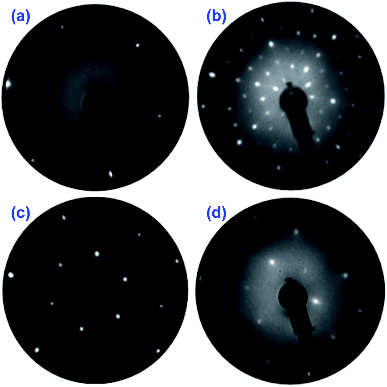 | ||
| Fig. 1 Low energy electron diffraction (LEED) patterns of (a) clean Pt(111) and (b–d) of Se film on Pt(111) annealed respectively at 400 °C, 600 °C and 750 °C. The LEED patterns were recorded at an energy of 80 eV. | ||
LT-STM was employed to examine the surface structure of the PtSe2 films at the atomic scale. After annealing at 400 °C, a well-defined moiré pattern of the PtSe2 was observed due to its mismatch with the Pt(111) surface (Fig. 2). The periodicity of the moiré pattern is approximately 11 Å, which is nearly 4 times the lattice constant of Pt(111). A hexagonal honeycomb arrangement is clearly visible in a zoomed area from the moiré pattern (Fig. 2b), for which a 2H trigonal prismatic coordination can be proposed. The atomic arrangement is also consistent with the TEM results on PtSe2 or other TMD systems in literature.42–46 The structure changed dramatically after annealing the sample at 600 °C as indicated in Fig. 2c and d, the previous 2H phase is replaced by a new (√3 × √3)R30° superstructure. This latter is a strong indication of formation of a surface alloy, type Pt2Se. One notices the presence of several bright domains on the surface that may originate from insufficient heating. Similar domains were observed by Zheng et al., and were interpreted as Se-rich antisite defects.47,48 After a further annealing at 750 °C, the unit cell of the Pt2Se undergoes a rotation of 30° compared with the (√3 × √3)R30° structure at 600 °C, resulting in a (2 × 2) pattern with respect to the Pt lattice, as seen in Fig. 2e and f. For the (2 × 2) structure, one observes a large density of defects on the surface which is consistent with the LEED pattern showing high-background and diffusing diffraction spots.
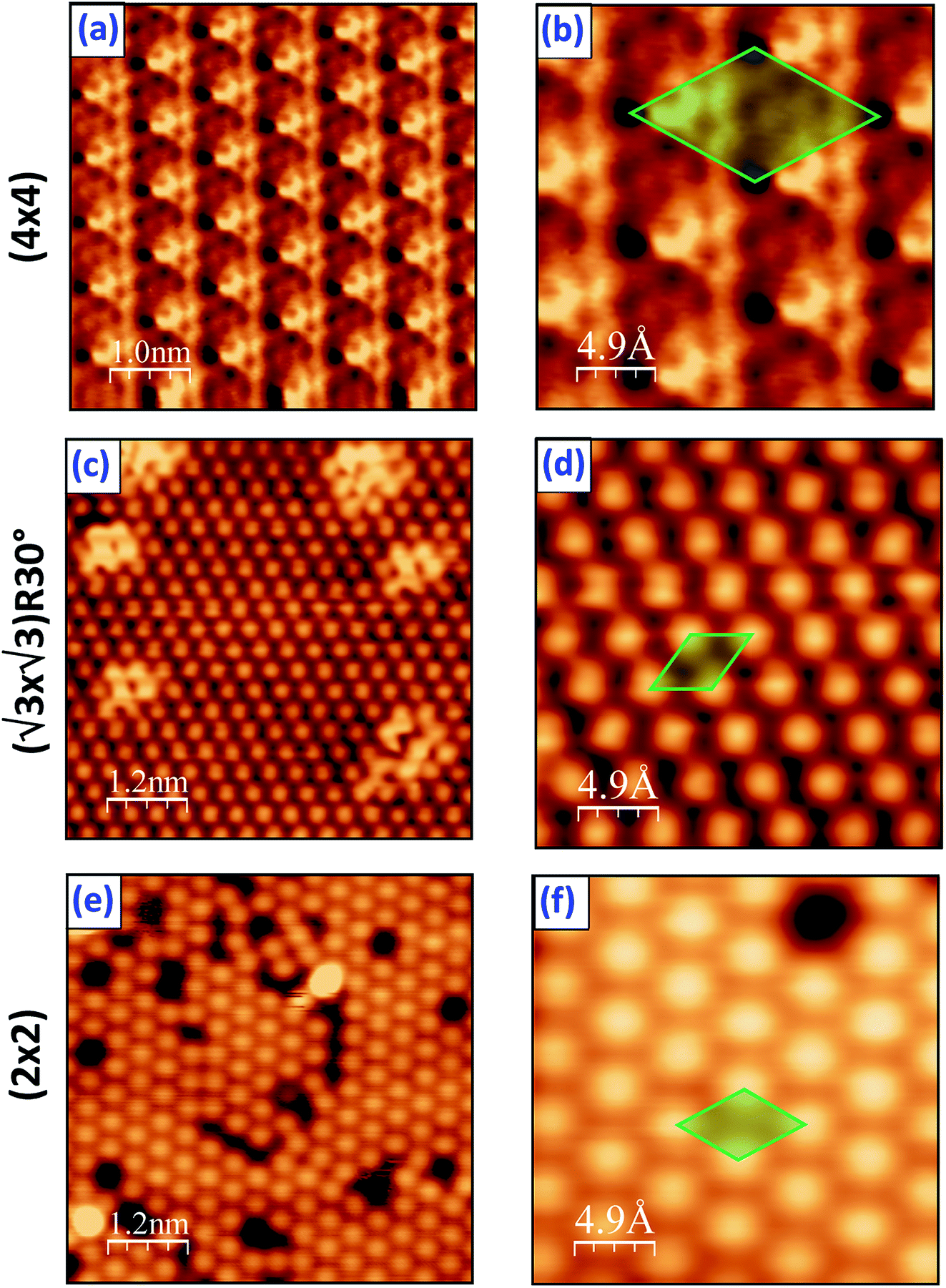 | ||
| Fig. 2 Atomic resolution STM images obtained on Pt(111) covered by Se film followed by annealing at: (a, b) 400 °C, (c, d) 600 °C and (e, f) 750 °C, respectively. | ||
III.2. Photoemission measurements
Fig. 3 shows an XPS overview spectrum measured on a freshly deposited Se film compared to those after annealing at 400 °C and at 600 °C, respectively. Several core level features are present like the Pt4f at 71 eV, the Se3d at 54 eV, and Se3p at 162 eV. One observes also a tiny C1s peak at 285 eV and almost no structure of the O1s at 531 eV. Such low contamination may come from uncontrolled exposure to air during the film preparation when the substrate was incubated in the Na2Se solution, although this operation was made under N2 flow condition. One notices also the absence of Na core level peaks. After annealing, the C intensity is considerably attenuated and that of O disappears almost completely. This proves a relative cleanliness of the surface and demonstrates that our method for the preparation of PtSe2 films can be generalized and widely used in different research and technological fields.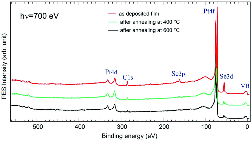 | ||
| Fig. 3 Overview spectra measured with hν = 700 on Pt(111) covered by as-grown Se film, after annealing at 400 °C, and after further annealing at 600 °C, respectively. Several features are observed like the Pt4f centred at 72 eV, Se3d at 54 eV, Se3p at 162 eV. Only a tiny C1s peak at 285 eV and almost no O1s structure at 531 eV are seen. These contaminations come from the air atmosphere during the film deposition where the substrate was incubated into the solution. Upon annealing the O and C are significantly attenuated. They shall not affect the PtSe2 formation so we don't talk about it in the following. | ||
Fig. 4 illustrates the evolution of photoemission spectra as a function of annealing temperature, together with the one measured on a clean Pt surface, at hν = 260 eV. At this energy, we mainly probe the Pt4f and Se3d core levels located around 71 eV and 54 eV, respectively. A significant difference in the peak intensity between these two levels is due to many parameters. In particular, one should take into consideration the respective cross section of excitation of the Se and Pt levels, as well as the electron mean free path. The measurement parameters like the transmission curve of the electron spectrometer also have an influence. Note that at 260 eV photon energy, the Se3p cross section is an order of magnitude smaller than that of Se3d and hence peaks due to the latter state are much more prominent.49 Also, the cross section of the Pt 5p (lying at about 51.5 eV) is about 30 times lower than of Pt4f and about 50 times lower than that of Se3d, thus it is not visible in the spectra presented here.49 This is why hereafter we refer solely to the CLBEs of the lower lying spin orbit components: Pt4f7/2 and Se3d5/2 and to the ratio between their peak intensities.
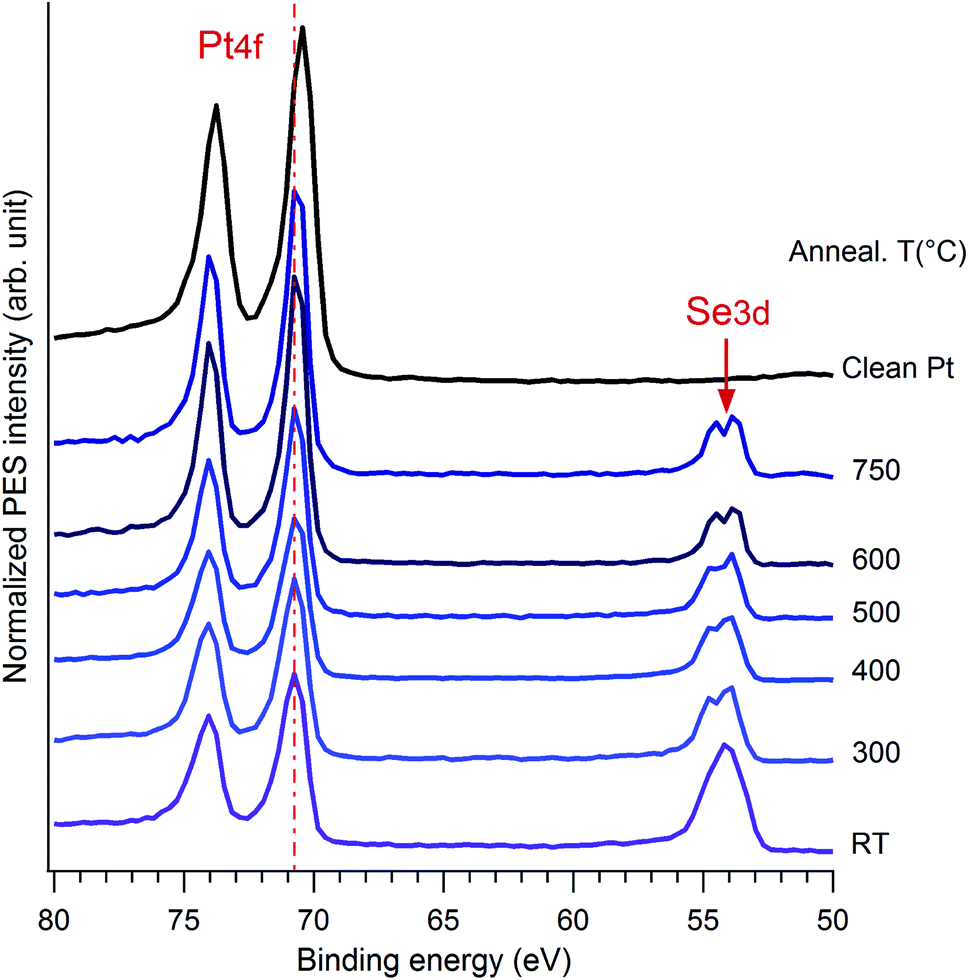 | ||
| Fig. 4 Set of XPS spectra measured on Pt(111) covered by Se layer and showing the evolution of the Pt4f and Se3d core level peaks as function of the annealing temperature, in comparison with spectrum obtained on pristine Pt(111). The data were recorded at 260 eV photon energy at normal emission. | ||
As a function of temperature, the first significant change, especially for the Se3d level, is observed when the film is heated to 300 °C. This is largely due to desorption of oxygen and carbon atoms, as well as bulk like Se atoms from the surface and the rearrangement of the surface structure. Then, an intensity balance occurs in the range of 300 °C to 600 °C and the spectral weight of Pt4f increases while that of Se3d decreases. This is a clear indication of desorption of the Se top-layers from the surface, allowing the reduction of the film thickness. No significant change is observed after annealing at temperature above 600 °C.
Now we take a closer look at the details of the XPS data. Upon annealing, we see a substantial change in the spectra of Pt4f and Se3d core levels, the details of which are given in Fig. 5. The angles indicated here correspond to the one between the emitted electron captured by the analyser and the surface plane. Thus 90° means the normal emission while the 20° is the grazing emission case. One can distinguish that the angular dependence only appears in the range of 300–400 °C of annealing, while it disappears at higher temperature, above 600 °C. A better understanding of the angular dependence behaviour required a fitting of the spectrum with two different components corresponding to the bulk contribution and the surface one, the latter of which in our case should be assigned to the Pt in the PtSe2 films as reported previously in literature. The surface component in the clean Pt spectrum was also proved by other authors.27,28
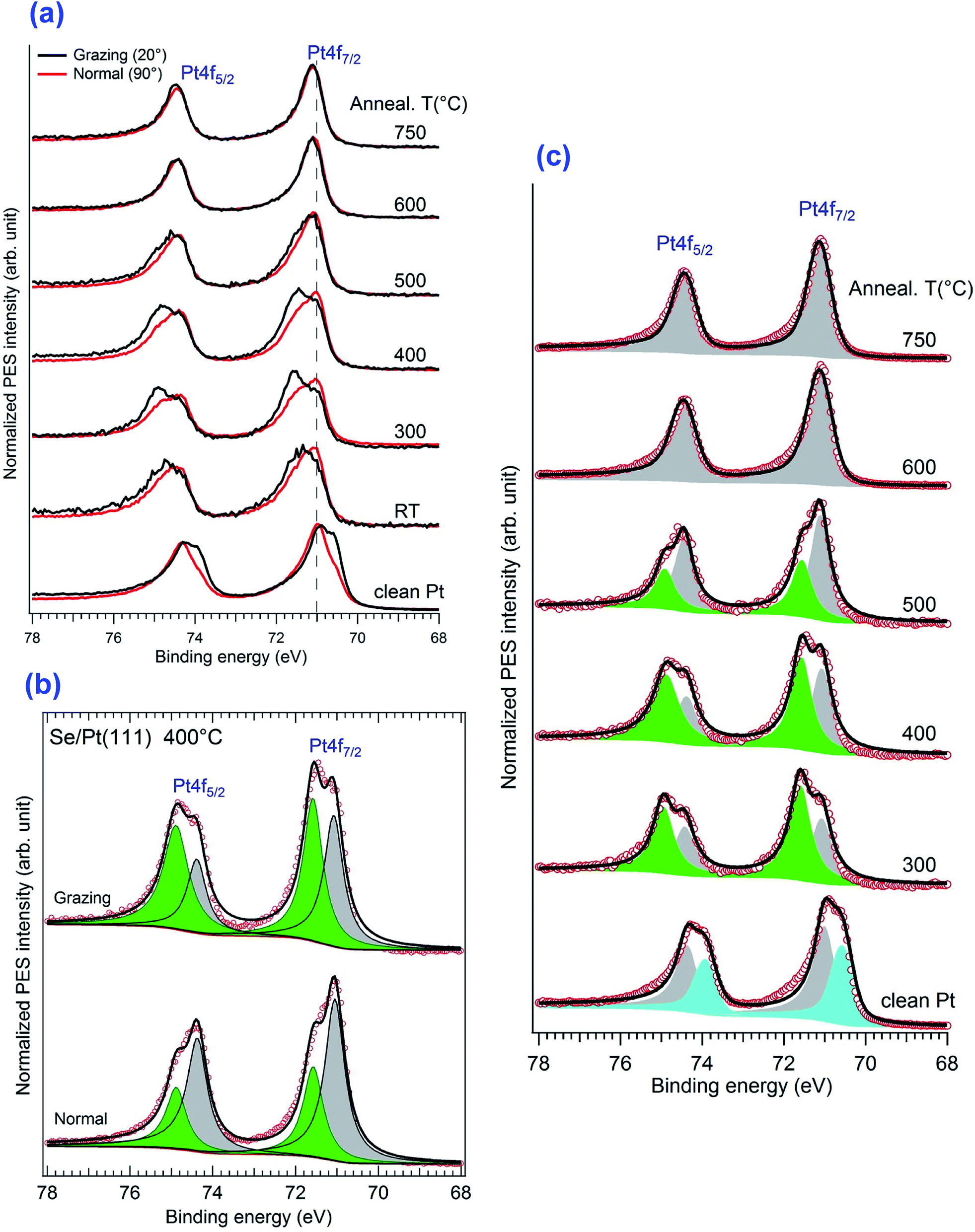 | ||
| Fig. 5 XPS spectra of the Pt4f features for normal and grazing emission on pristine and selenized Pt(111) surfaces. (a) Superposed normal and grazing emission spectra, (b) fitting of spectra obtained at 400 °C annealing temperature and (c) global view of the fitting of spectra obtained Grazing emission and at different annealing temperatures. | ||
As mentioned above, Doniach–Sunjic line-shapes were used to fit the Pt4f spectra, after subtraction of a Shirley background. Starting from the clean substrate, the Pt7/2 surface and bulk components are located at 70.5 eV and 71.1 eV, respectively. No oxidation features located at 72 eV or a hump at 76.9 eV was observed.50 The surface component is shifted to 71.4 eV upon initial selenization, which was similar to the PtO2 case.27,28 The two components co-exist from 300–500 °C and the PtSe2 component disappeared totally at 600 °C while the Pt bulk contribution increases slightly. In accordance to the overview results, the intensity ratio between the surface component and the bulk one kept decreasing upon annealing. The most prominent angular dependence at 400 °C was extracted in Fig. 5b. Measurements show that at grazing emission the higher energy component is considerably enhanced, indicating that it corresponds to Pt atoms in the vicinity of the surface. The general features of these spectra are similar to previous reports of oxidation of Pt27,28 and of the recent work on PtSe2 nano-layer formation.26 The low energy Pt7/2 contribution lying at 71.1 eV is associated with the Pt0 of the bulk covered by the sandwich-like SePtSe structure. The higher energy feature could be assigned to Pt2+, which was also given in PtNi system.51 Yim et al., gave the corresponding peak position at about 72.3 eV after annealing to 400 °C but for the case of a trilayer PtSe2 film26 the position of this peak evolves in case of oxidation. Thus, Miller et al., reported a CLBE of the highly oxidized Pt film of about 72.1 eV and a position of about 71.6 eV for lower oxygen exposure, although they consider a OPtO structure, which evolves from wire like formation to a monolayer film.28 They suggested that they may have up to two PtO2 layers in case of high oxidation. Possibly the CLBE for a single PtSe2 layer on Pt(111) is lower than in the multilayer case. We shall return to this point in the following. Upon annealing of the sample at 600 °C, the spectroscopic Pt2+ feature at 71.4 eV vanishes completely. This result is a strong evidence of the disappearance of the 2H phase, i.e. of SePtSe sandwich structure and occurs to be in great agreement the LEED and STM outcome suggesting the formation of a single monolayer of Pt2Se surface alloy. Interestingly, when the remaining surface was heated at temperature higher than 750 °C, the surface component of the clean Pt, which previously shifts to a higher binding energy of 71.1 eV in the Se containing structure, started to appear again at binding energy 70.6 eV, which is assigned to the surface component of clean Pt(111). This means that the Pt2Se has vanished through desorption process of the Se atoms induced at high temperature.
The evolution of the Se3d core level versus annealing temperature is illustrated in Fig. 6. After initial selenization, the spectrum shows multi-component Se3d5/2 peaks with a shoulder at 54.0 eV and a main peak at 54.6 eV. In previous studies of Se adsorption from Na2Se on Au and Cu it was noted that initial adsorption leads to appearance of selenium corresponding to metal selenide, chemisorbed Se atoms, and also to some ring or bulk like components.31,33 Because of the very low melting point of bulk Se (tabulated value of 221 °C) one can suppose that any bulk like Se would be rapidly eliminated upon heating, leaving more strongly bound components. The structures are quite similar when annealing at 300 °C to 500 °C, more or less resolving two components. But an angular dependence is observed only for the 400 °C and 500 °C cases, although is less visible for 500 °C. The detailed fitting of the Se3d spectrum is given in Fig. 6 with the Voigt fitting procedure after the Shirley background subtraction. The fitting parameters were constrained to reduce the uncertainty: the Se3d spin orbital split of 0.86 eV and a ratio of 2/3 were utilized. All the Voigt width was kept at 0.55 eV. As indicated here, from 300 °C to 500 °C the spectra were de-convoluted with two main doublets with the 3d5/2 CLBE locating at 54.2 eV and 54.6 eV, respectively. In earlier work, Yim et al., reported a somewhat broad and structure-less Se 3d5/2 spectrum with a CLBE given to be 54.6 eV for a trilayer film. Wang et al. report a structured spectrum with a maximum (Se3d5/2) at about 54.7 eV and a shoulder at 54.3 eV at 200 °C. At 270 °C they present a broad doublet with a 3d5/2 CLBE of 54.3 eV for the monolayer film. In our case it was close to the monolayer structure. The angular dependence at 400 °C, in which the 54.3 eV component became more predominant at grazing angle, also clearly indicated a SePtSe trilayer structure with the 54.2 eV peak assigned to the upper Se atoms of the trilayer. The spectroscopic feature positioned at 54.6 eV is associated with the down Se atoms located between the bulk Pt atoms and the Pt atoms of the SePtSe trilayer.
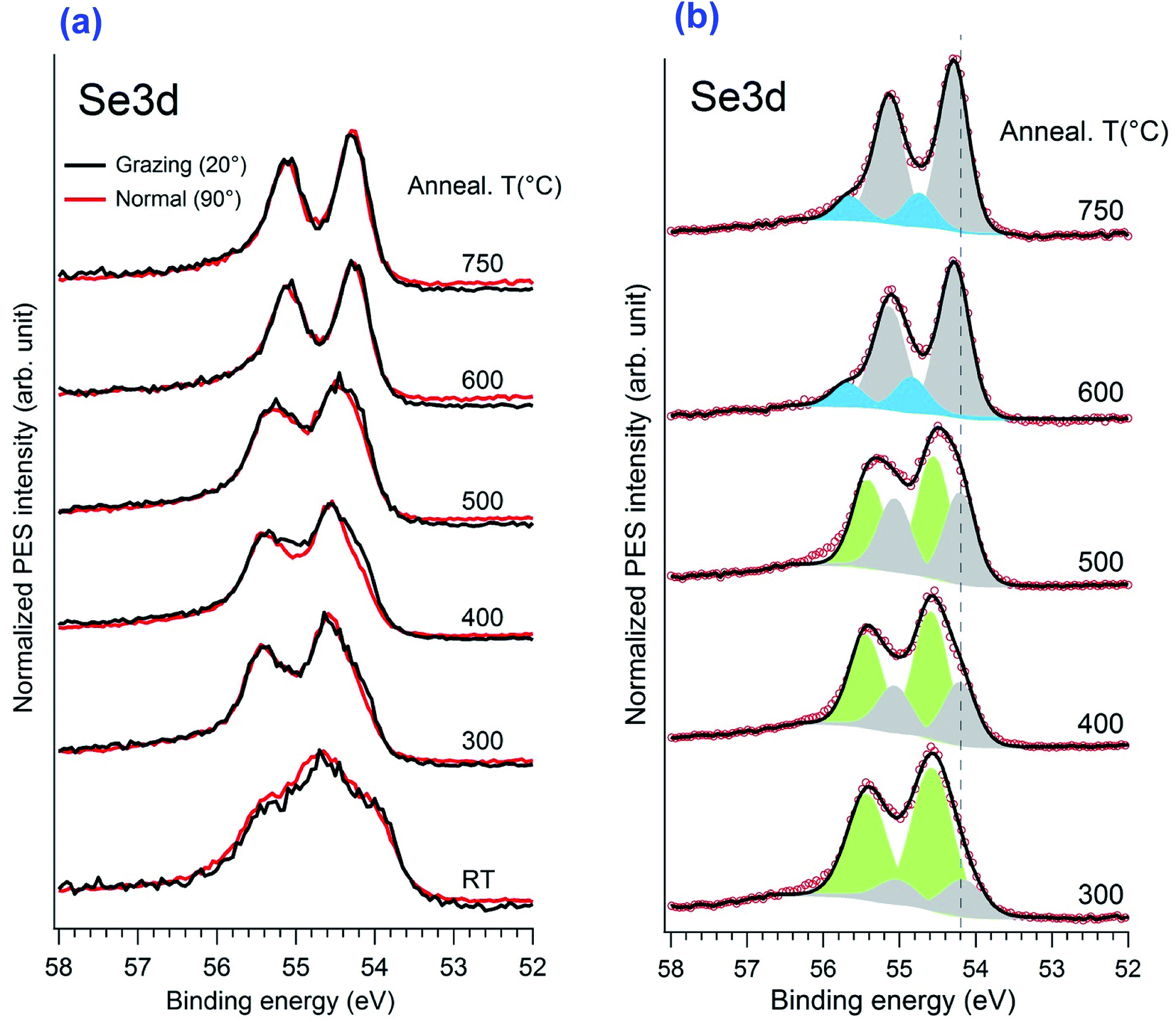 | ||
| Fig. 6 (a) XPS spectra illustrating the evolution of the Se 3d core level peaks as a function of annealing temperature for normal and grazing emission geometries. (b) Fitting of Se3d spectra at different annealing temperatures measured at normal emission. | ||
Significant change of the peak shape happened only after annealing at temperature higher than 600 °C. The upper Se component shifts only slightly to 54.3 eV while the higher energy component vanishes totally and no angular dependence is observed. Moreover, the ratio in the XPS spectral weight between the Se3d and Pt4f peaks decreases significantly, which is consistent with the fact that only one Se–Pt monolayer exists on the surface. One notices the occurrence of a new feature with low spectral weight at a binding energy of 54.9 eV (blue peak in Fig. 6), which is most likely attributed to the defect regions rich in Se atoms.
IV. Discussion
We do not discuss the properties of the film below 300 °C because no LEED patterns or STM images could be observed, indicating either the non-homogeneous structure of the surface below this temperature or the presence of a considerable amount of Se deposit. The second reason is more likely, as it could explain the similarity of Se3d and Pt4f spectra to those obtained after annealing at 400 °C. We would mainly focus on the 400–600 °C phases, as they offer us interesting structural information. The surface displayed a good SePtSe trilayer after the reconstruction at 400 °C. The LEED showed a (4 × 4) structure of the PtSe2 layer with respect to the Pt(111) surface lattice. LT-STM provided a moiré pattern of the PtSe2, which corresponds to the model of trigonal prismatic coordination proposed elsewhere.19 This was commonly seen in the MoS2 and other metal chalchogenide structure.42,52Phase transition in TMD systems represents an interesting aspect to investigate. Transition from the 2H phase to a metallic 3R phase was reported on exfoliated MoS2 nanosheets.53 Besides, a 1T to 2H phase transition was observed in MoS2 due to the intercalation with alkali metal or by doping.54–58 The phenomenon was explained by the transfer of electron from the s orbital of the alkali metal to the d orbital of the transition metal, which attributes to the destabilization of the 1T phase. In other cases, a different evolution from 2H-TMD to a surface alloy monolayer, with a clear boundary between the two phases due to the partial phase transition, has been observed.42,59 The transitions of 1T or the 2H structure of the PtSe2 have been reported using different synthesis methods,21,26,30 but to our knowledge, no phase transition to a surface alloy monolayer has been reported. In our present study, we highlighted through systematic analysis a transition from 2H-PtSe2 phase to a Pt2Se alloy monolayer. The PtSe2 firstly displayed a 2H trigonal prismatic phase, in which the Pt atom was prismatically bonded to six Se atoms after annealing at 400–500 °C. Interestingly, the (4 × 4) structure is nicely observed by the HR-STM, where a moiré pattern with honeycomb arrangement is seen, in perfect agreement with the LEED investigations. The similarity of the Se3d core level in the 300–500 °C range indicated the same architectural properties in the PtSe2 films. Further annealing, inducing desorption of Se atoms, leads to formation of a Pt2Se alloy monolayer characterized by its (√3 × √3)R30° superstructure. This alloy phase is known to develop commonly in a large number of systems, like Cu2Te/Cu(111),9 Ag2Bi/Ag(111),60,61 Cu2Bi/Cu(111),62 Ag2Sb/Ag(111),63 and others. Such a phase transition induced the significant altering of the chemical bonding state of the Pt and Se. This is reflected in the Pt4f and Se3d core level spectra, in both of which the previously multi-components spectrum turned into a single dominant component spectrum, leaving just mainly the bulk Pt and Se2+ features, respectively. At higher temperature, another surface structure occurs and exhibits a (2 × 2) superstructure observed by LEED and confirmed by LT-STM. This latter is characterized by a relatively high density of defects.
V. Conclusion
In summary, we have highlighted a new approach for the preparation of two-dimensional TMD monolayer, in particular for the PtSe2 system. It consists in chemical deposition upon immersion of Pt(111) surface into the Na2Se aqueous solution. Although this method is rather simple, it provides high quality and well-ordered films on a large scale. A carbon- and oxygen-free surface is obtained after a moderate annealing procedure. Depending on the annealing temperature of the sample, the surface undergoes different phase transitions. LEED investigations revealed a transition from (4 × 4) to (√3 × √3)R30° and then to a (2 × 2) superstructures, which is also confirmed by STM showing structural transformation from 2H-PtSe2 to Pt2Se alloy monolayer. Analysis of the XPS data proves the presence of different chemical environments and the structural transitions influence directly the electronic structure. This work provides an alternative method for the fabrication of large-scale 2D transition metal dichalchogenide films, as well as single alloy layer.Conflicts of interest
The authors declare no conflicts of interest.Acknowledgements
Y. T. is grateful to the China Scholarship Council for supporting his PhD work in France. A. B. acknowledges the Synchrotron SOLEIL direction for supporting this project. We thank also the TEMPO beamline staff for the technical support.References
- A. K. Geim, Graphene: Status and Prospects, Science, 2009, 324, 1530–1534 CrossRef CAS.
- X. Yu, H. Cheng, M. Zhang, Y. Zhao, L. Qu and G. Shi, Graphene-Based Smart Materials, Nat. Rev. Mater., 2017, 2, 17046 CrossRef CAS.
- L. Tao, E. Cinquanta, D. Chiappe, C. Grazianetti, M. Fanciulli, M. Dubey, A. Molle and D. Akinwande, Silicene Field-Effect Transistors Operating at Room Temperature, Nat. Nanotechnol., 2015, 10, 227–231 CrossRef CAS PubMed.
- H. Oughaddou, H. Enriquez, M. R. Tchalala, H. Yildirim, A. J. Mayne, A. Bendounan, G. Dujardin, M. Ait-Ali and A. Kara, Silicene, a Promising New 2D Material, Prog. Surf. Sci., 2015, 90, 46–83 CrossRef CAS.
- S. Sadeddine, H. Enriquez, A. Bendounan, P. K. Das, I. Vobornik, A. Kara, A. J. Mayne, F. Sirotti, G. Dujardin and H. Oughaddou, Sci. Rep., 2017, 7, 44400 CrossRef.
- L. Li, S.-Z. Lu, J. Pan, Zh. Qin, Y.-Q. Wang, Y. Wang, G.-Y. Cao, Sh. Du and H.-J. Gao, Buckled Germanene Formation on Pt(111), Adv. Mater., 2014, 26, 4820–4824 CrossRef CAS PubMed.
- W. Zhang, H. Enriquez, Y. Tong, A. Bendounan, A. Kara, A. P. Seitsonen, A. J. Mayne, G. Dujardin and H. Oughaddou, Epitaxial Synthesis of Blue Phosphorene, Small, 2018, 14, 1804066 CrossRef PubMed.
- L. Li, Y. Wang, Sh. Xie, X.-B. Li, Y.-Q. Wang, Sh. Zhang and H.-J. Gao, Two-Dimensional Transition Metal Honeycomb Realized: Hf on Ir(111), Nano Lett., 2013, 13, 4671–4674 CrossRef CAS.
- Y. Tong, M. Bouaziz, W. Zhang, B. Obeid, A. Loncle, H. Oughaddou, H. Enriquez, K. Chaouchi, V. Esaulov, Z. Chen, H. Xiong, Y. Cheng and A. Bendounan, Evidence of New 2D Material: Cu2Te, 2D Mater., 2020, 7, 035010 CrossRef.
- Z. Zhang, Z. Chen, M. Bouaziz, Ch. Giorgetti, H. Yi, J. Avila, B. Tian, A. Shukla, L. Perfetti, D. Fan, Y. Li and A. Bendounan, Direct Observation of Band Gap Renormalization in Layered Indium Selenide, ACS Nano, 2019, 13, 13486–13491 CrossRef CAS.
- H. Wang, H. Yuan, S. S. Hong, Y. Li and Y. Cui, Physical and Chemical Tuning of Two-Dimensional Transition Metal Dichalcogenides, Chem. Soc. Rev., 2015, 44, 2664–2680 RSC.
- J. Jia, A. Kara, L. Pasquali, A. Bendounan, F. Sirotti and V. A. Esaulov, On Sulfur Core Level Binding Energies in Thiol Self-Assembly and Alternative Adsorption Sites: An Experimental and Theoretical Study, J. Chem. Phys., 2015, 143, 104702 CrossRef PubMed.
- Y. Tong, T. Jiang, A. Bendounan, M. N. K. Harish, A. Giglia, S. Kubsky, F. Sirotti, L. Pasquali, S. Sampath and V. A. Esaulov, Case Studies on the Formation of Chalcogenide Self-Assembled Monolayers on Surfaces and Dissociative Processes, Beilstein J. Nanotechnol., 2016, 7, 263–277 CrossRef CAS.
- A. Splendiani, L. Sun, Y. Zhang, T. Li, J. Kim, C.-Y. Chim, G. Galli and F. Wang, Emerging Photoluminescence in Monolayer MoS2, Nano Lett., 2010, 10, 1271–1275 CrossRef CAS.
- Y. Zhao, J. Qiao, P. Yu, Z. Hu, Z. Lin, S. P. Lau, Z. Liu, W. Ji and Y. Chai, Extraordinarily Strong Interlayer in 2D Layered PtS2, Adv. Mater., 2016, 28, 2399–2407 CrossRef CAS PubMed.
- A. Abouimrane, D. Dambournet, K. W. Chapman, P. J. Chupas, W. Weng and K. Amine, A New Class of Lithium and Sodium Rechargeable Batteries Based on Selenium and Selenium-Sulfur as a Positive Electrode, J. Am. Chem. Soc., 2012, 134(10), 4505–4508 CrossRef CAS.
- H. W. Schock, Thin Film Photovoltaics, Appl. Surf. Sci., 1996, 92, 606–616 CrossRef CAS.
- S. Zein El Abedin, A. Y. Saad, H. K. Farag, N. Borisenko, Q. X. Liu and L. F. Endres, Electrodeposition of Selenium, Indium and Copper in an Air and Water-Stable Ionic Liquid at Variable Temperatures, Electrochim. Acta, 2007, 52, 2746–2754 CrossRef CAS.
- Y. Wang, et al., Monolayer PtSe2, a New Semiconducting Transition-Metal-Dichalcogenide, Epitaxially Grown by Direct Selenization of Pt, Nano Lett., 2015, 15, 4013–4018 CrossRef CAS PubMed.
- M. Buscema, D. J. Groenendijk, G. A. Steele, H. S. J. van der Zant and A. Castellanos-Gomez, Photovoltaic Effect in Few-Layer Black Phosphorus PN Junctions Defined by Local Electrostatic Gating, Nat. Commun., 2014, 5, 4651 CrossRef CAS.
- M. O'Brien, et al., Raman Characterization of Platinum Diselenide Thin Films, 2D Materials, 2016, 3(2), 021004 CrossRef.
- E. S. Reich, Phosphorene Excites Materials Scientists, Nature, 2014, 506, 19 CrossRef PubMed.
- J. Dai and X. C. Zeng, Bilayer Phosphorene: Effect of Stacking Order on Bandgap and Its Potential Application in Thin-Film Solar Cells, J. Phys. Chem. Lett., 2014, 5(7), 1289–1293 CrossRef CAS.
- P. Li, L. Li and X. C. Zeng, Tuning the Electronic Properties of Monolayer and Bilayer PtSe2 via Strain Engineering, J. Mater. Chem. C, 2016, 4, 3106–3112 RSC.
- K. Ullah, L. Zhu, Z.-D. Meng, S. Ye, S. Sarkar and W.-Ch. Oh, Synthesis and characterization of novel PtSe2/graphene nanocomposites and its visible light driven catalytic properties, J. Mater. Sci., 2014, 49, 4139–4147 CrossRef CAS.
- Ch. Yim, K. Lee, N. McEvoy, M. O'Brien, S. Riazimehr, N. C. Berner, C. P. Cullen, J. Kotakoski, J. C. Meyer, M. C. Lemme and G. S. Duesberg, High-Performance Hybrid Electronic Devices from layered PtSe2 Films Grown at Low Temperature, ACS Nano, 2016, 10, 9550–9558 CrossRef CAS.
- C. Puglia, A. Nilsson, B. Hernnäs, O. Karis, P. Bennich and N. Martensson, Physisorbed, chemisorbed and dissociated O2 on Pt(111) studied by different core level spectroscopy methods, Surf. Sci., 1995, 342, 119–133 CrossRef CAS.
- D. J. Miller, H. Öberg, S. Kaya, H. Sanchez Casalongue, D. Friebel, T. Anniyev, H. Ogasawara, H. Bluhm, L. G. M. Pettersson and A. Nilsson, Oxidation of Pt(111) under Near-Ambient Conditions, Phys. Rev. Lett., 2011, 107, 195502 CrossRef CAS PubMed.
- C. Ellinger, A. Stierle, I. K. Robinson, A. Nefedov and H. Dosch, Atmospheric pressure oxidation of Pt(111), J. Phys.: Condens. Matter, 2008, 20, 184013 CrossRef.
- Z. Wang, Q. Li, F. Besenbacher and M. Dong, Facile Synthesis of Single Crystal PtSe2 Nanosheets for Nanoscale Electronics, Adv. Mater., 2016, 28, 10224–10229 CrossRef CAS.
- J. Jia, A. Bendounan, H. M. N. Kotresh, K. Chaouchi, F. Sirotti, S. Sampath and V. A. Esaulov, Selenium Adsorption on Au(111) and Ag(111) Surfaces: Adsorbed Selenium and Selenide Films, J. Phys. Chem. C, 2013, 117, 9835–9842 CrossRef CAS.
- J. Jia, A. Bendounan, K. Chaouchi, S. Kubsky, F. Sirotti, L. Pasquali and V. A. Esaulov, Chalcogen Atom Interaction with Palladium and the Complex Molecule-Metal Interface in Thiol Self Assembly, J. Phys. Chem. C, 2014, 118, 24983–24994 CrossRef CAS.
- Y. Tong, T. Jiang, A. Bendounan, F. Nicolas, S. Kubsky and V. A. Esaulov, Selenium, Benzeneselenol, and Selenophene Interaction with Cu(100), J. Phys. Chem. C, 2016, 120(38), 21486–21495 CrossRef CAS.
- M. Fathinezhad, M. A. Tarighat and D. Dastan, Chemometrics Heavy Metal Content Clusters Using Electrochemical Data of Modified Carbon Paste Electrode, Environ. Nanotechnol. Monit. Manag., 2020, 14, 1003 Search PubMed.
- D. Dastan, Effect of Preparation Methods on the Properties of Titania Nanoparticles: Solvothermal versus Sol-Gel, Appl. Phys. A, 2017, 123, 699 CrossRef.
- D. Dastan, N. Chaure and M. Kartha, Surfactants Assisted Solvothermal Derived Titania nanoparticles: Synthesis and Simulation, J. Mater. Sci.: Mater. Electron., 2017, 28, 7784–7796 CrossRef CAS.
- D. Dastan, S. Panahi and N. Chaure, Characterization of Titania Thin Films Grown by Dip-Coating Technique, J. Mater. Sci.: Mater. Electron., 2016, 27, 12291–12296 CrossRef CAS.
- D. Dastan, P. U. Londhe and N. B. Chaure, Characterization of TiO2 Nanoparticles Prepared Using Different Surfactants by Sol–Gel Method, J. Mater. Sci.: Mater. Electron., 2014, 25, 3473–3479 CrossRef CAS.
- J. R. Arthur, Molecular Beam Epitaxy, Surf. Sci., 2002, 500, 189–217 CrossRef CAS.
- Molecular Beam Epitaxy, Fundamental and Current Status, Springer Series in Materials Science, ed. M. A. Herman and H. Sitter, Springer, Berlin, Heidelberg, 2012 Search PubMed.
- N. Fairley, CasaXPS: Processing Software for XPS, AES, SIMS and More, Casa Software Ltd., 2018 Search PubMed.
- L. Zhou, K. Xu, A. Zubair, A. D. Liao, W. Fang, F. Ouyang, Y.-H. Lee, K. Ueno, R. Saito, T. Palacios, J. Kong and M. S. Dresselhaus, Large-Area Synthesis of High-Quality Uniform Few-Layer MoTe2, J. Am. Chem. Soc., 2015, 137(37), 11892–11895 CrossRef CAS.
- M. Chhowalla, H. S. Shin, G. Eda, L.-J. Li, K. P. Loh and H. Zhang, The Chemistry of Two-Dimensional Layered Transition Metal Dichalcogenide Nanosheets, Nat. Chem., 2013, 5, 263–275 CrossRef.
- G. Eda, T. Fujita, H. Yamaguchi, D. Voiry, M. Chen and M. Chhowalla, Coherent Atomic and Electronic Heterostructures of Single-Layer MoS2, ACS Nano, 2012, 6, 7311–7317 CrossRef CAS PubMed.
- W. Zhou, X. Zou, S. Najmaei, Zh. Liu, Y. Shi, J. Kong, J. Lou, P. M. Ajayan, B. I. Yakobson and J.-C. Idrobo, Intrinsic Structural Defects in Monolayer Molybdenum Disulfide, Nano Lett., 2013, 13, 2615–2622 CrossRef CAS.
- J. Brivio, D. T. L. Alexander and A. Kis, Ripples and Layers in Ultrathin MoS2 Membranes, Nano Lett., 2011, 11, 5148–5153 CrossRef CAS.
- H. Zheng, H. Choi, F. Baniasadi, D. Hu, L. Jiao, K. Park and Ch. Tao, Visualization of Point Defects in Ultrathin Layered 1T-PtSe2, 2D Mat, 2019, 6(4), 041005 CrossRef CAS.
- J. Gao, Y. Cheng, T. Tian, X. Hu, K. Zeng, G. Zhang and Y.-W. Zhang, Structure, Stability, and Kinetics of Vacancy Defects in Monolayer PtSe2: A First-Principles Study, ACS Omega, 2017, 2, 8640–8648 CrossRef CAS PubMed.
- J. J. Yeh and I. Lindau, Atomic Subshell Photoionization Cross Sections and Asymmetry Parameters: 1 ≤ Z ≤ 103, At. Data Nucl. Data Tables, 1985, 32, 1–155 CrossRef CAS.
- J. F. Weaver, J.-J. Chen and A. L. Gerrard, Oxidation of Pt(111) by Gas-Phase Oxygen Atoms, Surf. Sci., 2005, 592, 83–103 CrossRef CAS.
- X. Liu, G. Xu, Y. Chen, T. Lu, Y. Tang and W. Xing, A Strategy for Fabricating Porous PdNi@Pt Core-shell Nanostructures and Their Enhanced Activity and Durability for the Methanol Electrooxidation, Sci. Rep., 2015, 5, 7619 CrossRef CAS.
- W. Zhou, X. Zou, S. Najmaei, Zh. Liu, Y. Shi, J. Kong, J. Lou, P. M. Ajayan, B. I. Yakobson and J.-C. Idrobo, Intrinsic Structural Defects in Monolayer Molybdenum Disulfide, Nano Lett., 2013, 13, 2615–2622 CrossRef CAS.
- A. N. Enyashin, L. Yadgarov, L. Houben, I. Popov, M. Weidenbach, R. Tenne, M. Bar-Sadan and G. Seifert, New Route for Stabilization of 1T-WS2 and MoS2 Phases, J. Phys. Chem. C, 2011, 115, 24586–24591 CrossRef CAS.
- J. A. Wilson and A. D. Yoffe, The Transition Metal Dichalcogenides Discussion and Interpretation of the Observed Optical, Electrical and Structural properties, Adv. Phys., 1969, 18, 193–335 CrossRef CAS.
- R. Bissessur, M. G. Kanatzidis, J. L. Schindler and C. R. Kannewurf, Encapsulation of Polymers Into MoS2 and Metal to Insulator Transition in Metastable MoS2, J. Chem. Soc., Chem. Commun., 1993, 20, 1582–1585 RSC.
- R. F. Frindt and A. D. Yoffe, Physical Properties of Layer Structures: Optical Properties and Photoconductivity of Thin Crystals of Molybdenum Disulphide, Proc. R. Soc. London, Ser. A, 1963, 273, 69–83 Search PubMed.
- M. A. Py and R. R. Haering, Structural Destabilization Induced by Lithium Intercalation in MoS2 and Related-Compounds, Can. J. Phys., 1983, 61, 76–84 CrossRef CAS.
- P. Ganal, W. Olberding, T. Butz and G. Ouvrard, Soft Chemistry Induced Host Metal Coordination Change from Octahedral to Trigonal Prismatic 1T-TaS2, Solid State Ionics, 1993, 59, 313–319 CrossRef CAS.
- G. Eda, H. Yamaguchi, D. Voiry, T. Fujita, M. Chen and M. Chhowalla, Photoluminescence from Chemically Exfoliated MoS2, Nano Lett., 2011, 11, 5111–5116 CrossRef CAS PubMed.
- C. R. Ast, J. Henk, A. Ernst, L. Moreschini, M. C. Falub, D. Pacilé, P. Bruno, K. Kern and M. Grioni, Giant Spin Splitting through Surface Alloying, Phys. Rev. Lett., 2007, 98, 186807 CrossRef.
- L. Moreschini, A. Bendounan, C. R. Ast, F. Reinert, M. Falub and M. Grioni, Effect of Rare-Gas Adsorption on the Spin-Orbit Split Bands of a Surface Alloy: Xe on Ag(111)-(√3x√3)R30°-Bi, Phys. Rev. B, 2008, 77, 115407 CrossRef.
- L. Moreschini, A. Bendounan, H. Bentmann, M. Assig, K. Kern, F. Reinert, J. Henk, C. R. Ast and M. Grioni, Influence of the Substrate on the Spin-Orbit Splitting in Surface Alloys on (111) Noble Metal Surfaces, Phys. Rev. B, 2009, 80, 035438 CrossRef.
- L. Moreschini, A. Bendounan, I. Gierz, C. R. Ast, H. Mirhosseini, H. Höchst, K. Kern, J. Henk, A. Ernst, S. Ostanin, F. Reinert and M. Grioni, Assessing the Atomic Contribution to the Rashba Spin-Orbit Splitting in Surface Alloys: Sb/Ag(111), Phys. Rev. B, 2009, 79, 075424 CrossRef.
| This journal is © The Royal Society of Chemistry 2020 |