
 Open Access Article
 This Open Access Article is licensed under a Creative Commons Attribution-Non Commercial 3.0 Unported Licence
Photoelectrical properties of graphene/doped GeSn vertical heterostructures†
Yanhui Lva,
Hui Lib,
Cormac Ó Coileáinf,
Duan Zhangc,
Chenglin Henga,
Ching-Ray Changd,
K.-M. Hunge,
Huang Hsiang Cheng*b and
Han-Chun Wu *a
*a
aSchool of Physics, Beijing Institute of Technology, Beijing 100081, P. R. China. E-mail: wuhc@bit.edu.cn
bCenter for Condensed Matter Sciences, Graduate Institute of Electronics Engineering, National Taiwan University, Taipei 106, Taiwan, ROC. E-mail: hhcheng@ntu.edu.tw
cElementary Educational College, Beijing Key Laboratory for Nano-Photonics and Nano-Structure, Capital Normal University, Beijing 100048, P. R. China
dDepartment of Physics, National Taiwan University, Taiwan, ROC
eDepartment of Electronics Engineering, National Kaohsiung University of Science and Technology, Kaohsiung 807, Taiwan, ROC
fCRANN and AMBER, School of Chemistry, Trinity College Dublin, Dublin 2, Ireland
First published on 2nd June 2020
Abstract
GeSn is a group IV alloy material with a narrow bandgap, making it favorable for applications in sensing and imaging. However, strong surface carrier recombination is a limiting factor. To overcome this, we investigate the broadband photoelectrical properties of graphene integrated with doped GeSn, from the visible to the near infrared. It is found that photo-generated carriers can be separated and transported with a higher efficiency by the introduction of the graphene layer. Considering two contrasting arrangements of graphene on p-type and n-type GeSn films, photocurrents were suppressed in graphene/p-type GeSn heterostructures but enhanced in graphene/n-type GeSn heterostructures when compared with control samples without graphene. Moreover, the enhancement (suppression) factor increases with excitation wavelength but decreases with laser power. An enhancement factor of 4 is achieved for an excitation wavelength of 1064 nm. Compared with previous studies, it is found that our graphene/n-type GeSn based photodetectors provide a much wider photodetection range, from 532 nm to 1832 nm, and maintain comparable responsivity. Our experimental findings highlight the importance of the induced bending profile on the charge separation and provides a way to design high performance broadband photodetectors.
Introduction
GeSn is a group IV alloy material with a narrow bandgap,1,2 making it favorable for a variety of areas such as sensing and imaging. Recently, its photodetection and electroluminescence capabilities were demonstrated.3–5 However, GeSn suffers from strong carrier recombination at the surface, which significantly reduces the responsivity of GeSn based photodetectors.6 Graphene, a single-atom-thick carbon sheet, exhibits many excellent properties that are of interest for both fundamental science and technological progress.7,8 The contact of the basal plane of a graphene layer with a semiconductor creates a light-sensitive “surface junction” with a bending profile that transports electrons and holes across the junction.9 Numerous graphene/semiconductor heterojunctions have been proposed and fabricated,10–16 and several unique functionalities have been demonstrated.10,16–18 Recently, several studies also tried to integrate graphene with intrinsic GeSn to solve the issue of surface carrier recombination.4,19 They found photocurrent was improved in shortwave infrared range but suppressed in visible or near infrared range.19 It is known that the photoelectrical properties of graphene/semiconductor heterojunctions depend crucially on the bending profile, which can be tuned by doping the semiconductor.10 Moreover, most photodetectors use visible or near infrared light to read and record information. Thus, it is important to investigate the photoelectrical properties of graphene/doped GeSn heterojunctions and achieve an enhancement of the photocurrent over a broadband range.Here, we investigated the photoelectrical properties of graphene integrated with both n-type and p-type GeSn from the visible to the near infrared range. A responsivity of 200 mA W−1 and a broadband photodetection range from 532 nm to 1832 nm is achieved for photodetectors based on graphene/n-type GeSn heterostructures. Moreover, it is found that the photocurrents are enhanced in graphene/n-type GeSn heterostructures but suppressed in graphene/p-type GeSn heterostructures compared to samples without graphene layers. The enhancement (suppression) factor increases with excitation wavelength but decreases with laser power. Our results suggest that the integration of graphene with GeSn can separate and transport photo-generated carriers in higher efficiency.
Materials and methods
In this study, GeSn films with a thickness of 160 nm were grown by molecular beam epitaxy on n-type Ge wafers with a Sn content of 3.2% using a solid source molecular beam epitaxy (MBE) system with a base pressure of 8 × 10⁻¹⁰ Torr.6,20 Ge and Sn were co-deposited and the atomic ratio was controlled using an electronic gun (e-gun) and a double filament effusion cell respectively. To form n- and p-type GeSn, GeSn films were doped with P and B with concentrations in the order of 1015 cm−3. Fig. S1† shows a (004) ω–2θ scan of a 160 nm thick GeSn film on a Ge substrate. One can see that the incorporation of Sn modified the energy band of the host Ge and a bandgap of 0.63 eV was determined based on the parameters set out in ref. 6. Graphene was synthesized on a plasma treated Cu pocket via chemical vapor deposition.21–23 Prior to growth, the Cu pocket was annealed at 1035 °C for 40 min with a hydrogen flow rate of 10 sccm to remove surface oxidization and contamination. The synthesis of graphene was carried out at 1035 °C for 40 min under a methane and a hydrogen flow. After CVD growth, the graphene was transferred onto GeSn films with the assistance of polymethylmethacrylate (PMMA). Fig. S2† shows the Raman spectra of a typical graphene/GeSn heterostructure, where the Raman analysis was carried out using a Bruker Raman microscope with an excitation wavelength of 532 nm. There are three characteristic peaks located at 300, 1591, and 2684 cm−1, which correspond to the Ge–Ge mode of GeSn,24,25 and G band and 2D band of graphene26 respectively. The 2D band is sharp and symmetric, indicating high quality. Moreover, its intensity is more than twice of the G band indicating the transferred graphene is monolayer in nature.27 Metal electrodes were deposited onto the samples using an E-beam evaporator with the aid of a hard mask. The thickness of the metal electrodes was 100 nm.Results and discussion
Fig. 1a and b show schematics of the p-type doped-GeSn and graphene/p-type doped-GeSn heterostructure devices. The measurements were performed using a conventional two-probe-method and the separation between the adjacent electrical contacts was 0.5 mm. Au electrodes were deposited using an E-beam evaporator with a hard mask. The laser was focused centered between adjacent probes with a spot size of 0.25 mm. The photocurrent IPC is defined as IPC = Ilight − Idark, where Ilight and Idark are the currents with and without laser illumination. Fig. 1c and d show IDS–VDS characteristics for devices with and without graphene on p-type GeSn in darkness and under 1064 laser illumination. IDS–VDS characteristics show linear behavior for both devices with and without graphene in darkness. While under laser illumination, strong non-linear behavior is observed, indicating both devices can be used to sense 1064 nm light. Moreover, under a forward bias, IDS does not change with power density for devices with graphene. IPC–VDS characteristics for both devices under 1064 laser illumination are shown in Fig. 1e and f. Similar to observations by Yang et al.,19 the introduction of the graphene layer significantly reduces the photocurrents. In order to investigate the effect of the presence of graphene on the photocurrent, ΔIPC is defined as the difference in the photocurrent with and without a graphene layer. Fig. 1g plots ΔIPC as a function of bias. Under a positive bias, ΔIPC decreases with laser power and tends to saturate at high bias. In our devices, the graphene layer acts not only as a conductive channel but also as a weak absorber. Due to the transparent properties of graphene, more than 95% of the incident light passes through the graphene layer and reaches the GeSn film. The as grown GeSn alloy film has an indirect band of 0.63 eV (Eg). Monolayer graphene has a work function of 4.6 eV (ref. 28) and the electron affinity of the under-layer GeSn film is around 4.1 eV.19 For p-type GeSn, its Fermi energy is below the work function of monolayer graphene. Thus, the majority carriers (holes) of GeSn transfer into graphene, which bends the band of p-type GeSn downward as illustrated in Fig. 1h. Moreover, due to residual water molecules underneath the graphene, graphene transferred by wet-chemical transfer methods is usually strongly p-doped,29,30 this was confirmed by transfer curve characterization (Fig. S3†). Thus, our graphene is always considered to be p-doped even after contacting with GeSn. Under laser illumination, the minority carriers, electrons, play the important role, which decreases the built-in electrical field. The bending profile separates the photo-generated electrons and holes. A portion of electrons transit into the graphene layer and a portion of holes move into the flat-band region. The remaining electrons and holes in the p-type GeSn radiatively recombine or undergo Shockley–Read–Hall recombination. Those electrons entering graphene recombine with the holes in graphene layer (Fig. 1i), decreasing the hole density and resulting in a drain-source current reduction as shown in Fig. 1.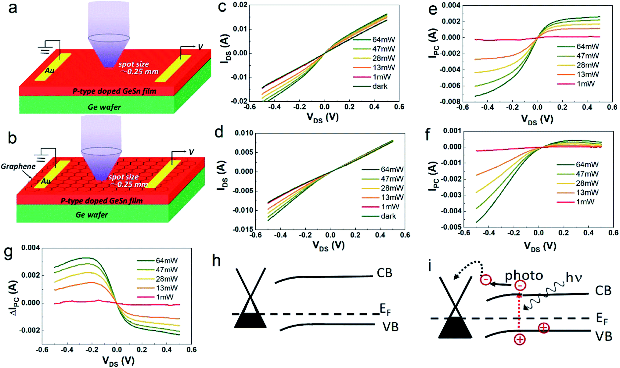 | ||
| Fig. 1 (a and b) Schematic of p-type doped-GeSn and graphene/p-type doped-GeSn heterostructure devices. (c and d) IDS–VDS characteristics and (e and f) IPC–VDS characteristics for p-type GeSn and graphene/p-type GeSn heterostructure under 1064 nm laser illumination respectively. (g) ΔIPC as a function of VDS. (h and i) Schematic of the band diagram of graphene/p-type GeSn system without and with laser illumination. | ||
Fig. 2a–d show IDS–VDS characteristics and IPC–VDS characteristics for devices with and without graphene on n-type GeSn under 1064 nm laser illumination. Interestingly, in contrast to the p-type GeSn, the photocurrents are enhanced by introducing a layer of graphene onto the n-type GeSn. Moreover, ΔIPC increases with laser power (Fig. 2e). In n-type GeSn, the Fermi energy is above the work function of monolayer graphene. The majority carriers (electrons) transfer into graphene or are trapped by the surface states, bending GeSn's energy-band upward at GeSn/graphene interface (Fig. 2f). Under laser illumination, holes in the GeSn layer can transit effectively into the graphene layer, which reduces the recombination in GeSn and results in an enhanced photocurrent. Moreover, in contrast to the graphene/p-type GeSn heterostructure, the photo-generated holes move into the graphene increasing the hole density in graphene and giving rise to the current enhancement shown in Fig. 2. Under a positive bias, ΔIPC is even greater than the IPC of bare n-type GeSn without graphene, suggesting that the integration of graphene can really separate and transport photo-generated carriers with higher efficiency.
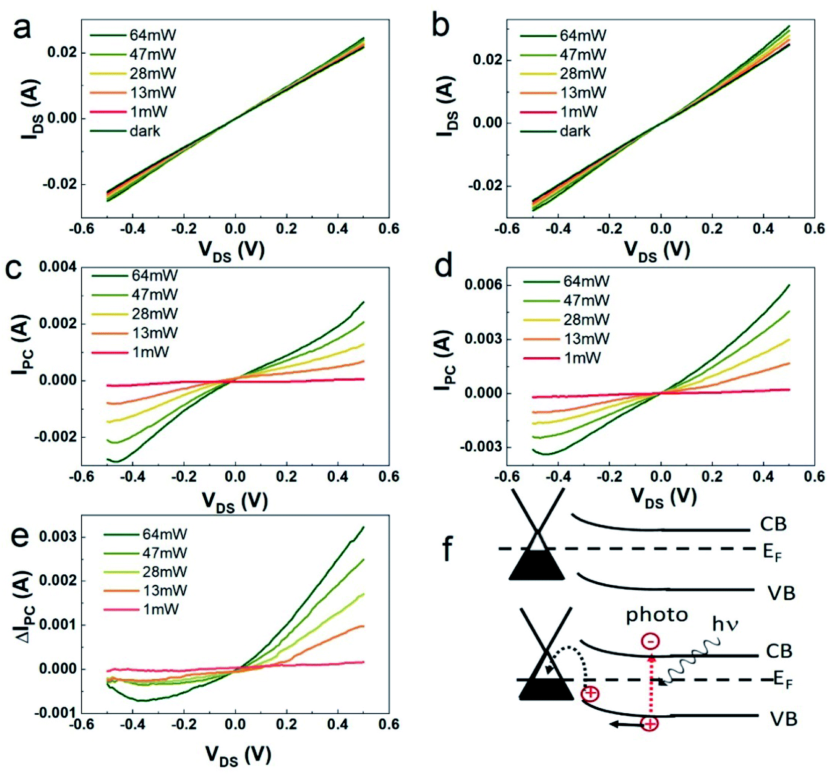 | ||
| Fig. 2 (a and b) IDS–VDS characteristics and (c and d) IPC–VDS characteristics for n-type GeSn and graphene/n-type GeSn heterostructure under 1064 nm laser illumination respectively. (e) ΔIPC as a function of VDS. (f) Schematic of the band diagram of graphene/n-type GeSn without and with laser illumination. | ||
Fig. 3a shows the photocurrents for the 4 different types of devices under a variety laser powers. The photocurrents increase with incident laser power and a photocurrent of 6 mA is achieved for graphene/n-type GeSn heterostructures. To demonstrate the performance of those 4 different device types, responsivity was also plotted (Fig. S4†), where the responsivity (R) is defined as R = IPC/P, where P is incident laser power density. In this work, the laser power density was measured using a commercial power meter. The responsivity of n-type GeSn is almost flat within the power range used in our experiments, but for the graphene/n-type GeSn heterostructures, the responsivity increases quickly with decreasing laser power and a responsivity of 200 mA W−1 is achieved with a laser power of 1 mW, which corresponds a power density of 2.037 W cm−2. Thus, graphene/n-type GeSn heterostructures are very promising for sensing weak signals.31 For photodetectors, the responsivity and incident laser power density usually follow the relationship R ∼ Pβ, where the exponent β conveys the superior photocurrent capability and the separation efficiency of the photo-induced charge carriers.32 To obtain β, log![[thin space (1/6-em)]](https://www.rsc.org/images/entities/char_2009.gif) R is plotted as a function of logP (Fig. 3b). For GeSn devices without graphene, β is almost zero under low incident powers. While for graphene/GeSn heterostructure devices, β is around −0.2 under low incident powers for graphene integrated with both types of GeSn, indicating that the additional graphene can really separate and transport a larger portion of photo-generated carriers. The separated photo-generated carriers increase the carrier density in the graphene layer for the graphene/n-type GeSn heterostructure devices but they recombine with carriers in the graphene layer for the graphene/p-type GeSn heterostructure devices. This is why photocurrents were suppressed in the graphene/p-type GeSn heterostructures but enhanced in the graphene/n-type GeSn heterostructures. Interestingly, for the graphene/p-type GeSn devices, β is negative at low incident power but positive at high incident power. This phenomenon is attributed to a photo-induced change in the bending profile. As shown in Fig. 1f, the band profile separates photo-generated electrons and holes. Due to the narrow band gap of GeSn, the bending profile is relatively small and decreases with density of minority carriers. Under high incident power, a high density of electron–hole pairs are generated, which flattens the bending profile. Both types of carriers can flow into the graphene layer creating not only an electron current but also a hole current. Moreover, more holes will be flow from GeSn into the graphene layer than electrons, since holes are majority carriers in the p-type GeSn, which increases the responsivity and results in a positive β.
R is plotted as a function of logP (Fig. 3b). For GeSn devices without graphene, β is almost zero under low incident powers. While for graphene/GeSn heterostructure devices, β is around −0.2 under low incident powers for graphene integrated with both types of GeSn, indicating that the additional graphene can really separate and transport a larger portion of photo-generated carriers. The separated photo-generated carriers increase the carrier density in the graphene layer for the graphene/n-type GeSn heterostructure devices but they recombine with carriers in the graphene layer for the graphene/p-type GeSn heterostructure devices. This is why photocurrents were suppressed in the graphene/p-type GeSn heterostructures but enhanced in the graphene/n-type GeSn heterostructures. Interestingly, for the graphene/p-type GeSn devices, β is negative at low incident power but positive at high incident power. This phenomenon is attributed to a photo-induced change in the bending profile. As shown in Fig. 1f, the band profile separates photo-generated electrons and holes. Due to the narrow band gap of GeSn, the bending profile is relatively small and decreases with density of minority carriers. Under high incident power, a high density of electron–hole pairs are generated, which flattens the bending profile. Both types of carriers can flow into the graphene layer creating not only an electron current but also a hole current. Moreover, more holes will be flow from GeSn into the graphene layer than electrons, since holes are majority carriers in the p-type GeSn, which increases the responsivity and results in a positive β.
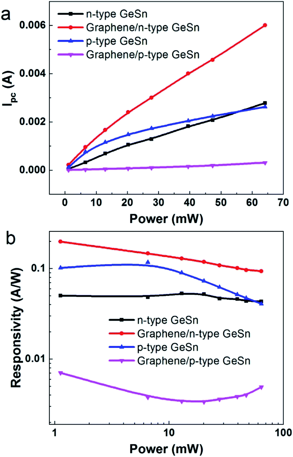 | ||
| Fig. 3 (a) IPC and (b) responsivity as a function of incident power under a bias voltage of 0.5 V. | ||
Fig. S5† shows the time response for each of the 4 device types. All the devices show fast photo responses with a quick activation in IPC when illuminated by the laser. When the devices are continuously illuminated with a high laser power density, the photocurrent for n-GeSn and graphene/p-type GeSn heterostructure devices gradually increase with time. While for p-type GeSn and graphene/p-type GeSn heterostructure devices, photocurrents gradually decrease. GeSn/Ge is a type-I heterostructure as plotted in Fig. S6.†33 Both photo-generated electrons and holes are confined in the GeSn layer for the n-type GeSn/n-type Ge heterostructure, resulting in a high recombination rate and leading to long response rise time. Meanwhile for the p-type GeSn/n-type Ge heterostructure photo-generated electrons and holes are separated by the band profile of the heterostructure. Thus, higher photocurrents are observed for the p-type GeSn/n-type the Ge heterostructure compared with the n-type GeSn/n-type Ge heterostructure when illuminated by the laser. Under high power laser illumination electrons in the Ge layer may transit to the GeSn, which decreases the photocurrents of the p-type GeSn based devices.
To prove the broadband detection capability from the visible to near infrared range, measurements under different incident wavelengths were performed. Fig. S7† shows the IDS of graphene/n-type GeSn heterostructures measured using an Omni-λ300i monochromator with a Zolix 150 W xenon light source. One can see that graphene/GeSn heterostructures can detect light with a wavelength up to 1832 nm. Fig. S8–S13† show the photoelectrical properties of GeSn and graphene/GeSn heterostructures under 532, 635, and 785 nm laser illuminations. It was found that the photocurrents were always enhanced for the graphene/n-type GeSn heterostructures but suppressed for the graphene/p-type GeSn heterostructures. Fig. 4 shows the enhancement in photocurrents under different incident wavelengths, where the enhancement factor is defined as the ratio between the performance of the heterostructure and the bare GeSn without graphene under the same conditions. An enhancement of 4 is achieved in graphene/n-type GeSn heterostructures under a 1064 nm laser illumination with a power of 1 mW. Interestingly, the enhancement (suppression) factor increases with laser wavelength. Under high energy laser illumination, both photo-generated electrons and holes can overcome the band profile and flow into the graphene, which reduces the charge separation efficiency.
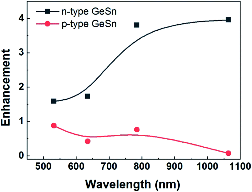 | ||
| Fig. 4 Enhancement factor of photocurrent for graphene/n-GeSn and graphene/p-GeSn under different excitation wavelength. | ||
Table 1 lists performance of photodetectors based on graphene integrated with a wide selection of conventional semiconductors. One finds that most of the graphene/Si photodetectors are reported to operate within the visible light band with a photoresponsivity of hundreds of mA W−1.34–39 For graphene/Ge hybrid systems, the detectors are usually optimized to function at wavelengths greater than 1200 nm but less than 1600 nm. Moreover, the responsivity is typically in the tens mA W−1 range.15,39,40 Graphene/GaAs based photodetectors can sense light from 325 to 1050 nm.41–46 Graphene/GeSn works well in the shortwave infrared range but its effectivity is suppressed in the visible or near infrared range. One can see that in these graphene based heterojunction photodetectors, optical absorption takes place in semiconductor side, while graphene only acts as a transparent electrode to collect carriers, which limits their photodetection capability. However, our graphene/n-type GeSn based photodetector has a responsivity of 200 mA W−1 and exhibits broadband photodetection from 532 nm to 1832 nm.
| Device structure | Spectral range | Responsivity | Ref. |
|---|---|---|---|
| Graphene/n-type Si | 400–900 nm | 225 mA W−1 (2.6 mW cm−2) | 34 |
| Graphene–Si | 850 nm | 29 mA W−1 (5 mW cm−2) | 35 |
| Graphene/Si | 410–950 nm | 730 mA W−1 (250 μW cm−2) | 36 |
| Graphene/Si | 1550 nm | 1.3 mA W−1 (0.73 mW cm−2); 39.5 mA W−1 (0.14 mW cm−2) | 37 |
| Graphene/Si | 532 nm | 510 mA W−1 (60 μW cm−2) | 38 |
| Graphene/Ge/Si | 45 mA W−1 (4.8 mW) | 39 | |
| Multi-layer graphene/n-type Ge | 1200–1600 nm | 51.8 mA W−1 | 15 |
| Graphene/Ge/SiO2 | 1550 nm | 62.1 mA W−1 (27 mW cm−2) | 40 |
| Graphene/GaAs | 405–850 nm | 122 mA W−1 (10 mW cm−2) | 41 |
| Nano particle/graphene/GaAs | 980 nm | 17.6 mA W−1 (19 mW cm−2) | 42 |
| Ag NPs/graphene/GaAs | 325–980 nm | 210 mA W−1 (43 μW) | 43 |
| Bilayer graphene/GaAs | 850 nm | 5 mA W−1 | 44 |
| GaAs/multi-layer graphene | 650–1050 nm | 1.73 mA W−1 | 45 |
| GaAs nanowire/graphene | 532 nm | 231 mA W−1 (0.393 μW) | 46 |
| Ge1−xSnx–graphene | 1064–2600 nm | 1968 A W−1 (29 nW) | 19 |
| Graphene/n-type GeSn | 532–1832 nm | 200 mA W−1 (1.125 mW); 3184.7 mA W−1 (1 nW) | This work |
Conclusions
In summary, we investigated the photoelectrical properties of doped GeSn with and without graphene layers. It is found that the photo-generated carriers can be separated and transported with higher efficiency by the addition of a graphene layer, and the laser power and the laser energy can affect the charge separation efficiency. Our experimental investigation suggests that photodetectors with high performance and broadband photodetection capability can be achieved by the integration of graphene with n-type GeSn. It may also inspire potential applications using graphene, GeSn, and graphene/GeSn heterostructures.47–50Conflicts of interest
There are no conflicts to declare.Acknowledgements
This work was supported by the National Key Research and Development Program under grant No. 2017YFE0301404 and 2017YFA0303800, the National Natural Science Foundation of China (No. 61874010 and 11804237), the Science and Technology Innovation Program for Creative Talents in Beijing Institute of Technology (No. 2017CX01006).References
- S. Gupta, B. Magyari-Kope, Y. Nishi and K. C. Saraswat, Achieving direct band gap in germanium through integration of Sn alloying and external strain, J. Appl. Phys., 2013, 113, 073707 CrossRef.
- A. C. Meng, C. S. Fenrich, M. R. Braun, J. P. McVittie, A. F. Marshall, J. S. Harris and P. C. McIntyre, Core-Shell Germanium/Germanium Tin Nanowires Exhibiting Room Temperature Direct- and Indirect-Gap Photoluminescence, Nano Lett., 2016, 16, 7521–7529 CrossRef CAS PubMed.
- R. Chen, S. Gupta, Y. C. Huang, Y. J. Huo, C. W. Rudy, E. Sanchez, Y. Kim, T. I. Kamins, K. C. Saraswat and J. S. Harris, Demonstration of a Ge/GeSn/Ge Quantum-Well Microdisk Resonator on Silicon: Enabling High-Quality Ge(Sn) Materials for Micro- and Nanophotonics, Nano Lett., 2014, 14, 37–43 CrossRef CAS PubMed.
- H. Cong, F. Yang, C. L. Xue, K. Yu, L. Zhou, N. Wang, B. W. Cheng and Q. M. Wang, Multilayer Graphene-GeSn Quantum Well Heterostructure SWIR Light Source, Small, 2018, 14, 1704414 CrossRef PubMed.
- C. Chang, H. Li, C. T. Ku, S. G. Yang, H. H. Cheng, J. Hendrickson, R. A. Soref and G. Sun, Ge0.975Sn0.025 320 × 256 imager chip for 1.6-1.9 μm infrared vision, Appl. Opt., 2016, 55, 10170–10173 CrossRef CAS PubMed.
- C. Chang, H. Li, S. H. Huang, H. H. Cheng, G. Sun and R. A. Soref, Sn-based Ge/Ge0.975Sn0.025/Ge p-i-n photodetector operated with back-side illumination, Appl. Phys. Lett., 2016, 108, 151101 CrossRef.
- K. S. Novoselov, A. K. Geim, S. V. Morozov, D. Jiang, Y. Zhang, S. V. Dubonos, I. V. Grigorieva and A. A. Firsov, Electric Field Effect in Atomically Thin Carbon Films, Science, 2004, 306, 666–669 CrossRef CAS PubMed.
- A. K. Geim and K. S. Novoselov, The rise of graphene, Nat. Mater., 2007, 6, 183–191 CrossRef CAS PubMed.
- S. K. Behura, C. Wang, Y. Wen and V. Berry, Graphene-semiconductor heterojunction sheds light on emerging photovoltaics, Nat. Photonics, 2019, 13, 312–318 CrossRef CAS.
- A. Di Bartolomeo, An experimental review of the rectifying graphene/semiconductor heterojunction, Phys. Rep., 2016, 606, 1–58 CrossRef CAS.
- X. M. Li and H. W. Zhu, The graphene-semiconductor Schottky junction, Phys. Today, 2016, 69, 47–51 Search PubMed.
- X. M. Li, Z. Lv and H. W. Zhu, Carbon/Silicon Heterojunction Solar Cells: State of the Art and Prospects, Adv. Mater., 2015, 27, 6549–6574 CrossRef CAS.
- C. C. Chen, M. Aykol, C. C. Chang, A. F. Levi and S. B. Cronin, Graphene-silicon Schottky diodes, Nano Lett., 2011, 11, 1863–1867 CrossRef CAS.
- X. M. Li, H. W. Zhu, K. L. Wang, A. Y. Cao, J. Q. Wei, C. Y. Li, Y. Jia, Z. Li, X. Li and D. H. Wu, Graphene-On-Silicon Schottky Junction Solar Cells, Adv. Mater., 2010, 22, 2743–2748 CrossRef CAS PubMed.
- L. H. Zeng, M. Z. Wang, H. Hu, B. Nie, Y. Q. Yu, C. Y. Wu, L. Wang, J. G. Hu, C. Xie, F. X. Liang and L. B. Luo, Monolayer graphene/germanium Schottky junction as high-performance self-driven infrared light photodetector, ACS Appl. Mater. Interfaces, 2013, 5, 9362–9366 CrossRef CAS PubMed.
- W. Jie, F. Zheng and J. Hao, Graphene/gallium arsenide-based Schottky junction solar cells, Appl. Phys. Lett., 2013, 103, 233111 CrossRef.
- H. Park, J. A. Rowehl, K. K. Kim, V. Bulovic and J. Kong, Doped graphene electrodes for organic solar cells, Nanotechnology, 2010, 21, 505204 CrossRef.
- R. Won, Graphene–silicon solar cells, Nat. Photonics, 2010, 4, 411 CrossRef CAS.
- F. Yang, K. Yu, H. Cong, C. Xue, B. Cheng, N. Wang, L. Zhou, Z. Liu and Q. Wang, Highly Enhanced SWIR Image Sensors Based on Ge1–xSnx–Graphene Heterostructure Photodetector, ACS Photonics, 2019, 6, 1199–1206 CrossRef CAS.
- H. Li, Y. X. Cui, K. Y. Wu, W. K. Tseng, H. H. Cheng and H. Chen, Strain relaxation and Sn segregation in GeSn epilayers under thermal treatment, Appl. Phys. Lett., 2013, 102, 251907 CrossRef.
- S. Chen, H. Ji, H. Chou, Q. Li, H. Li, J. W. Suk, R. Piner, L. Liao, W. Cai and R. S. Ruoff, Millimeter-Size Single-Crystal Graphene by Suppressing Evaporative Loss of Cu During Low Pressure Chemical Vapor Deposition, Adv. Mater., 2013, 25, 2062–2065 CrossRef CAS PubMed.
- X. Liu, D. Zhang, Y.-C. Wu, M. Yang, Q. Wang, C. O. Coileain, H. Xu, C. Yang, M. Abid, M. Abid, H. Liu, B. S. Chun, Q. Shi and H.-C. Wu, Ultra-sensitive graphene based mid-infrared plasmonic bio-chemical sensing using dielectric beads as a medium, Carbon, 2017, 122, 404–410 CrossRef CAS.
- H. F. Fei, G. Wu, W. Y. Cheng, W. J. Yan, H. Xu, D. Zhang, Y. F. Zhao, Y. H. Lv, Y. H. Chen, L. Zhang, C. O. Coileain, C. L. Heng, C. R. Chang and H. C. Wu, Enhanced NO2 Sensing at Room Temperature with Graphene via Monodisperse Polystyrene Bead Decoration, ACS Omega, 2019, 4, 3812–3819 CrossRef CAS.
- A. Gassenq, L. Milord, J. Aubin, N. Pauc, K. Guilloy, J. Rothman, D. Rouchon, A. Chelnokov, J. M. Hartmann, V. Reboud and V. Calvo, Raman spectral shift versus strain and composition in GeSn layers with 6%-15% Sn content, Appl. Phys. Lett., 2017, 110, 112101 CrossRef.
- C. Chang, H. Li, T. P. Chen, W. K. Tseng, H. Cheng, C. T. Ko, C. Y. Hsieh, M. J. Chen and G. Sun, The strain dependence of Ge(1-x)Sn(x) (x=0.083) Raman shift, Thin Solid Films, 2015, 593, 40–43 CrossRef CAS.
- Z. H. Ni, Y. Y. Wang, T. Yu and Z. X. Shen, Raman Spectroscopy and Imaging of Graphene, Nano Res., 2008, 1, 273–291 CrossRef CAS.
- Y. Y. Wang, Z. H. Ni, T. Yu, Z. X. Shen, H. M. Wang, Y. H. Wu, W. Chen and A. T. S. Wee, Raman studies of monolayer graphene: the substrate effect, J. Phys. Chem. C, 2008, 112, 10637–10640 CrossRef CAS.
- Y. M. Shi, K. K. Kim, A. Reina, M. Hofmann, L. J. Li and J. Kong, Work Function Engineering of Graphene Electrode via Chemical Doping, ACS Nano, 2010, 4, 2689–2694 CrossRef CAS PubMed.
- F. Schedin, A. K. Geim, S. V. Morozov, E. W. Hill, P. Blake, M. I. Katsnelson and K. S. Novoselov, Detection of individual gas molecules adsorbed on graphene, Nat. Mater., 2007, 6, 652–655 CrossRef CAS PubMed.
- M. Lafkioti, B. Krauss, T. Lohmann, U. Zschieschang, H. Klauk, K. V. Klitzing and J. H. Smet, Graphene on a Hydrophobic Substrate: Doping Reduction and Hysteresis Suppression under Ambient Conditions, Nano Lett., 2010, 10, 1149–1153 CrossRef CAS PubMed.
- H. Li, C. Chang, H. H. Cheng, G. Sun and R. A. Soref, Disorder-induced enhancement of indirect absorption in a GeSn photodetector grown by molecular beam epitaxy, Appl. Phys. Lett., 2016, 108, 191111 CrossRef.
- H. Xue, Y. Y. Dai, W. Kim, Y. D. Wang, X. Y. Bai, M. Qi, K. Halonen, H. Lipsanen and Z. P. Sun, High photoresponsivity and broadband photodetection with a band-engineered WSe2/SnSe2 heterostructure, Nanoscale, 2019, 11, 3240–3247 RSC.
- Y. Zhou, W. Dou, W. Du, T. Pham, S. A. Ghetmiri, S. Al-Kabi, A. Mosleh, M. Alher, J. Margetis, J. Tolle, G. Sun, R. Soref, B. Li, M. Mortazavi, H. Naseem and S.-Q. Yu, Systematic study of GeSn heterostructure-based light-emitting diodes towards mid-infrared applications, J. Appl. Phys., 2016, 120, 023102 CrossRef.
- X. H. An, F. Z. Liu, Y. J. Jung and S. Kar, Tunable Graphene-Silicon Heterojunctions for Ultrasensitive Photodetection, Nano Lett., 2013, 13(3), 909–916 CrossRef CAS PubMed.
- P. Lv, X. J. Zhang, X. Zhang, W. Deng and J. S. Jie, High-Sensitivity and Fast-Response Graphene/Crystalline Silicon Schottky Junction-Based Near-IR Photodetectors, IEEE Electron Device Lett., 2013, 34(10), 1337–1339 CAS.
- X. Li, M. Zhu, M. Du, Z. Lv, L. Zhang, Y. Li, Y. Yang, T. Yang, X. Li, K. Wang, H. Zhu and Y. Fang, High Detectivity Graphene-Silicon Heterojunction Photodetector, Small, 2016, 12(5), 595–601 CrossRef CAS PubMed.
- C. X. Wang, Y. Dong, Z. J. Lu, S. R. Chen, K. W. Xu, Y. M. Ma, G. B. Xu, X. Y. Zhao and Y. Q. Yu, High responsivity and high-speed 1.55 μm infrared photodetector from self-powered graphene/Si heterojunction, Sens. Actuators, A, 2019, 291, 87–92 CrossRef CAS.
- D. Periyanagounder, P. Gnanasekar, P. Varadhan, J. H. He and J. Kulandaivel, High performance, self-powered photodetectors based on a graphene/silicon Schottky junction diode, J. Mater. Chem. C, 2018, 6(35), 9545–9551 RSC.
- G. Niu, G. Capellini, G. Lupina, T. Niermann, M. Salvalaglio, A. Marzegalli, M. A. Schubert, P. Zaumseil, H. M. Krause, O. Skibitzki, M. Lehmann, F. Montalenti, Y. H. Xie and T. Schroeder, Photodetection in Hybrid Single-Layer Graphene/Fully Coherent Germanium Island Nanostructures Selectively Grown on Silicon Nanotip Patterns, ACS Appl. Mater. Interfaces, 2016, 8(3), 2017–2026 CrossRef CAS PubMed.
- A. Xu, S. W. Yang, Z. D. Liu, G. J. Li, J. R. Li, Y. Li, D. Chen, Q. L. Guo, G. Wang and G. Q. Ding, Near-infrared photodetector based on Schottky junctions of monolayer graphene/GeOI, Mater. Lett., 2018, 227, 17–20 CrossRef CAS.
- Z. Tao, D. Zhou, H. Yin, B. F. Cai, T. T. Huo, Ju. Ma, Z. F. Di, N. T. Hu, Z. Yang and Y. J. Su, Graphene/GaAs heterojunction for highly sensitive, self-powered Visible/NIR photodetectors, Mater. Sci. Semicond. Process., 2020, 111, 104989 CrossRef CAS.
- J. Wu, Z. Yang, C. Qiu, Y. Zhang, Z. Wu, J. Yang, Y. Lu, J. Li, D. Yang, R. Hao, E. Li, G. Yu and S. Lin, Enhanced performance of a graphene/GaAs self-driven near-infrared photodetector with upconversion nanoparticles, Nanoscale, 2018, 10(17), 8023–8030 RSC.
- Y. H. Lu, S. R. Feng, Z. Q. Wu, Y. X. Gao, J. L. Yang, Y. J. Zhang, Z. Z. Hao, J. F. Li, E. P. Li, H. S. Chen and S. S. Lin, Broadband surface plasmon resonance enhanced self-powered graphene/GaAs photodetector with ultrahigh detectivity, Nano Energy, 2018, 47, 140–149 CrossRef CAS.
- L.-B. Luo, H. Hu, X.-H. Wang, R. Lu, Y.-F. Zou, Y.-Q. Yu and F.-X. Liang, A graphene/GaAs near-infrared photodetector enabled by interfacial passivation with fast response and high sensitivity, J. Mater. Chem. C, 2015, 3(18), 4723–4728 RSC.
- L.-B. Luo, J.-J. Chen, M.-Z. Wang, H. Hu, C.-Y. Wu, Q. Li, L. Wang, J.-A. Huang and F.-X. Liang, Near-Infrared Light Photovoltaic Detector Based on GaAs Nanocone Array/Monolayer Graphene Schottky Junction, Adv. Funct. Mater., 2014, 24(19), 2794–2800 CrossRef CAS.
- Y. Luo, X. Yan, J. Zhang, B. Li, Y. Wu, Q. Lu, C. Jin, X. Zhang and X. Ren, A graphene/single GaAs nanowire Schottky junction photovoltaic device, Nanoscale, 2018, 10(19), 9212–9217 RSC.
- J. Teng, L. Shen, Y. Xu, Y. Chen, X. L. Wu, Y. He, J. Chen and H. Lin, Effects of molecular weight distribution of soluble microbial products (SMPs) on membrane fouling in a membrane bioreactor (MBR): Novel mechanistic insights, Chemosphere, 2020, 248, 126013 CrossRef CAS PubMed.
- W. Yu, Y. Liu, L. Shen, Y. Xu, R. Li, T. Sun and H. Lin, Magnetic field assisted preparation of PES-Ni@MWCNTs membrane with enhanced permeability and antifouling performance, Chemosphere, 2020, 243, 125446 CrossRef CAS PubMed.
- W. Yu, Y. Liu, Y. Xu, R. Li, J. Chen, B.-Q. Liao, L. Shen and H. Lin, A conductive PVDF-Ni membrane with superior rejection, permeance and antifouling ability via electric assisted in-situ aeration for dye separation, J. Membr. Sci., 2019, 581, 401–412 CrossRef CAS.
- M. Wu, Y. Chen, H. Lin, L. Zhao, L. Shen, R. Li, Y. Xu, H. Hong and Y. He, Membrane fouling caused by biological foams in a submerged membrane bioreactor: mechanism insights, Water Res., 2020, 181, 115932 CrossRef CAS PubMed.
Footnote |
| † Electronic supplementary information (ESI) available. See DOI: 10.1039/d0ra04308g |
| This journal is © The Royal Society of Chemistry 2020 |