
 Open Access Article
 This Open Access Article is licensed under a Creative Commons Attribution-Non Commercial 3.0 Unported Licence
A simple multiple centrifugation method for large-area homogeneous perovskite CsPbBr3 films with optical lasing†
Chang-Gui Lu‡
*,
Xue-Fang Hu‡,
Shu-Hong Xu ,
Hong-Gui Liu,
Jing-Kun Xu,
Yi-Ping Cui and
Chun-Lei Wang*
,
Hong-Gui Liu,
Jing-Kun Xu,
Yi-Ping Cui and
Chun-Lei Wang*
Advanced Photonics Center, School of Electronic Science & Engineering, Southeast University, Nanjing, Jiangsu 210096, China. E-mail: changguilu@seu.edu.cn; wangchl@seu.edu.cn
First published on 6th July 2020
Abstract
Large scale cesium lead-halide (CsPbX3, X = Cl, Br, and I) perovskite films have become the basis of laser applications. Common fabrication methods such as spin-coating and thermal evaporation have a trade-off between high quality and low cost. Herein, we reported a facile method for preparing a large area homogeneous perovskite CsPbBr3 film via a multiple centrifugal deposition and solvent annealing (MCDSA) method. This method is superior because it can control the thickness (180 nm to 880 nm) of the film, ensure the film is crack and pinhole free, has a large area (2.5 cm × 2.5 cm), and has a low surface roughness (a root mean square of 32 nm). Multiple times of centrifugation and solvent annealing in the MCDSA method are key to improving the quality of the film as well as the laser performance. With increased centrifugation cycles from one to four, the thickness of the film increases from 180 nm to 880 nm, leading to a decrease in the laser threshold from 18.1 μJ cm−2 to 14.2 μJ cm−2 and an increase in the gain coefficient from 78.5 cm−1 to 112.7 cm−1. When solvent annealing is employed, the gain coefficient is further increased to 122.7 cm−1.
1 Introduction
Recently, all-inorganic cesium lead-halide (CsPbX3, X = Cl, Br, and I) perovskite films have grown in popularity due to their superior optical properties such as high photoluminescence quantum yields (PLQYs),1,2 narrow emission line widths,3,4 wide emission spectra tunability,5–7 and low material costs.8,9 These properties make them a prime candidate for use in solar cells,10–12 white light-emitting diodes,13–15 displays,16 photodetectors,17,18 laser and so on.19–21 The fabrication of high quality CsPbX3 perovskite films is a prerequisite for numerous applications. For example in laser applications, perovskite films act as the gain medium and the resonant cavity. The film quality, including its smoothness, the homogeneousness of its large area, and thickness, are fundamental for realizing low threshold and high gain coefficients.There are numerous ways to fabricate CsPbBr3 films. The most common methods are spin-coating and thermal evaporation. Spin-coating is a facile preparation approach, which is achieved by dropping a CsPbBr3 solution onto the substrate while rotating at a high speed. Thus, making this method very easy to operate. The as-prepared CsPbBr3 films usually result in inhomogeneous samples (having numerous cracks and uncovered pin-holes) with relatively large surface roughness. Moreover, this method wastes a serious amount of material, almost 99% of the source is out of use, making it unsuitable for mass production. Since spin-coating does not deposit compact and homogeneous films with large areas, numerous post-treatments are necessary to improve the morphology and crystallinity of the films.22–25 Thermal evaporation is another effective way to fabricate large-scale CsPbBr3 films. In this method, the source material is placed in an evaporator and the high temperature deposits the source material on the substrate, making the film compact and homogeneous over a large area. In comparison to spin-coating, the thermal evaporation method can produce CsPbBr3 films with better crystalline qualities, lower defect densities, and highly flat and smooth surfaces. In particular, thermal evaporation has shown great success in creating high-quality nanostructures with controllable thickness. However, the synthesis process is complicated and requires dedicated equipment. Designated experimental conditions are also needed, leading to increased costs of the films.26–30 Overall, both spin-coating and thermal evaporation do not satisfy the requirement of high quality and low cost simultaneously. Thus, it is highly desirable to develop a new method that aims to produce CsPbBr3 films with good surface characteristics in an inexpensive manner.
In this study, we develop a multiple centrifugal deposition and solvent annealing (MCDSA) method for the large scale fabrication of CsPbBr3 films with low surface roughness, low cost and good stability.31–34 By changing the repetition times of the centrifugation process, the thickness of the CsPbBr3 films can be controlled. Due to the high quality of the films, with a low surface roughness (root mean square of 32 nm) and a large area (2.5 cm × 2.5 cm), the as-prepared CsPbBr3 films show good laser performance. The measured ASE threshold and the gain coefficient are 14.2 μJ cm−2 and 122.7 cm−1, respectively. We note the recent report of colloidal quantum dot films fabricated using a centrifugal casting method.35,36 Though the films are crack-free and macroscopically uniform over large areas, the films are thin, making them only suitable for photodetector rather than laser applications. Thus, this work is the first report of a simple preparation and low cost method for obtaining CsPbBr3 films with large area homogeneity, a low laser threshold, and a high gain coefficient, which has promising applications in the optical lasing field.
2 Results and discussion
2.1 Preparation of CsPbBr3 films
Fig. 1 illustrates the typical MCDSA method, which includes three steps: (1) the preparation of CsPbBr3 quantum dots (QDs) by mixing toluene with a dimethylsulfoxide (DMSO) solution containing oleic acid (OA), oleylamine (OAm), CsBr, and PbBr2; (2) multiple times of centrifugation by putting the substrate in a freshly prepared CsPbBr3 QD solution; (3) solvent-gas atmosphere annealing by putting the substrate in a closed cuvette surrounded by alcohol and toluene vapors (see details in the ESI†). | ||
| Fig. 1 The flow diagram of the MCDSA method. | ||
X-ray diffraction (XRD) of the CsPbBr3 perovskite film in N2 atmosphere was recorded and is shown in Fig. 2(a). The strong intensity of the diffraction peaks indicates the good crystallinity of the film. Most of the peaks are in agreement with the standard (rhombic) CsPbBr3 (PDF#18-0364). The XRD pattern of the CsPbBr3 perovskite film in an air atmosphere was also measured. The presence of PbBr2 proved that an incomplete reaction occurred during the fabrication process (Table S2 in ESI†). A stability test conducted on the PL intensity indicated that the PL intensity is stable if stored in a N2 atmosphere rather than an air atmosphere (Table S3 in ESI†). The X-ray photoelectron spectroscopy (XPS) results shown in Fig. 2(b)–(d) display typical Cs peaks at 724.3 and 738.2 eV, Pb peaks at 137.9 and 142.7 eV and the Br peaks at 67.7 and 68.8 eV. From the SEM image in Fig. 2(e), we can see that the film is homogeneous and compact over a large area. No pinholes can be found. The absorption/photoluminescence (PL) spectrum of the CsPbBr3 films (Fig. 2(f)) displays an obvious peak at 516/529 nm, which is similar to that of the CsPbBr3 QD solution shown in Fig. S1 in the ESI.†
 | ||
| Fig. 2 (a) The XRD pattern of the CsPbBr3 film. (b) High-resolution XPS spectra of Cs3d, (c) Pb4f, and (d) Br3d. (e) SEM image. (f) The PL intensity and absorption of the CsPbBr3 film. | ||
One advantage of the MCDSA method is its ability to control the thickness of the film simply by changing the number of centrifugation steps. Three samples (labeled SA, SB, and SC) were fabricated using the MCDSA method with repetition numbers of one, two, and four, respectively. The centrifuge time and speed were kept constant as 2 minutes and 8500 rpm. The thicknesses of the films were measured via atomic force microscopy (AFM), as shown in Fig. 3.37 For samples SA, SB, and SC, the measured thicknesses were 180, 500, and 880 nm, respectively, confirming the effective control of the film thickness using the number of centrifugation cycles.
 | ||
| Fig. 3 The AFM pattern of the CsPbBr3 films (a) SA, (b) SB, and (c) SC. | ||
Another advantage of the MCDSA method is the superiority of the surface morphology film. As shown in Fig. 4(b), the film obtained using the MCDSA method is a smooth CsPbBr3 film with root mean square (RMS) of 32 nm. The third step of the MCDSA method, namely solvent-gas atmosphere annealing, is believed to be key for the formation of a smooth film. In a control experiment, the CsPbBr3 films were annealed directly without a solvent-gas atmosphere (sample SA). The resulting film showed pinholes and cracks and had an increased RMS of 37.8 nm, as shown in Fig. 4(a). It is well known that polar solvents play an important role in the dissolution and recrystallization of halide perovskites.38 A polar solvent-gas atmosphere can partially dissolve the surface of the film, followed by the recrystallization of the perovskite to reveal a more compact, smooth, and uniform surface.
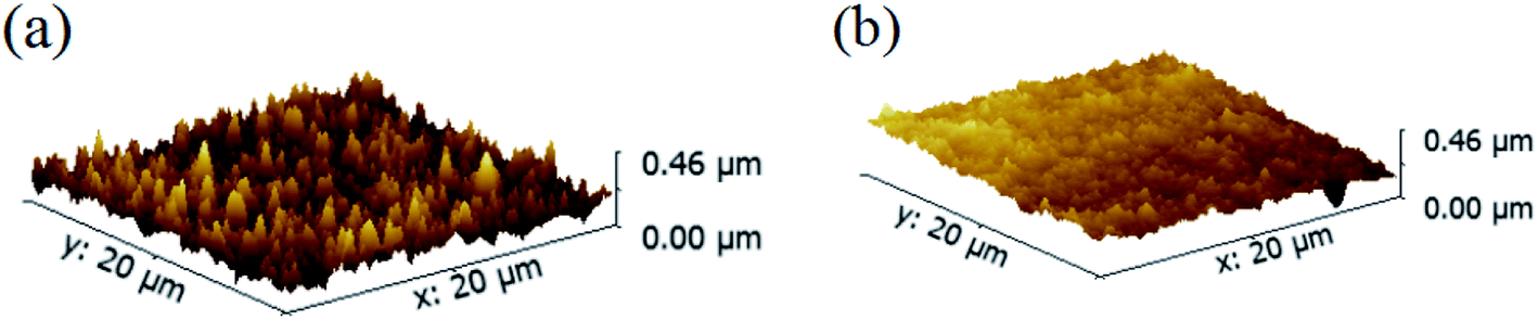 | ||
| Fig. 4 The AFM pattern of the CsPbBr3 film SA (a) direct annealing (b) solvent annealing. | ||
2.2 Laser measurement
A schematic of the ASE measurement is illustrated in Fig. 5. The excitation source used for this work was a Ti:sapphire oscillator/amplifier. The latter produced a ∼120 fs duration and had an 800 nm wavelength laser output with a repetition rate of 1 kHz. The output divergence angle after collimation is approximately 0.65 mrad. Using a beta barium borate (BBO) crystal, the output wavelength is converted to 400 nm. The pump beam is focused by a cylindrical lens on the sample, while the ASE signal is collected by a lens to the spectrograph. | ||
| Fig. 5 The schematic of the ASE measurement. | ||
The ASE property of the CsPbBr3 films (Fig. 6) depicted that the CsPbBr3 films under a low pump power present a broad spontaneous emission (SE) with a peak centered at 529 nm. With increasing pump density, a peak located at 536 nm emerges and quickly becomes dominant. Meanwhile, the FWHM of the emission spectrum narrows sharply, which signifies the transition from an SE process into the ASE regime. The measured emission spectra of the SD (about 880 nm without solvent annealing) and SC (about 880 nm with solvent annealing) samples, are shown in Fig. 6(a) and (b), respectively. It can be found that the intensity of the ASE signal is enhanced distinctly under the same pump intensity after solvent annealing (Table S1 in the ESI†). The threshold is decreased from 16.2 μJ cm−2 to 14.1 μJ cm−2. Moreover, the gain coefficient is increased from 112.7 cm−1 to 122.7 cm−1, suggesting that solvent annealing can slightly improve the gain coefficient of the CsPbBr3 film. A possible reason for the effect of solvent annealing is the improved surface morphology, which decreases the surface scattering of the film, thus decreasing the threshold and increasing the gain coefficient. The emission spectra of the SA (about 180 nm with solvent annealing) and SB (about 500 nm with solvent annealing) samples are shown in Fig. 6(c) and (d). Compared to Fig. 6(c) and (d) with Fig. 6(b), it is obvious that with the increase in the thickness from 180 nm to 880 nm, the intensity of the ASE increases. As a result, the threshold decreases from 18.1 μJ cm−2 to 14.2 μJ cm−2, and the gain coefficient increases from 78.5 cm−1 to 122.7 cm−1, as shown in Table S2 (ESI†). By comparing Tables S1 and S2 in the ESI,† it can be found that the thickness rather than solvent annealing is the dominant factor that affects the threshold and gain coefficient.
 | ||
| Fig. 6 The PL spectra of the (a) SD, (b) SC, (c) SA, and (d) SB samples. | ||
Fig. 7(a) shows the plot of the ASE intensity versus the intensity of the pump laser of the SC sample. Only spontaneous emission occurs under low pump intensity. When the pump intensity increases beyond the threshold, the emission intensity rises rapidly. The threshold of the film is 14.2 μJ cm−2, and the full width at half maximum (FWHM) is 28 nm when the pulse energy is 9.4 μJ cm−2. By further increasing the pulse energy to 45.5 μJ cm−2, the emission FWHM of the CsPbBr3 film decreases to 6 nm. The gain coefficient, a key factor of the gain medium, was measured as 122.7 cm−1 by changing the length of the slit, as depicted in Fig. 7(b). The output intensity shows an“S” shape with an increased excitation length. When the stripe length reaches the threshold value where propagation losses are compensated by optical amplification, the PL spectrum starts to show an additional ASE component that increases with the strip length. This is the reason why the output intensity at extremely large stripe lengths will deviate from the first six data.39,40 The plots of the ASE intensities versus the intensity of the pump laser of the SA, SB, and SD samples are also shown in Fig. S2 (ESI†). It can be concluded that the ASE behavior can be optimized greatly through increasing the thickness of the film or performing a solvent annealing treatment.
 | ||
| Fig. 7 (a) The ASE intensity of the SC sample versus the intensity of the pump laser. (b) The PL intensity of the SC sample versus the excitation length. | ||
We measured the emission lifetime using a streak camera (c5680-04/M, Hamamatsu). Fig. 8(a) shows the PL lifetime of the concentrated CsPbBr3 QD solution. The PL lifetime of the CsPbBr3 QD solution contains 4.00 ns and 46.85 ns, which was fitted by a double-exponential function. Fig. 8(b) and (c) show the time domain spectra of the SC sample. When the pump intensity increased from 10.7 μJ cm−2 to 25.0 μJ cm−2, the measured PL lifetime decreased from 0.37 ns to 0.14 ns. This was caused by the increased proportion of the ASE signal from 55% to 90% due to the increased stimulated radiation probability. The time-resolved PL spectra are shown in Fig. S3 (ESI†).
 | ||
| Fig. 8 The time resolution of the PL spectrum of the solution (a). The time resolution of the PL spectra of the film with the pump intensities of (b) 10.7 μJ cm−2 and (c) 25.0 μJ cm−2. | ||
3 Conclusions
In conclusion, we reported a simple MCDSA method for the preparation of large area homogeneous perovskite CsPbBr3 films using multiple centrifugation cycle deposition and solvent annealing techniques. This method can prepare CsPbBr3 films with a controllable thickness from 180 nm to 880 nm, large area (2.5 cm × 2.5 cm), and low surface roughness (a root mean square is 32 nm). By comparing three samples with different thicknesses (180 nm, 500 nm, and 880 nm), it was shown that the threshold decreased from 18.1 μJ cm−2 to 14.2 μJ cm−2 and the gain coefficient increased from 78.5 cm−1 to 122.7 cm−1 with increasing thickness. By comparing a solvent annealed sample to a sample that did not undergo solvent annealing, it was shown that the threshold decreased from 16.2 μJ cm−2 to 14.2 μJ cm−2, while the gain coefficient increased from 112.7 cm−1 to 122.7 cm−1. The results demonstrated that the threshold and the gain factor parameters can be optimized greatly through increasing the thickness of the sample and performing solvent annealing treatments.Conflicts of interest
There are no conflicts to declare.Acknowledgements
The work was financially supported by National Nature Science Foundation of China (11874107, 61875037, and 21875034).References
- J. H. Li, L. Xu, T. Wang, J. Song, J. Chen, J. Xue, Y. H. Dong, B. Cai, Q. S. Shan, B. N. Han and H. B. Zeng, Adv. Mater., 2017, 29, 1603885 CrossRef PubMed.
- W. Song, Y. C. Yang, X. J. Kang, L. Wang, L. J. Huang and D. C. Pan, Chem. Commun., 2016, 52, 7265–7268 RSC.
- H. R. Wang, X. Y. Zhang, Q. Q. Wu, F. Cao, D. W. Yang, Y. Q. Shang, Z. J. Ning, W. Zhang, W. T. Zheng, Y. F. Yan, S. V. Kershaw, L. J. Zhang, A. L. Rogach and X. Y. Yang, Nat. Commun., 2019, 10, 665 CrossRef CAS PubMed.
- X. Y. Zhang, H. Lin, H. Huang, C. Reckmeier, Y. Zhang, W. C. Choy and A. L. Rogach, Nano Lett., 2016, 16, 1415–1420 CrossRef CAS PubMed.
- Q. A. Akkerman, V. D'Innocenzo, S. Accornero, A. Scarpellini, A. Petrozza, M. Prato and L. Manna, J. Am. Chem. Soc., 2015, 137, 10276–10281 CrossRef CAS PubMed.
- L. F. Lv, Y. B. Xu, H. H. Fang, W. J. Luo, F. J. Xu, L. M. Liu, B. W. Wang, X. F. Zhang, D. Yang, W. D. Hu and A. G. Dong, Nanoscale, 2016, 8, 13589–13596 RSC.
- P. Ramasamy, D. H. Lim, B. Kim, S. H. Lee, M. S. Lee and J. S. Lee, Chem. Commun., 2016, 52, 2067–2070 RSC.
- C. Sun, Y. Zhang, C. Ruan, C. Y. Yin, X. Y. Wang, Y. D. Wang and W. W. Yu, Adv. Mater., 2016, 28, 10088–10094 CrossRef CAS PubMed.
- J. Z. Song, T. Fang, J. H. Li, L. M. Xu, F. J. Zhang, B. M. Han, Q. S. Shan and H. B. Zeng, Adv. Mater., 2018, 30, 1805409 CrossRef PubMed.
- H. Wang, Y. Wu, M. Ma, S. Dong, Q. Li, G. Du, H. Zhang and Q. Y. Xu, ACS Appl. Energy Mater., 2019, 2, 2305–2312 CrossRef CAS.
- J. Liang, C. X. Wang, Y. R. Wang, Z. R. Xu, Z. P. Lu, Y. Ma, H. F. Zhu, Y. Hu, C. C. Xiao, X. Yi, G. Y. Zhu, H. L. Lv, L. B. Ma, T. Chen, Z. X. Tie, Z. Jin and J. Liu, J. Am. Chem. Soc., 2016, 138, 15829–15832 CrossRef CAS PubMed.
- J. Z. Chen and N. G. Park, J. Phys. Chem. C, 2018, 122, 14039–14063 CrossRef CAS.
- J. Ma, H. Wu, J. B. Qiu, J. Wang, Q. Wang, Y. Yang, D. C. Zhou and J. Han, J. Phys. Chem. C, 2019, 31, 1936–1940 Search PubMed.
- Z. H. Wu, J. Wei, Y. N. Sun, J. Wu, Y. F. Hou, P. Wang, N. P. Wang and Z. F. Zhao, J. Mater. Sci., 2019, 54, 6917–6929 CrossRef.
- Y. S. Tan, Y. T. Zou, L. Z. Wu, Q. Huang, D. Yang, M. Chen, M. Y. Ban, C. Wu, T. Wu, S. Bai, T. Song, Q. Zhang and B. Q. Sun, ACS Appl. Mater. Interfaces, 2018, 10, 3784–3792 CrossRef CAS PubMed.
- Y. S. Tan, R. Y. Li, H. Xu, Y. S. Qin, T. Song and B. Q. Sun, Adv. Funct. Mater., 2019, 29, 1900730 CrossRef.
- R. H. Liu, H. Zhou, Z. N. Song, X. H. Yang, D. J. Wu, Z. H. Song, H. Wang and Y. F. Yan, Nanoscale, 2019, 11, 9302–9309 RSC.
- L. F. Lv, Y. B. Xu, H. H. Fang, W. J. Luo, F. J. Xu, L. M. Liu, B. W. Wang, X. F. Zhang, D. Yang, W. D. Hu and A. G. Dong, Nanoscale, 2016, 8, 13589–13596 RSC.
- Y. P. Fu, H. M. Zhu, C. S. Constantinos, Q. Ding, J. Wang, G. K. Mercouri, X. Y. Zhu and J. Song, ACS Nano, 2016, 10, 7963–7972 CrossRef CAS PubMed.
- J. Pan, P. S. Smritakshi, M. Banavoth, D. Ibrahim, W. Peng, R. P. Manas, J. K. Liu, L. F. Sinatra, N. T. Alyami, C. Zhao, E. Alarousu, T. K. Ng, S. O. Boon, M. B. Osman and F. M. Omar, J. Phys. Chem. Lett., 2015, 6, 5027–5033 CrossRef CAS PubMed.
- Y. Wang, X. M. Li, J. Z. Song, L. Xiao, H. B. Zeng and H. D. Sun, Adv. Mater., 2015, 27, 7101–7108 CrossRef CAS PubMed.
- B. Conings, L. Baeten, C. D. Dobbelaere, J. D'Haen, J. Manca and H. G. Boyen, Adv. Mater., 2014, 26, 2041–2046 CrossRef CAS PubMed.
- M. D. Xiao, F. Z. Huang, W. C. Huang, Y. Dkhissi, Y. Zhu, J. Etheridge, G. W. Angus, U. Bach, Y. B. Cheng and L. Spiccia, Angew. Chem., 2014, 126, 10056–10061 CrossRef.
- N. J. Jeon, J. H. Noh, Y. C. Kim, W. S. Yang, S. C. Ryu and S. Seok, Nat. Mater., 2014, 13, 897–903 CrossRef CAS PubMed.
- Y. C. Ling, Y. Tian, X. Wang, M. K. Javon, P. O. Fernando, Y. J. Du, L. Tan, K. Hanson, B. W. Ma and H. W. Gao, Adv. Mater., 2016, 28, 8983–8989 CrossRef CAS PubMed.
- Y. K. Chih, J. C. Wang, R. T. Yang, C. C. Liu, Y. C. Chang, Y. S. Fu, W. C. Lai, P. Chen, T. C. Wen, Y. C. Huang, C. S. Tsao and T. F. Guo, Adv. Mater., 2016, 28, 8687–8694 CrossRef CAS PubMed.
- J. Chen, Y. P. Fu, L. Samad, L. Dang, Y. Z. Zhao, S. H. Shen, L. J. Guo and J. Song, Nano Lett., 2017, 17, 460–466 CrossRef CAS PubMed.
- M. Z. Liu, M. B. Johnston and H. J. Snaith, Nature, 2013, 501, 395–398 CrossRef CAS PubMed.
- J. Chen, D. J. Morrow, Y. P. Fu, W. H. Zheng, Y. Z. Zhao, L. Dang, M. J. Stolt, D. D. Kohler, X. X. Wang, K. J. Czech, M. P. Hautzinger, S. H. Shen, L. J. Guo, A. L. Pan, J. C. Wright and J. Song, J. Am. Chem. Soc., 2017, 139, 13525–13532 CrossRef CAS PubMed.
- Y. C. Ling, L. Tan, X. Wang, Y. Zhou, Y. Xin, B. W. Ma, K. Hanson and H. W. Gao, J. Phys. Chem. Lett., 2017, 8, 3266–3271 CrossRef CAS PubMed.
- L. Ji, X. Z. Zhang, T. Zhang, Y. F. Wang, F. Wang, Z. Q. Zhong, Z. D. Chen, Z. W. Xiao, L. Chen and S. B. Li, J. Mater. Chem. A, 2019, 7, 9154 RSC.
- F. Wang, T. Zhang, Y. F. Wang, D. T. Liu, P. Zhang, H. Chen, L. Ji, L. Chen, Z. D. Chen, J. Wu, X. Liu, Y. B. Li, Y. F. Wang and S. B. Li, J. Mater. Chem. A, 2019, 7, 12166 RSC.
- P. Zhang, T. Zhang, Y. F. Wang, D. T. Liu, H. Xu, L. Chen, Y. B. Li, J. Wu, Z. D. Chen and S. B. Li, J. Power Sources, 2019, 439, 227091 CrossRef CAS.
- D. Liu, H. L. Zheng, L. Ji, H. Chen, Y. F. Wang, P. Zhang, F. Wang, J. Wu, Z. Chen and S. B. Li, J. Power Sources, 2019, 441, 227161 CrossRef CAS.
- Y. Kim, E. Yassitepe, C. Riccardo, G. Walters, X. W. Gong, P. Kanjianaboos, A. F. Nogueira and E. H. Sargent, ACS Appl. Mater. Interfaces, 2015, 7, 25007–25013 CrossRef CAS PubMed.
- J. Y. Kim, V. Adinolfi, B. R. Sutherland, O. Voznyy, S. J. Kwon, T. W. Kim, J. Kim, H. Ihee, K. Kemp, M. Adachi, M. J. Yuan, L. kramar, D. Zhitomirsky, S. Hoogland and E. H. Sargent, Nat. Commun., 2015, 6, 7772 CrossRef PubMed.
- S. B. Sun, D. Yuan, Y. Xu, A. F. Wang and Zh. T. Deng, ACS Nano, 2016, 10, 3648–3657 CrossRef CAS PubMed.
- X. M. Li, D. J. Yu, F. Cao, Y. Gu, Y. Wei, Y. Wu, J. Z. Song and H. B. Zeng, Adv. Funct. Mater., 2016, 26, 5903–5912 CrossRef CAS.
- P. Liu, X. X. He, J. H. Ren, Q. Liao, J. N. Yao and H. B. Fu, ACS Nano, 2017, 11, 5766–5773 CrossRef CAS PubMed.
- S. Yakunin, L. Protesescu, F. Krieg, M. I. Bodnarchuk, G. Nedelcu, M. Humer, G. D. Luca, M. Fiebig, W. Heiss and M. V. Kovalenko, Nat. Commun., 2015, 6, 8056 CrossRef CAS PubMed.
Footnotes |
| † Electronic supplementary information (ESI) available. See DOI: 10.1039/d0ra04259e |
| ‡ These authors contributed equally to this work. |
| This journal is © The Royal Society of Chemistry 2020 |