
 Open Access Article
 This Open Access Article is licensed under a Creative Commons Attribution-Non Commercial 3.0 Unported Licence
Understanding the effects of shape, material and location of incorporation of metal nanoparticles on the performance of plasmonic organic solar cells†
Minu Mohan,
Ramkumar Sekar and
Manoj A. G. Namboothiry *
*
School of Physics, Indian Institute of Science Education and Research Thiruvananthapuram (IISER-TVM), Maruthamala P O, Vithura, Thiruvananthapuram, Kerala 695551, India. E-mail: manoj@iisertvm.ac.in
First published on 10th July 2020
Abstract
Truncated octahedral gold (Au) nanoparticles (NPs), Au nanocubes (NCs)-, and silver (Ag) NCs are used to study the effect of NPs shape, material and incorporation location on the performance of poly(3-hexylthiophene):[6,6]-phenyl-C71-butyric acid methyl ester (P3HT:PC71BM) based inverted bulk heterojunction (BHJ) organic solar cells (OSCs). Plasmonic OSCs (POSCs) with NPs incorporated as an interfacial layer between zinc oxide (ZnO) and active layer showed highest power conversion efficiency (PCE) and short circuit current density (Jsc) values for all kind of shapes and material compared to POSCs with NPs blended into the active layer. Near-field enhancement as well as enhanced forward scattering cross section is attributed for POSC performance improvement. Among the NPs with two shapes, POSCs with truncated octahedral Au NPs exceeded the photovoltaic performance compared to those of POSCs with Au and Ag NCs. Large number of antennas in truncated octahedral Au NPs compared to NC is reasoned to be the cause for this improvement. Even though Ag has better localised surface plasmon resoanance (LSPR) properties compared to Au, the POSCs with Ag NCs showed lower Jsc value and is due to reduced number of photons at the blue shifted LSPR wavelength of Ag NCs. The improvement in Jsc values of POSCs is confirmed by enhancement in absorption, external quantum efficiency (EQE), exciton generation and exciton dissociation probability measurements and is due to improved LSPR coupling of the NPs with the active layer. The surface enhanced Raman scattering (SERS) and photoluminescence (PL) studies confirm the absorption enhancement in the active layer by NP LSPR coupling and further confirm the enhancement in the photovoltaic performance of POSCs.
Introduction
Photovoltaic research based on organic semiconductors has made remarkable progress during the last two decades.1,2 The improvement was mostly due to the development of new materials, interface engineering and modification in device architecture based on understanding of basic process involved in the photovoltaic performances.3,4 Some of the crucial basic processes addressed by various research groups are (1) absorption of light, (2) exciton generation, diffusion and dissociation, (3) free charge carrier transport and (4) free carrier extraction to the external circuit.5 Currently such effort has resulted in power conversion efficiency (PCE) of 16% for outdoor applications and 31% for indoor applications for organic solar cells (OSCs).6But the thickness of the active layer in such devices is limited to a few hundreds of nanometers in order to compensate for its poor free carriers charge transport.7 The reduced thickness of the active layer results in absorption loss as the penetration depth (inverse of the absorption coefficient at a particular wavelength) of light is greater than the thickness of the active layer.8 Optical spacer, Bragg reflectors, V shaped back contacts and incorporation of plasmonic structures were used to improve the optical absorption in the active layer, without changing the layer thickness.9,10 Such approaches result in enhancement in the optical electrical field in the active layer, thereby increasing the net optical gain in the active layer. Among these approaches, incorporation of plasmonic nanostructures in the active layer has made significant attention due to its simplicity in terms of solution processability and device structure.11 But the coupling of the plasmonic oscillation to the absorption enhancement of the active medium is still a matter of debate. There is a theoretical limit for the improvement of the solar cell efficiency based on the plasmonic concept and depends on many factors, such as the shape, location and plasmonic resonance frequency.12,13
In this work, we address this issue experimentally by studying the effect of shape, material and location of incorporation of metal nanoparticles (NPs) on the photovoltaic performance of a bulk heterojunction (BHJ) OSCs with poly(3-hexylthiophene):[6,6]-phenyl-C71-butyric acid methyl ester (P3HT:PC71BM) as active layer (as a well-studied model standard general system for comparison with literature). To understand the coupling of localized surface plasmon resonance (LSPR) of metal NPs with the active medium based on shape, material and location of incorporation, three systems are studied in detail. The systems are (1) truncated octahedral NPs and nanocubes (NCs) of Au (to study the effect of shape) (2) Au and silver (Ag) NCs (to compare the material effect) and (3) NPs blended with active layer vs. NP layer/active layer bilayer structure. Surface Enhanced Raman Scattering (SERS) and photoluminescence (PL) spectroscopy are used to analyse the enhancement in the absorption of the active layer by LSPR coupling. Exciton generation rate and dissociation probability calculations are used to infer the improvement in OSC performance due to LSPR coupling.
Experimental
Synthesis of metal NPs
![[thin space (1/6-em)]](https://www.rsc.org/images/entities/char_2009.gif) 000) in DMF. Solutions are mixed in 50 mL round bottom flask and heated at 100 °C with a magnetic stir bar in an oil bath for 2 hours. The NPs obtained are dispersed and precipitated in water and ethanol several times and then centrifuged at 12000 rpm to remove residual PVP. The NPs are dispersed in ethanol for storage.000 rpm for 10 min. The NCs are washed with DI water and redispersed in DI water.000) in 1.5 mL EG. Immediately add 0.5 mL of the AgNO3 solution (0.024 g AgNO3 in 0.5 mL EG). Stir for 10–15 min. Remove the vial from the oil bath and place it in a water bath maintained at room temperature. Centrifuge at 5000 rpm for 30 min and re-disperse the particles in DI water. Wash the particles in DI water for three times to remove excess PVP and EG. NCs are dispersed in DI water for storage.
000) in DMF. Solutions are mixed in 50 mL round bottom flask and heated at 100 °C with a magnetic stir bar in an oil bath for 2 hours. The NPs obtained are dispersed and precipitated in water and ethanol several times and then centrifuged at 12000 rpm to remove residual PVP. The NPs are dispersed in ethanol for storage.000 rpm for 10 min. The NCs are washed with DI water and redispersed in DI water.000) in 1.5 mL EG. Immediately add 0.5 mL of the AgNO3 solution (0.024 g AgNO3 in 0.5 mL EG). Stir for 10–15 min. Remove the vial from the oil bath and place it in a water bath maintained at room temperature. Centrifuge at 5000 rpm for 30 min and re-disperse the particles in DI water. Wash the particles in DI water for three times to remove excess PVP and EG. NCs are dispersed in DI water for storage.Device fabrication
The schematic of the device architectures used for inverted plasmonic BHJ OSCs is given in Fig. S1.† Devices are fabricated on indium tin oxide (ITO) coated glass slides (sheet resistance ∼10 Ω sq−1, Delta Technologies Inc., USA). Initially, ITO coated glass plates are sequentially cleaned by ultra-sonicating in a bath with DI water, acetone, and isopropanol for 30 min each and are dried using a vacuum oven. Before spin coating zinc oxide (ZnO), a 30 min UV ozone treatment is performed on the dried ITO plates. The inverted device structure studied is ITO/ZnO NP/P3HT:PC71BM/molybdenum trioxide (MoO3)/Ag. In order to make the device, first, a 30 nm thick ZnO NP solution is spin-coated on top of the cleaned ITO substrate. For the P3HT:PC71BM reference device, a solution containing a mixture of P3HT:PC71BM (concentration 32 mg mL−1, blend ratio 1:0.6) in chlorobenzene is spin-cast on top of ZnO layer and annealed at 155 °C for 5 min to get a thickness of ∼120 nm. In the case of plasmonic OSCs (POSCs) where metal NPs (optimized for 5 wt%) are incorporated inside the active layer, the NPs are initially redispersed in chlorobenzene and then mixed with the active material blend. The active layer thicknesses of all the devices are maintained at ∼120 nm by slightly varying the spin coating rpm. For using the metal NPs as an interlayer, a thin layer of metal NPs dispersed (optimized for 5 wt%) either in ethanol or DI water is spin coated on top of the ZnO layer and annealed at 100 °C for 5 min before spin coating active layer. MoO3 of thickness 10 nm is thermally evaporated on top of the active layer. Ag of 100 nm is thermally evaporated on top of MoO3 and is measured using an inbuilt Inficon quartz thickness monitor. The active area of the device is 3 mm × 3 mm.
Device characterization
The current–voltage characteristics of the devices are performed using a Keithley 6430 source measure unit in the dark and under the illumination of a 1000 W m−2 AM1.5G spectrum using an Oriel 3A solar simulator tested with an NREL calibrated silicon solar cell. External quantum efficiency (EQE) measurements are made using a lock in technique. In this method, photocurrent density (Jph) is measured using a lock in amplifier which is locked to a non-harmonic chopped light source. Here, a Xenon lamp coupled with a monochromator is used as the light source. All measurements are done in ambient condition and shadow masks are used to prevent error due to optical and electrical edge effects while doing measurements.Material and thin film characterization
Morphology and microstructure characterizations are performed by Field emission scanning electron microscopy (FESEM) (Nova Nano SEM NPE 206 high resolution SEM). UV-Vis absorption spectra are acquired using SHIMADZU UV-3600 Spectrophotometer. PL studies are carried out using a Fluorolog fluorimeter (Horiba Scientific USA). SERS measurements are done using a Raman spectrophotometer (Horiba Scientific, USA). Thicknesses of thin films are measured using a stylus profilometer (KLA Tencor USA).Results and discussion
Truncated octahedral Au NPs, Au NCs and Ag NCs are synthesised.14–16 The shape and size of metal NPs are characterized using SEM and LSPR wavelengths are measured using UV-Vis absorption spectroscopy. An average particle size of 65 nm is observed for the truncated octahedral Au NPs from the SEM image as shown in Fig. 1(a). The UV-Vis absorption spectrum of truncated octahedral Au NPs shows a maximum absorption peak at ∼550 nm (Fig. 1(b)). The SEM image of Au NCs and Ag NCs of edge size ∼40 nm are given in Fig. 1(c) and (e) respectively. The UV-Vis absorption spectrum shows the LSPR peak for the Au NCs at ∼527 nm (Fig. 1(d)). Unlike Au NCs, Ag NCs have the LSPR peak at ∼435 nm (Fig. 1(f)). Fig. 2 shows the UV-Vis absorption spectra of P3HT:PC71BM without and with metal NPs (blended with active layer and as an interfacial layer between ZnO and active layer). In all cases, the absorption spectra show an enhancement in the wavelength range between 400 nm to 600 nm. The broad response can be due to scattering and formation of aggregate of NPs. Moreover, NPs incorporation as an interlayer shows better enhancement compared to the NPs blended with active layer. The improvement in absorption of the bilayer structure can be attributed to the near-field enhancement as well as enhanced forward scattering cross section.17 The absorbance peak at 360 nm and 510 nm observed in the P3HT:PC71BM blend without Au NPs corresponds to PC71BM and P3HT respectively.3,18 P3HT has a higher magnitude of absorption compared to that of PC71BM in the spectral range of 450 nm to 600 nm. The peak at ∼600 nm shows the presence of vibronic structure characteristic of ordered regioregular P3HT.19 Further, photovoltaic devices were fabricated using metal NPs at the interface as well as in the bulk.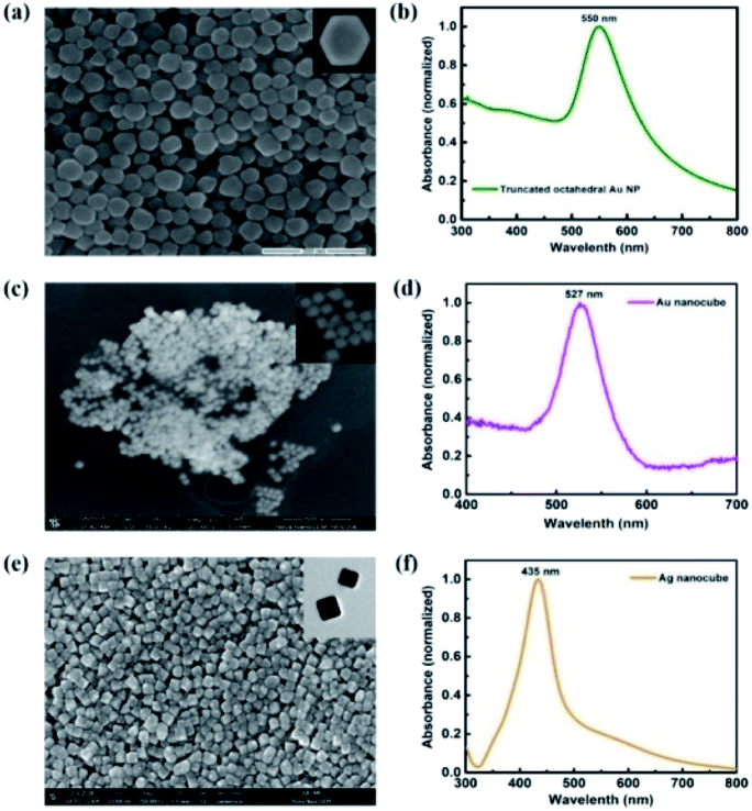 | ||
| Fig. 1 SEM image of (a) truncated octahedral Au NPs (c) Au NCs and (e) Ag NCs. UV-Vis absorption spectra of (b) truncated octahedral Au NPs (d) Au NCs and (f) Ag NCs. | ||
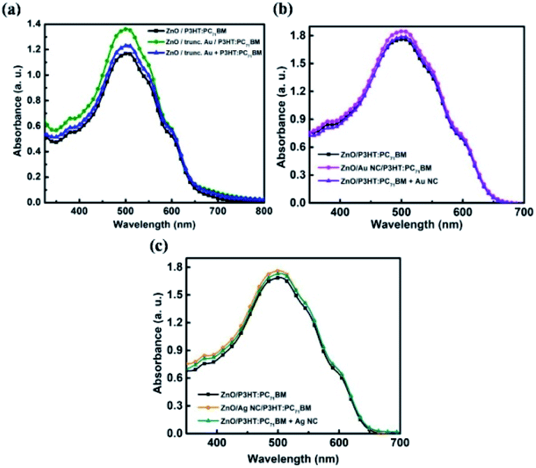 | ||
| Fig. 2 UV-vis absorption spectra of P3HT:PC71BM layer with and without (a) truncated octahedral Au NPs (b) Au NCs and (c) Ag NCs at different locations. | ||
The schematic of the device architectures used for inverted plasmonic BHJ OSCs is given in Fig. S1.† The current density–voltage (J–V) characteristics of P3HT:PC71BM based inverted BHJ OSCs, with and without metal NPs, are shown in Fig. 3(a), (c) and (e). Table 1 summarizes the performance parameters. The performance of POSCs by incorporating truncated octahedral Au NPs, Au NCs and Ag NCs in the active layer (device B, D and F) and also as an interfacial layer between ZnO/active layer (device C, E and G) are analysed. The reference P3HT:PC71BM device (device A) showed a PCE of 4.72%, open circuit voltage (Voc) of 624 mV, short circuit current density (Jsc) of 13.0 mA cm−2 and fill factor (FF) of 58.1%. The photovoltaic performance of POSCs is found to vary with the metal NPs shape, material and location in the POSC. Device B and C exhibit an enhancement in the PCE and Jsc with respect to the device A. However, the maximum enhancement is observed for device C. Compared to the device A, the PCE and Jsc of device C have improved by 20.3% and 30.0% respectively. In the case of Au NC based POSCs, the device E shows better performance than device D. Device E exhibits 11.4% enhancement in PCE and 27.7% in Jsc compared to device A. In the case of Ag NCs POSCs, device G shows better performance compared to that of device F. Device G exhibits 1.76% enhancement in PCE and 5.9% in Jsc compared to device F. Unlike Jsc, the Voc of the devices did not vary with the introduction of metal NPs. Hence the PCE improvement of POSCs is mainly due to the improved Jsc values. Increased Jsc on the addition of NPs confirms the improvement of light harvesting in the active layer for POSCs and is in synchronization with the observed enhancement of absorption in active layer using UV-Vis spectroscopy.
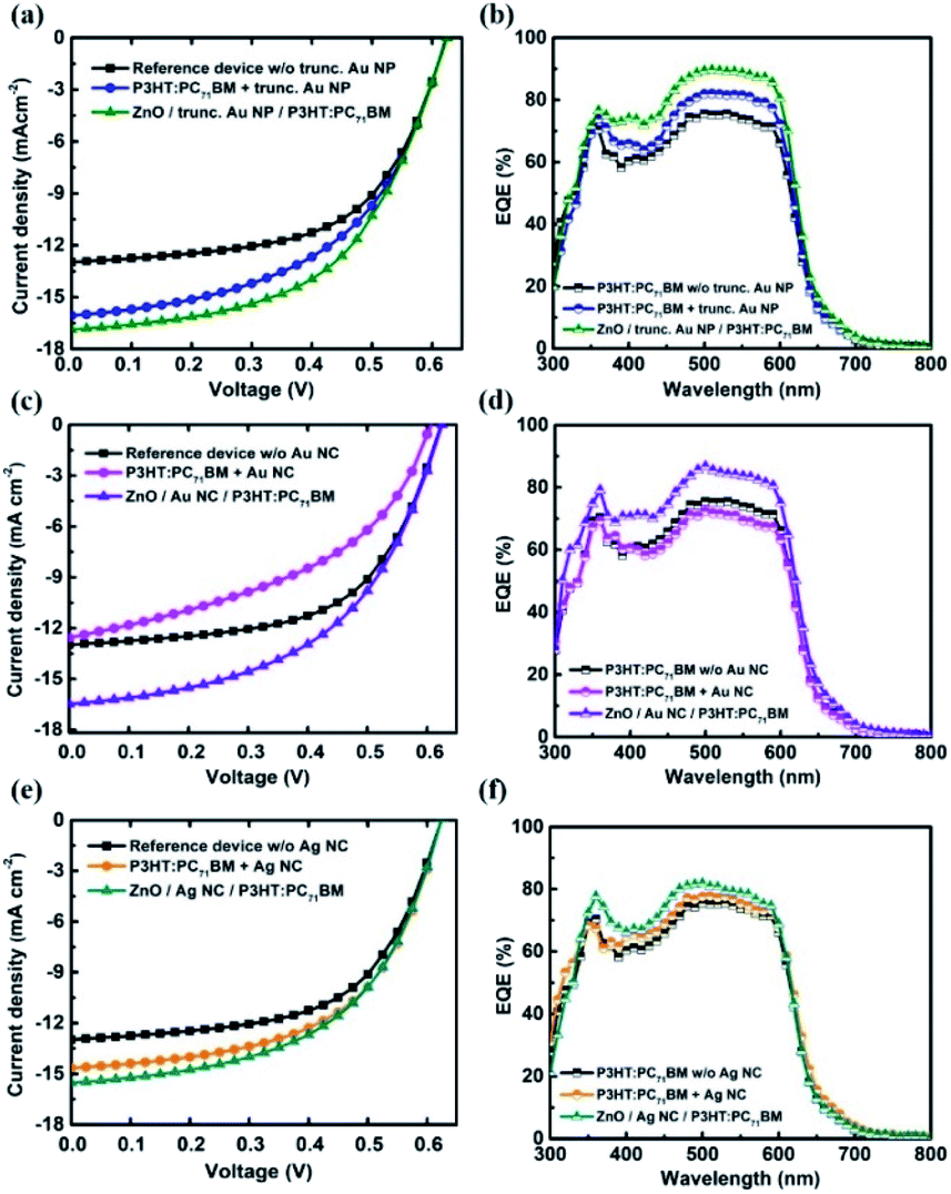 | ||
| Fig. 3 J–V characteristics of P3HT:PC71BM based devices without and with (a) truncated octahedral Au NPs (c) Au NCs and (e) Ag NCs incorporated at different positions of the OSC, and (b), (d) and (f) corresponds to the respective EQE with respect to wavelength. | ||
| Device | Position of metal NPs in the device | Voca (V) | Jsca (mA cm−2) | FFa (%) | PCEa (%) | Rs (Ω cm2) | Rsh (kΩc m2) | Jsc(EQE) (mA cm−2) |
|---|---|---|---|---|---|---|---|---|
| a Average value ± standard deviation (best value) of 5 devices fabricated and characterized under same conditions. | ||||||||
| A | Reference P3HT:PC71BM device | 0.623 ± 0.001 (0.624) | 12.80 ± 0.26 (13.01) | 57.95 ± 0.16 (58.12) | 4.62 ± 0.11 (4.72) | 104.49 | 5.55 | 10.82 |
| B | Trunc. octa. Au NP + P3HT:PC71BM | 0.622 ± 0.001 (0.623) | 16.00 ± 0.12 (16.12) | 50.93 ± 0.41 (51.38) | 5.07 ± 0.09 (5.16) | 85.68 | 3.85 | 11.77 |
| C | ZnO/Trunc. octa. Au NP/P3HT:PC71BM | 0.624 ± 0.001 (0.625) | 16.36 ± 0.47 (16.89) | 53.22 ± 0.50 (53.80) | 5.44 ± 0.21 (5.68) | 96.99 | 4.55 | 13.04 |
| D | Au NC + P3HT:PC71BM | 0.606 ± 0.001 (0.607) | 12.04 ± 0.60 (12.69) | 43.48 ± 0.89 (44.26) | 3.17 ± 0.23 (3.41) | 143.67 | 1.62 | 10.37 |
| E | ZnO/Au NC/P3HT:PC71BM | 0.623 ± 0.002 (0.625) | 16.23 ± 0.32 (16.60) | 50.26 ± 0.40 (50.69) | 5.09 ± 0.14 (5.26) | 93.37 | 3.57 | 12.51 |
| F | Ag NC + P3HT:PC71BM | 0.623 ± 0.001 (0.624) | 14.37 ± 0.31 (14.71) | 55.19 ± 0.42 (55.67) | 4.94 ± 0.15 (5.11) | 91.32 | 5.00 | 11.38 |
| G | ZnO/Ag NC/P3HT:PC71BM | 0.623 ± 0.001 (0.624) | 15.22 ± 0.32 (15.59) | 53.14 ± 0.26 (53.45) | 5.04 ± 0.14 (5.20) | 95.41 | 4.54 | 11.65 |
Comparing these results, it is observed that POSCs with metal NPs used as an interlayer between ZnO and the active layer exhibit the improved POSC performance. Among the devices C, E, and G, device C showed a maximum enhancement in PCE and Jsc. This can be due to the geometrical benefits of truncated octahedral Au NPs. Compared to cubes which have 8 vertices and 12 edges; truncated octahedral has 24 vertices and 36 edges. The sharp vertices of truncated octahedral Au NPs can give rise to a more concentrated field near particle and better LSPR coupling with the active material. Even though Ag NCs has better LSPR properties compared to that of Au NCs, POSCs with Ag NCs showed lower Jsc and PCE. Lower number of photons in the Ag NCs LSPR region compared to that of Au NCs LSPR region can be attributed to the low Jsc values observed for Ag NCs POSCs. Reproducibility of the device performance is verified by fabricating 20 devices in each structure and comparing the cell performance under same conditions. Fig. S2† shows the histogram of PCE vs. number of devices.
The best performing POSC (device C) showed a series resistance (Rs) of 85.68 Ω cm2 and shunt resistance (Rsh) of 3.85 kΩ cm2 compared to that of 104.49 Ω cm2 and 5.55 kΩ cm2 respectively for the device A. The low Rsh observed in the POSC can be due to agglomeration of NPs resulting in leakage current pathways. Low value of Rsh has reduced the FF of device C compared to the device A.
The improvement in Jsc can be further verified using the EQE measurement with POSCs and device A. Fig. 3(b), (d) and (f) shows the EQE spectra of POSCs and device A. All the POSCs showed enhanced EQE compared to that of device A and similar trend in enhancement as observed in J–V characteristic. The spectral envelope of the EQE followed UV-Vis absorption spectra of active layers. The spectral broadening observed in EQE is similar to that observed for absorption measurements and can be attributed to forward scattering and formation of aggregate of NPs. Among POSCs, device C showed better enhancement in EQE compared to all other POSCs. The EQE of the device A has a maximum value of 75.2% at ∼510 nm whereas the device C has maximum EQE value of 89.6% at ∼510 nm (an increase of 19.2%). The Jsc calculated from EQE spectra (Jsc (EQE)) is slightly less than the experimental values (Table 1). This can be due to the degradation of the device as the measurements are performed using unencapsulated device under ambient condition. The improved Jsc and EQE in the POSCs can be better understood by studying the exciton generation rate and the probability of exciton dissociation.
The improved Jsc and EQE are further evaluated using the maximum exciton generation rate (Gmax) and exciton dissociation probability (P(T,E)) studies. The photocurrent density (Jph) under AM 1.5G 1 Sun illumination from device A and POSCs are measured by applying a voltage sweep from 1 to −10 V.20 Fig. 4(a) shows the Jph dependence on effective voltage (Veff = Vo − Va; where Vo is the compensation voltage at Jph = 0 and Va is the applied voltage) for both device A and POSCs (best performing in each case – device C, device E and device G).20
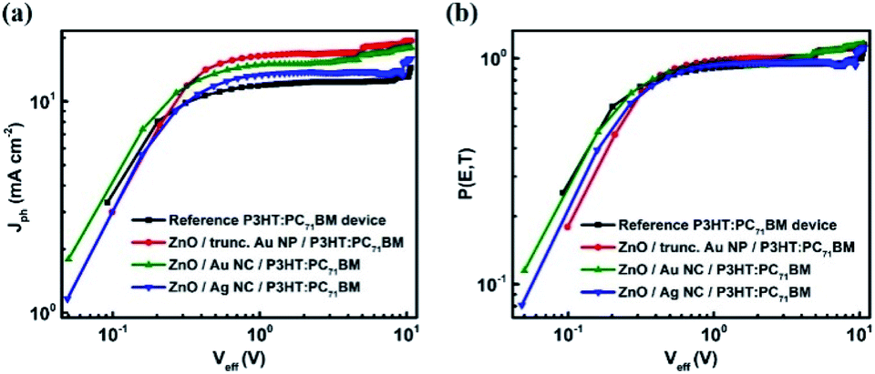 | ||
| Fig. 4 (a) Photocurrent (Jph) verses effective voltage (Veff) and (b) exciton dissociation probability [P(E,T)] vs. Veff for reference and plasmonic devices with P3HT:PC71BM as active layer. | ||
The Gmax values of the device A and the POSCs are tabulated in Table 2. Results show that Gmax has enhanced with the incorporation of NPs at the ZnO/active layer interface and maximum enhancement is observed for device C. Such an improvement can be attributed to the enhancement in the absorption of the active layer as observed in UV-Vis absorption spectra due to efficient LSPR coupling. Only a fraction of the photogenerated excitons dissociate into free carriers and is given by the P(E,T). The values of P(E,T) under the short-circuit condition (Va = 0) are obtained from the plot of P(E,T) vs. Veff (Fig. 4(b)). The maximum P(E,T) is obtained for device C. Gmax and P(E,T) values of devices B, D and F are evaluated from Fig. S3† and the values are tabulated in Table S1.†
| Device notation | Device structure | Gmax (m−3 s−1) | P(E,T) (%) |
|---|---|---|---|
| A | Reference P3HT:PC71BM device | 6.48 × 1027 | 87.01 |
| C | ZnO/Trunc. octa. Au NP/P3HT:PC71BM | 8.59 × 1027 | 95.62 |
| E | ZnO/Au NC/P3HT:PC71BM | 7.85 × 1027 | 92.82 |
| G | ZnO/Ag NC/P3HT:PC71BM | 7.17 × 1027 | 90.00 |
The results obtained from this study are consistent with the J–V characteristics and EQE measurements. The improvement in the performance of POSCs is further investigated using Raman spectroscopy to understand the coupling of LSPR with the active layer.
Raman spectroscopy is used to study the plasmonic effect and morphological changes (if any) in the P3HT:PC71BM system with the incorporation of metal NPs. SERS exhibits an enhanced Raman scattering for molecules lying in the vicinity of metal NPs.21 The enhancement can be due to: chemical enhancement and electromagnetic enhancement.22 The SERS effect of POSCs is studied with metal NPs as an interlayer (as these devices showed better performances compared to that of the blended ones). Since device C showed better performance among all the devices, truncated octahedral Au NPs case is considered first. Here, a thin layer of active material (20 nm) is coated on top of the NP layer. The Raman spectra of the reference sample (bare P3HT:PC71BM) and the plasmonic samples are recorded after exciting at 532 nm (Fig. 5 (a)).
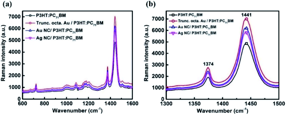 | ||
| Fig. 5 Raman spectra for P3HT:PC71BM without and with 5wt% Au NPs. The excitation wavelength is 532 nm. Raman spectra for P3HT:PC71BM without and with NPs for the wavenumber range of (a) 600 to 1600 cm−1(b) 1300 to 1500 cm−1. | ||
The Raman peaks observed at ∼1446 cm−1 and ∼1378 cm−1 for the P3HT:PC71BM layer can be attributed to the C![[double bond, length as m-dash]](https://www.rsc.org/images/entities/char_e001.gif) C in-plane stretching vibrations and the C–C skeletal stretching respectively. The band at ∼1206 cm−1 is due to the inter-ring C–C stretching whereas the peaks at ∼1085 cm−1 and ∼723 cm−1 correspond to the C–H bending mode with the C–C inter-ring stretching and the in-phase deformation vibration of C–S–C ring, respectively.23 An enhancement in the peak intensity of the plasmonic sample is observed with respect to the reference P3HT:PC71BM sample. However, the peak position of CC mode for both P3HT:PC71BM with and without the incorporation of truncated octahedral Au NP remains the same (∼1445 cm−1) (Fig. 5(b)). The full-width at half maxima (FWHM) of CC are almost constant (∼34 cm−1). The relative intensity ratio of C–C and CC modes (IC–C/ICC), for both reference and plasmonic film, are found to be 0.39. This rules out the possibility of any chemical enhancement with the addition of Au NPs as the morphology of P3HT:PC71BM film remains constant. Similar trend is observed in the case of Au and Ag NCs. Thus, the enhancement can be attributed to the electromagnetic field. The SERS enhancement for the CC mode at an excitation of 532 nm was calculated as the ratio of the area for P3HT:PC71BM peak in the presence of metal NPs to the area with metal NPs.24 The SERS enhancement for CC mode is calculated as 1.5, 1.3 and 1.2 for truncated octahedral Au NPs, Au NCs, and Ag NCs respectively. The device performance also follows the same sequence.
C in-plane stretching vibrations and the C–C skeletal stretching respectively. The band at ∼1206 cm−1 is due to the inter-ring C–C stretching whereas the peaks at ∼1085 cm−1 and ∼723 cm−1 correspond to the C–H bending mode with the C–C inter-ring stretching and the in-phase deformation vibration of C–S–C ring, respectively.23 An enhancement in the peak intensity of the plasmonic sample is observed with respect to the reference P3HT:PC71BM sample. However, the peak position of CC mode for both P3HT:PC71BM with and without the incorporation of truncated octahedral Au NP remains the same (∼1445 cm−1) (Fig. 5(b)). The full-width at half maxima (FWHM) of CC are almost constant (∼34 cm−1). The relative intensity ratio of C–C and CC modes (IC–C/ICC), for both reference and plasmonic film, are found to be 0.39. This rules out the possibility of any chemical enhancement with the addition of Au NPs as the morphology of P3HT:PC71BM film remains constant. Similar trend is observed in the case of Au and Ag NCs. Thus, the enhancement can be attributed to the electromagnetic field. The SERS enhancement for the CC mode at an excitation of 532 nm was calculated as the ratio of the area for P3HT:PC71BM peak in the presence of metal NPs to the area with metal NPs.24 The SERS enhancement for CC mode is calculated as 1.5, 1.3 and 1.2 for truncated octahedral Au NPs, Au NCs, and Ag NCs respectively. The device performance also follows the same sequence.
The LSPR effect on the improvement of active layer absorption can be further explored using steady-state PL measurements. The room temperature PL spectra of pristine P3HT without (glass/P3HT) and with metal NPs (glass/metal NPs/P3HT) were recorded. Fig. 6(a) and (b) present the PL spectra of P3HT in the absence and presence of truncated octahedral Au NPs. The samples are excited with two different wavelengths – 500 nm and 550 nm. In both the excitations, PL enhancement is observed for samples with Au NPs. For the excitation at 500 and 550 nm, the PL integrating intensity of the plasmonic layer was increased by 19% and 42% respectively, with respect to the reference P3HT layer. 550 nm excitation wavelength was chosen to match the plasmonic resonance frequency of the truncated octahedral Au NP. An enhancement at LSPR can be attributed to the effective coupling of LSPR of Au NPs with P3HT, which increases the photogenerated charge carriers in P3HT.25 The Au NC samples excited at 500 and 527 nm, exhibits enhancement of 16% and 39% respectively when compared to the reference P3HT layer (Fig. 6(c) and (d)). Similarly, for Ag NCs, the samples were excited at 500 nm and 435 nm where the latter corresponds to the LSPR peak wavelength of Ag NCs. Fig. 6(e) and (f) show that the PL enhancement is more for an excitation wavelength at 435 nm. As the sample is excited at 500 and 435 nm, the PL integrating intensity of the Ag NC/P3HT layer is enhanced by 18% and 26% with respect to the reference layer. Compared to Ag and Au NCs, truncated octahedral Au NPs have more PL integrating intensity enhancement at the LSPR wavelength excitation, which can be attributed to enhanced near-field effect due to higher number of antennas in the truncated octahedral Au NPs than in NCs. The results confirm the improved performance of device C.
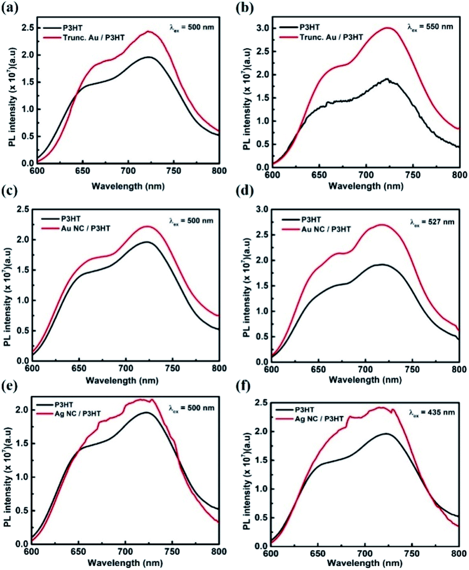 | ||
| Fig. 6 PL spectra of the P3HT layer with and without truncated octahedral Au NPs excited at (a) 500 nm, and (b) 550 nm. PL spectra of the P3HT layer with and without Au NCs excited at (c) 500 nm, and (d) 527 nm. PL spectra of the P3HT layer with and without Ag NCs excited at (e) 500 nm, and (f) 435 nm. | ||
Conclusions
Truncated octahedral Au NPs, Au NCs, and Ag NCs are synthesized and characterised using SEM and UV-Vis. These NPs are used to study the effect of NPs shape, material and incorporation location on P3HT:PC71BM based inverted BHJ OSC. POSCs with NPs incorporated as an interfacial layer between ZnO and active layer showed highest PCE and Jsc values for all kind of shapes and material. Near-field enhancement as well as enhanced forward scattering cross section is attributed for POSC performance improvement. Among the NPs with two shapes, POSCs with truncated octahedral Au NPs exceeded the photovoltaic performance compared to those of POSCs with Au and Ag NCs. Large number of antennas in truncated octahedral Au NPs compared to NC is reasoned to be the cause for this improvement. Even though Ag has better LSPR properties compared to Au, the POSCs with Ag NCs showed lower Jsc value and is due to reduced number of photons at the blue shifted LSPR wavelength of Ag NCs. The improvement in Jsc values of POSCs is confirmed by enhancement in absorption, EQE, exciton generation and exciton dissociation probability measurements and is due to improved LSPR coupling of the NPs with the active layer. The SERS and PL studies confirm the absorption enhancement in the active layer by NP LSPR coupling and further confirm the enhancement in the photovoltaic performance of POSCs.Conflicts of interest
There are no conflicts to declare.Acknowledgements
The authors acknowledges financial support from the Solar Energy Research Initiative (Department of Science and Technology, Government of India) (Grant reference number: DST/TMD/SERI/S15(G)), Ministry of Human Resource Development (Government of India), and Indian Institute of Science Education and Research Thiruvananthapuram (IISER TVM), Kerala, India.References
- K. Roy, C. Vinod and C. S. Gopinath, J. Phys. Chem. C, 2013, 117, 4717–4726 CrossRef CAS.
- K. Roy and C. S. Gopinath, Anal. Chem., 2014, 86, 3683–3687 CrossRef CAS PubMed.
- D. B. Mitzi, K. Chondroudis and C. R. Kagan, IBM J. Res. Dev., 2001, 45, 29–45 CAS.
- P. P. Boix, S. Agarwala, T. M. Koh, N. Mathews and S. G. Mhaisalkar, J. Phys. Chem. Lett., 2015, 6, 898–907 CrossRef CAS PubMed.
- B. Kippelen and J.-L. Brédas, Energy Environ. Sci., 2009, 2, 251–261 RSC.
- Y. Cui, Y. Wang, J. Bergqvist, H. Yao, Y. Xu, B. Gao, C. Yang, S. Zhang, O. Inganäs and F. Gao, Nat. Energy, 2019, 4, 768–775 CrossRef CAS.
- X. Guo, N. Zhou, S. J. Lou, J. Smith, D. B. Tice, J. W. Hennek, R. P. Ortiz, J. T. L. Navarrete, S. Li and J. Strzalka, Nat. Photon., 2013, 7, 825 CrossRef CAS.
- A. C. Mayer, S. R. Scully, B. E. Hardin, M. W. Rowell and M. D. McGehee, Mater. Today, 2007, 10, 28–33 CrossRef CAS.
- K. Tvingstedt, Z. Tang and O. Inganäs, Appl. Phys. Lett., 2012, 101, 163902 CrossRef.
- B. V. Andersson, U. Wuerfel and O. Inganäs, Sol. Energy, 2011, 85, 1257–1263 CrossRef.
- L. Feng, M. Niu, Z. Wen and X. Hao, Polymers, 2018, 10, 123 CrossRef PubMed.
- S. K. Cushing, A. D. Bristow and N. Wu, Phys. Chem. Chem. Phys., 2015, 17, 30013–30022 RSC.
- W. R. Erwin, R. C. MacKenzie and R. Bardhan, J. Phys. Chem. C, 2018, 122, 7859–7866 CrossRef CAS.
- A. V. Gaikwad, P. Verschuren, S. Kinge, G. Rothenberg and E. Eiser, Phys. Chem. Chem. Phys., 2008, 10, 951–956 RSC.
- H. Chen, X. Kou, Z. Yang, W. Ni and J. Wang, Langmuir, 2008, 24, 5233–5237 CrossRef CAS PubMed.
- S. E. Skrabalak, L. Au, X. Li and Y. Xia, Nat. Protoc., 2007, 2, 2182 CrossRef CAS PubMed.
- P. Aneesh, C. R. Kumar, P. R. Varma, K. Vivek and M. A. Namboothiry, Org. Photonics Photovoltaics, 2015, 3, 64–70 Search PubMed.
- S. D. Stranks, G. E. Eperon, G. Grancini, C. Menelaou, M. J. Alcocer, T. Leijtens, L. M. Herz, A. Petrozza and H. J. Snaith, Science, 2013, 342, 341–344 CrossRef CAS PubMed.
- M. Dante, J. Peet and T.-Q. Nguyen, J. Phys. Chem. C, 2008, 112, 7241–7249 CrossRef CAS.
- V. Mihailetchi, L. Koster, J. Hummelen and P. Blom, Phys. Rev. Lett., 2004, 93, 216601 CrossRef CAS PubMed.
- C. Kagan, D. Mitzi and C. Dimitrakopoulos, Science, 1999, 286, 945–947 CrossRef CAS PubMed.
- M. J. Seo, G. W. Kim, P. V. Tsalu, S. W. Moon and J. W. Ha, Nanoscale Horiz., 2020, 5, 345–349 RSC.
- S. Falke, P. Eravuchira, A. Materny and C. Lienau, J. Raman Spectrosc., 2011, 42, 1897–1900 CrossRef CAS.
- M. Stavytska-Barba, M. Salvador, A. Kulkarni, D. S. Ginger and A. M. Kelley, J. Phys. Chem. C, 2011, 115, 20788–20794 CrossRef CAS.
- J.-L. Wu, F.-C. Chen, Y.-S. Hsiao, F.-C. Chien, P. Chen, C.-H. Kuo, M. H. Huang and C.-S. Hsu, ACS Nano, 2011, 5, 959–967 CrossRef CAS PubMed.
Footnote |
| † Electronic supplementary information (ESI) available. See DOI: 10.1039/d0ra04076b |
| This journal is © The Royal Society of Chemistry 2020 |