
 Open Access Article
 This Open Access Article is licensed under a
 Creative Commons Attribution 3.0 Unported Licence
Retracted Article: Wavelength modulation of ZnO nanowire based organic light-emitting diodes with ultraviolet electroluminescence
Runze Chena,
Chuan Liub,
Kyeiwaa Asare-Yeboahc,
Ziyang Zhangd,
Zhengran He *e and
Yun Liu*f
*e and
Yun Liu*f
aLeicester International Institute, Dalian University of Technology, Panjin City, 124221, China
bState Key Laboratory of Structural Analysis for Industrial Equipment, Dalian University of Technology, Dalian 116024, China
cDepartment of Electrical and Computer Engineering, Penn State Behrend, Erie, PA 16563, USA
dDepartment of Electrical Engineering, Columbia University, New York City, NY 10027, USA
eDepartment of Electrical and Computer Engineering, The University of Alabama, Tuscaloosa, AL 35487, USA. E-mail: zhe3@crimson.ua.edu
fDepartment of Physics, Dalian University of Technology, Dalian 116024, China. E-mail: liuyun89@dlut.edu.cn
First published on 22nd June 2020
Abstract
Although organic light emitting diodes (OLEDs) can find important applications in display-related fields, it still remains a challenge to fabricate high-efficiency ultraviolet (UV) OLEDs with tunable wavelength. In this work, we demonstrate a facile method to adjust the electroluminescence (EL) peak from an inverted UV-OLED device that has zinc oxide nanowires (ZnO NWs) as an electron injection layer. The organic–inorganic interface between ZnO NWs and the 3-(4-biphenyl)-4-phenyl-5-tert-butylphenyl-1,2,4-triazole (TAZ) emission layer employed in this work allows a reduction of the diffusion length of excitons, which further results in a hampered relaxation process of higher energy states as well as a blue shift of the EL spectrum. As a result, the emission peaks of the UV-OLED can be easily adjusted from 383 nm to 374 nm by tuning both the length of the ZnO NWs and the thickness of the TAZ emission layer. Our work reveals an important correlation between emission peaks and exciton diffusion, and presents a novel approach to fabricate high-performance UV-OLEDs with the capability of facilely modifying the emission wavelength.
1. Introduction
Recently, organic light emitting diodes (OLEDs) have been extensively studied for their various advantages such as solution-processability, cost-effectiveness, and room temperature processing.1–6 In particular, due to their capability of emitting high-energy ultraviolet (UV) light, high-efficiency UV-OLEDs demonstrate great significance for IT storage, photocuring, aerospace, medical and military applications.7,8 In addition, UV-OLEDs can be potentially implemented in RGB screens. By tuning the material choice and device configuration, different emission peaks from the UV-OLEDs can be facilely realized.9 Nanowires (NWs) as active layers of UV-OLEDs have attracted considerable attention due to their unique merits as compared to the thin film based devices.10–13 While thin films may exhibit an abundance of grain boundaries and joint defects,14–18 where non-radiative recombinations can occur, NWs effectively circumvent this issue and exhibit enhanced emission efficiency.19 Besides, because of the less contact areas between the n-type and p-type semiconductor materials, epitaxial heterojunctions exhibit fewer defect densities and interfacial strains.20 Due to these properties, integrated NWs can be an ideal candidate for the fabrication of short-wavelength OLEDs.Zinc oxide (ZnO) NWs have been well known for their properties of lower temperature sensitivity and enhanced confinement of charge carriers in one dimensional nanostructures,21–24 which enables the material to be implemented in optoelectronics and energy harvesting.25–28 A plethora of efforts have been dedicated to the reduction of the electroluminescence (EL) wavelength from ZnO NWs based OLEDs. For example, Zhang et al. reported the deposition of ZnO NWs on a GaN-on-sapphire substrate by using physical vapor deposition, and observed a blue shift from 440 nm to 400 in the EL spectrum by increasing the forward voltage.29 Dong et al. developed the hydrothermal growth of ZnO NWs on a GaN layer for UV-LED fabrication, which demonstrated an intensive emission at 390 nm and also strong waveguiding properties with reduced diameter in ZnO NWs.30 Similarly, Tang and coworkers reported that ZnO NWs were grown as a continuation on vertically-aligned p-type AlGaN NWs which had different diameters from 100 nm to 500 nm. Each nanowire formed a p–n heterojunction structure, yielding a single peak at 394 nm.31 More recently, Gao et al. demonstrated the fabrication of ZnO NWs based Schottky LEDs with an excitonic luminescence peak at 380 nm under a high forward bias current.32 Despite these efforts, there have been no studies regarding UV-OLEDs with tunable emission peak wavelength below 380 nm.
In this work, we report the fabrication of an inverted UV-OLED device with vertically-aligned, self-assembled ZnO NWs employed as an electron transport layer. The metallic nature of ZnO NWs allows the successful tuning of the exciton lifetime and relaxation time. The effect of the different nanowire length on the EL spectrum and peak locations was investigated. The electrical performance of the UV-OLED was further optimized by tuning the thickness of the emission layer. As a result, the ZnO NWs based UV-OLED demonstrates excellent tunability of wavelength from 383 nm to 374 nm. The blue shift of 9 nm in the emission peaks was achieved by means of engineering device structures as opposed to tuning material properties as reported in previous studies. Our important findings open up a new pathway for advancing display technology by using single ultraviolet light as an excitation source.
2. Experimental section
The fabrication of UV-OLEDs was based on the indium tin oxide (ITO) coated glass substrates, which served as the cathode. The detailed fabrication procedure of UV-OLEDs is as follows. The ITO substrates were first cleaned in liquid detergent, deionized water, acetone, and isopropanol, respectively, each for 30 minutes in an ultrasonic bath. Then the substrates were treated with oxygen plasma for 10 minutes to remove the organic residues. A more polarized ITO surface allows for better adhesion of the ZnO precursor. A 10 nm ZnO seed layer was sputtered onto the pre-cleaned ITO glass followed by growing ZnO NWs using a hydrothermal method.33–35 The polyethylenimine (PEI) material was spin-coated from a 0.4 wt% 2-methoxyethanol solution (5000 rpm, 50 seconds).36 Then, the films were thermally annealed in an ambient environment for 10 minutes at a temperature of 100 °C. After thermal annealing, 3-(4-biphenyl)-4-phenyl-5-tert-butylphenyl-1,2,4-triazole (TAZ) as an emission layer and 2,9-dimethyl-4,7-dipheny-l-1,10-phenanthroline (CBP) as a hole transport layer were thermally evaporated on PEI layer, respectively. Afterwards, molybdenum oxide (MoO3) and aluminum (Al) materials were sequentially deposited via thermal evaporation at a pressure of 4 × 10⁻⁴ Pa. The evaporation rate is 0.2–0.4 Å s−1 for MoO3, and 5 Å s−1 for Al. The as-fabricated UV-OLED device exhibits an inverted structure of ITO (100 nm)/ZnO NWs/PEI (4 nm)/TAZ (15 nm)/CBP (20 nm)/MoO3 (5 nm)/Al (100 nm), as shown in the schematic of Fig. 2(a). The thickness of the ZnO nanowire layer varies depending on different nanowire length (300 nm, 600 nm, 900 nm and 1200 nm).The current density–voltage (J–V) characteristics of the UV-OLED were measured by using a Keithley 2450 source unit. Simultaneously the EL spectrum was measured by using a QE65 Pro Spectra Scan from Ocean Optics. External quantum efficiency was calculated based on the electrical and optical measurement results.
3. Results and discussion
The molecular structures of the materials including CBP, PEI and TAZ were shown in Fig. 1(a). ZnO NWs were employed as the electron transport layer in this work due to their high electron mobility and unique photonic, semiconducting, and piezoelectric properties.25 ZnO NWs have a wide band gap of ∼3.30 eV and a large exciton binding energy of ∼60 meV. Since UV-emitting material requires a large bandgap due to the high photon energy and corresponding energy loss prior to de-excitation, ZnO NWs are considered as an ideal candidate for fabricating high-efficiency photodetectors and nanosized heterojunction LEDs.37,38 In addition, owing to its metallic nature and the exciton dissociation effect at the inorganic–organic interface,39 ZnO NWs serve as an excellent active layer choice for regulating the exciton relaxation. The cross-section scanning electron microscopy (SEM) image of self-assembled ZnO NWs was presented in Fig. 1(b), which showed that the NWs were uniformly aligned in the vertical direction. Fig. 1(c) is a digital image of an as-fabricated UV-OLED device with ZnO NWs as an electron transport layer, which shows its capability to examine the anti-counterfeiting mark on a Chinese dollar bill.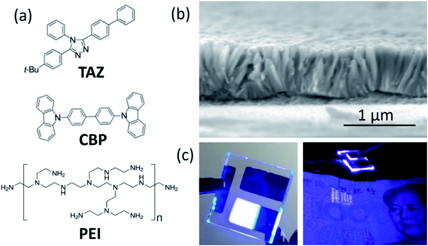 | ||
| Fig. 1 (a) The molecular structures of organic materials including TAZ, CBP and PEI. (b) A cross-sectional SEM image of the vertically-aligned, self-assembled ZnO NWs. (c) A digital picture showing the as-fabricated UV-OLED device, which is used to examine the anti-counterfeiting mark on a Chinese dollar bill. | ||
3.1 Effect of ZnO NWs length on the EL spectra
Electroluminescence is as a result of radiative recombination of holes and electrons within the material. The excited electrons release energy as photons, which gives rise to the emission of light. In order to understand how different length of the ZnO NWs impacted the electrical performance of the UV-OLED, we have fabricated four different types of UV-OLEDs with 300 nm, 600 nm, 900 nm and 1200 nm length of ZnO NWs. The resultant EL spectra of the UV-OLED were presented in Fig. 2(b), which shows a dependence of peak location and intensity on the length of ZnO NWs. The peak locations were extracted and more clearly plotted in Fig. 2(c) as a function of the nanowire length. It can be seen that with the ZnO nanowire length of 300 nm, 600 nm, 900 nm and 1200 nm, the peak positions were observed to be at 378.5 nm, 378 nm, 376 nm and 374 nm, respectively, indicating a blue shift of the EL spectra as the ZnO nanowire length increases. Such a blue shift can be attributed to the larger contact area between the ZnO NWs and the TAZ layer, resulting in enhanced effect on electron hopping from the highest excitation state to the lowest excitation state, as well as shorter lifetime of excitons. The external quantum efficiency (EQE) was calculated to be 1.12%, 0.61%, 0.43% and 0.29% with the ZnO nanowire length of 300 nm, 600 nm, 900 nm and 1200 nm, respectively, as shown in the plot of Fig. 2(d).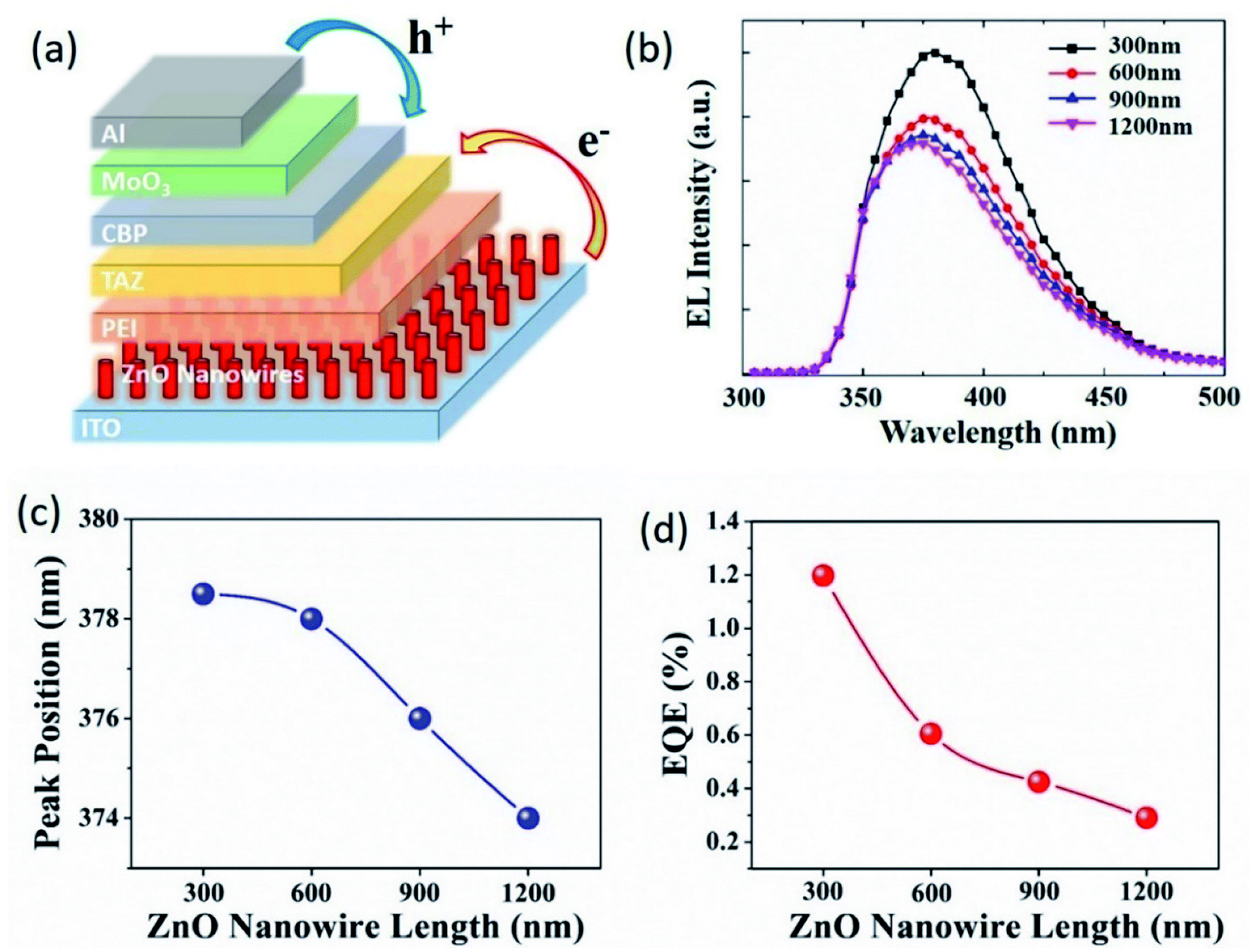 | ||
| Fig. 2 (a) Schematic of device configuration of ZnO NWs based UV-OLED. The device comprises an inverted structure of ITO (100 nm)/ZnO NWs/PEI (4 nm)/TAZ (15 nm)/CBP (20 nm)/MoO3 (5 nm)/Al (100 nm). The thickness of the ZnO nanowire layer varies depending on different nanowire length. (b) EL spectra of the UV-OLED as a function of the different length of the ZnO NWs, including 300 nm, 600 nm, 900 nm and 1200 nm. (c) A plot of the peak position corresponding to each different ZnO nanowire length, clearly indicating a blue shift as the nanowire length increases. (d) EQE as a function of different ZnO nanowire length. | ||
3.2 Relaxation model of exciton
The electric potential diagram of the UV-OLED device is shown in schematic of Fig. 3(a). Since ZnO NWs have a much lower lowest unoccupied molecular orbital (LUMO) (≈−4.4 eV) than that of TAZ (≈−2.8 eV), a thin layer of PEI was sandwiched between ZnO NWs and TAZ. The PEI interface layer effectively induces the formation of interfacial dipoles and reduces the LUMO difference between ZnO and TAZ, favorable for electron injection.40 An inorganic p-type metal oxide layer MoO3, which has a high work function, was employed as the hole injection layer, in order to lower the injection barrier between the organic film and the metal electrode.41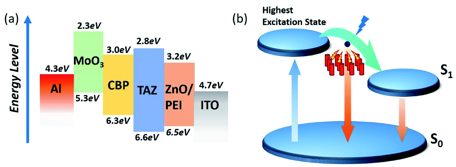 | ||
| Fig. 3 (a) Schematic showing the typical potential diagram of the inverted UV-OLED. Since ZnO NWs have a much lower LUMO (≈−4.4 eV) than that of TAZ (≈−2.8 eV), a thin layer of PEI was sandwiched between ZnO and TAZ in order to facilitate electron injection. (b) Schematic depicting the principle of exciton relaxation time modified by ZnO NWs. | ||
The schematic of Fig. 3(b) depicts the principle of the exciton relaxation time, which plays an important role in the operation of various solid-state devices including fluorescent OLED,42 thermally activated delayed fluorescent (TADF) OLED,43 phosphorescent OLED,44 and organic photovoltaic cells.45 Electrons first hop to the highest excitation state, relax to the lowest excitation state, and then hop from LUMO to HOMO of TAZ to combine with holes. As the incorporation of ZnO NWs interrupts the relaxation process between the highest excitation state and the lowest excitation state, electrons directly hop down to combine with holes, leading to a wider bandgap and shorter emission wavelength. The more contact area between TAZ and ZnO NWs, the more pronounced this effect is. Among a few physical phenomena that have been reported to control the performance of optoelectronic devices, exciton diffusion impacts the energy state of excitons and thereby the location of the emission peaks in OLED.46 Different factors can influence the exciton diffusion and lifetime including different temperature, electrode configuration and quench agent, which would also result in luminescence position deviation.
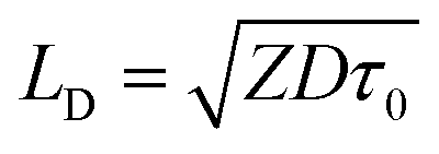
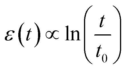
Because of the metallic nature of the ZnO NWs, the excitons in the TAZ emission layer can be resolved based on the exciton diffusion at the ZnO nanowire interface. Long-range non-radiative energy transfer of excitons can occur between dipole (organic molecule in excited states) and ZnO NWs, which can shorten the exciton lifetime.39,47 The average moving distance of excitons within their lifetime, i.e. the distance between the starting point and final arrival point, can be determined by the diffusion length LD:48
 | (1) |
From another perspective, the exciton diffusion can be described as a continuous process of non-radiative energy transfer among multiple molecules. Singlet excitons, which include those from the TAZ emission layer, primarily transfer among molecules in the fashion of Förster energy transfer. Based on the various external factors that affect the molecular energy level, the density of excitonic states (DOS) is expressed by a Gaussian distribution described in the following eqn (2):49
ρ(ε) = (2πσ2)−1/2![[thin space (1/6-em)]](https://www.rsc.org/images/entities/char_2009.gif) exp{−ε2/(2σ2)} exp{−ε2/(2σ2)}
| (2) |
 | (3) |
As shown in the schematic of Fig. 4(a), excitons from a high-energy state tend to hop towards a low-energy state but cease to spread as the energy reaches the most populated states. When compared to those with short diffusion lengths, excitons with longer diffusion lengths (accordingly lower energy) have a higher tendency to have non-radiative energy transfer with ZnO NWs, which as a result reduces the lifetime random walk excitons. This process facilitates the most populated states to migrate to a higher energy state.51 Fig. 4(b) shows a schematic diagram of the zones of exciton formation. Fig. 4(c) depicts the relaxation process of excitons. Based on the energy model shown in the diagram, excitons of lower energy result in longer radiation wavelength. The enhanced organic–inorganic interface as a result of employing the ZnO NWs as an electron transport layer effectively reduced the diffusion length of excitons, which further results in a hampered relaxation process of higher energy states.
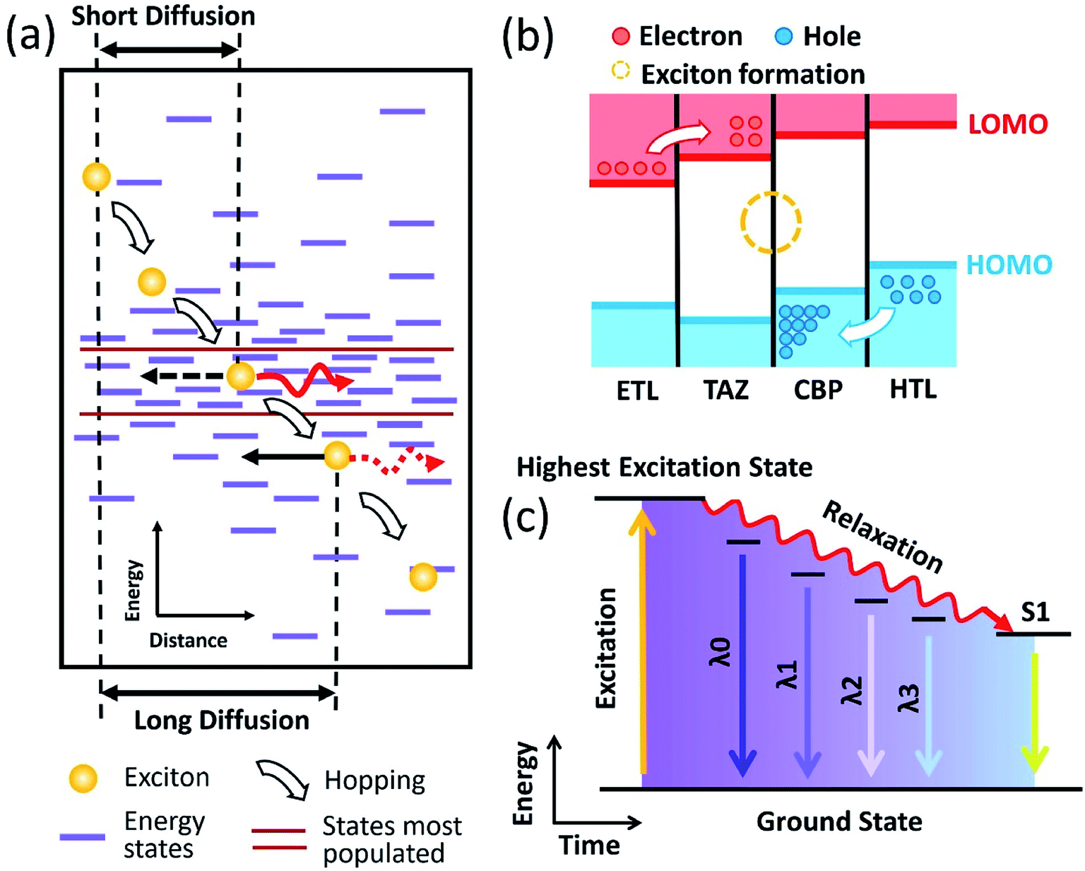 | ||
| Fig. 4 (a) Schematic illustration of the different exciton diffusion process in the UV-OLED device, which depicts both a short diffusion process and a long diffusion process. The energy distribution of excitonic states can be expressed by the Gaussian density of states. (b) Schematic illustrating the exciton formation. (c) Schematic depicting the relaxation process of excitons. Based on the energy model, lower energy results in longer radiation wavelength. | ||
3.3 Effect of the emission layer thickness on the EL spectra
In order to further enhance the hole injection and optimize the electrical performance of the UV-OLED, we fabricated a series of ZnO NWs based UV-OLED devices by varying the TAZ layer thickness. The device configuration comprises a structure of ITO (100 nm)/ZnO NWs/PEI (4 nm)/TAZ (x nm)/CBP (20 nm)/MoO3 (5 nm)/Al (100 nm), with x = 15, x = 25, x = 35 and x = 45. The length of the ZnO NWs was fixed at 600 nm. The EL spectra of the UV-OLED were plotted as a function of different thickness of the TAZ layer, as presented in Fig. 5(a). It can be obviously seen that as the thickness of TAZ emission layer increases, the luminescence spectrum shows a blue shift. The peaks at 383 nm, 381.8 nm, 381 nm, and 379.1 nm were identified with the TAZ emission layer thickness of 15 nm, 25 nm, 35 nm and 45 nm, respectively, as shown in Fig. 5(b). Nevertheless, continuous increase in the TAZ layer thickness may not result in further blue shifting of the EL spectra. This can be attributed to the hole accumulation at the interface between the TAZ and CBP layer because of the electron transport behaviors of the TAZ and quenching of the excitons,52 as depicted in Fig. 4(b).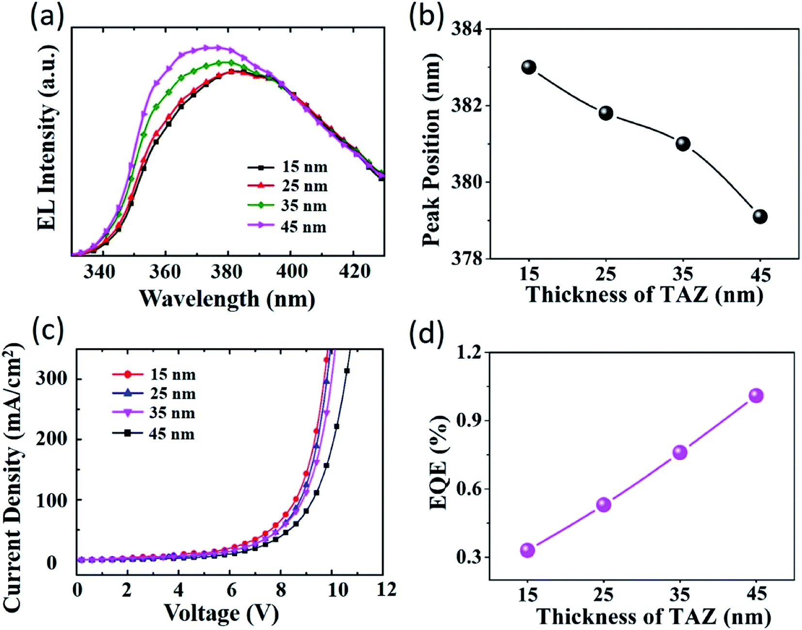 | ||
| Fig. 5 Influence of the different thickness of the emission layer TAZ on the electrical properties of UV-OLED. (a) EL spectra of UV-OLED as a function of different emitter layer thickness, including 15 nm, 25 nm, 35 nm and 45 nm. (b) Peak positions as a function of different TAZ layer thickness. In particular, the peaks were observed to be at 383 nm, 381.8 nm, 381 nm and 379.1 nm with the corresponding TAZ thickness of 15 nm, 25 nm, 35 nm and 45 nm, respectively. (c) J–V characteristics of the inverted UV-OLED with different TAZ thickness. (d) A plot showing the calculated EQE results as a function of different TAZ layer thickness. EQE of 0.33%, 0.53%, 0.76% and 1.01% were obtained with the 15 nm, 25 nm, 35 nm and 45 nm thickness of TAZ layer, respectively. | ||
The J–V characteristics of the UV-OLED device with different TAZ emission layer thickness were presented in Fig. 5(c). Based on the same current density shown in the J–V characteristics, reduction in the thickness of TAZ from 45 nm to 15 nm results in reduced driving voltage. Reduced TAZ thickness can have a lower resistance, which would increase the occurrence of unbound holes and electrons and thereby induce less combinations. According to the experimental data, as the TAZ thickness increases by 30 nm, the operating voltage increases by approximately 0.5 V under the current density of 300 mA cm−2. Therefore, the average electric field of the TAZ film calculated at this particular current density was 1.67 × 10⁷ V m−1. The EQE of UV-OLEDs were calculated to be 0.33%, 0.53%, 0.76% and 1.01% with the 15 nm, 25 nm, 35 nm and 45 nm thickness of TAZ layer, respectively, as shown in the plot of Fig. 5(d). Higher external quantum efficiency can be attributed to enhanced hole injection ability and strong binding of the charge carriers. When electrons are injected into the TAZ layer, subsequently they can be more easily transferred to the TAZ/CBP interface, due to their higher mobility than holes. However, for holes transported to the TAZ/CBP interface, only a portion of them can be injected across the interface barrier into the TAZ layer at a slow transfer rate, which gives rise to the shifting of the exciton formation region towards the TAZ/CBP interface. In contrast, holes blocked by the TAZ/CBP interface can quench the excitons during diffusion. Multiple hole transport layers (HTLs) can enhance the hole transport capability, resulting in better combination of holes and electrons in the emitting layer. As a result of the hole-blocking process, the EL peaks of the inverted UV-OLED device can be facilely tuned by adjusting the TAZ layer thickness. As the emission layer thickness increases, the hole-blocking effect can become more predominant. A thicker TAZ emission layer can result in reduced lifetime of the random walkers, and thereby limit the shift of the most popular states towards a higher level, which may otherwise cause the blue shift of the EL spectrum.
4. Conclusions
In summary, we have successfully demonstrated the fabrication of an inverted UV-OLED device by employing wide band gap ZnO NWs as an electronic transport layer. By tuning the length of the ZnO NWs, a luminous peak at 374 nm was observed which was lower than the values reported in most previous literatures. The blue shift of EL peaks with increasing length of the ZnO NWs is attributed to their corresponding larger contact area with TAZ, which leads to stronger effect on electron hopping from the highest excitation state to the lowest excitation state, as well as shorter lifetime of excitons. A dynamic model of excitons was proposed to understand the exciton diffusion and relaxation of the inverted UV-OLED. This model was further employed to study how different thickness of the TAZ layer impacts the peak intensities and locations of the EL spectrum. A blue shift in the EL spectra was observed as the TAZ layer thickness increases from 15 nm to 45 nm. Our work can be facilely applied to enhance the efficiency, tune the emission wavelength and optimize the electrical performance of other types of OLEDs in general.Conflicts of interest
The authors declare no conflicts of interests.References
- S.-K. Kwon, J.-H. Baek, H.-C. Choi, S. K. Kim, R. Lampande, R. Pode and J. H. Kwon, RSC Adv., 2019, 9(72), 42561–42568 RSC.
- W. A. D. M. Jayathilaka, A. Chinnappan, J. N. Tey, J. Wei and S. Ramakrishna, J. Mater. Chem. C, 2019, 7(19), 5553–5572 RSC.
- Q. Li, S. Bi, K. Asare-Yeboah, J. Na, Y. Liu, C. Jiang and J. Song, ACS Nano, 2019, 13(7), 8432 Search PubMed.
- G. Chen, Y. Weng, F. Sun, X. Zhou, C. Wu, Q. Yan, T. Guo and Y. Zhang, RSC Adv., 2019, 9(36), 20884–20891 RSC.
- S. Bi, Q. Li, Z. He, Q. Guo, K. Asare-Yeboah, Y. Liu and C. Jiang, Nano Energy, 2019, 66, 104101 CrossRef CAS.
- S. Bi, Q. Li, K. Asare-Yeboah, J. Na, Y. Sun and C. Jiang, J. Phys. Chem. Lett., 2020, 11(10), 3947–3954 CrossRef CAS PubMed.
- T. Fujii, Y. Gao, R. Sharma, E. L. Hu, S. P. DenBaars and S. Nakamura, Appl. Phys. Lett., 2004, 84(6), 855–857 CrossRef CAS.
- A. Mikami, Y. Mizuno and S. Takeda, High efficiency ultraviolet light emitting organic devices and its application to white light source, SID Int. - Symp. Dig. Tech. Pap., 2008, 1–3 Search PubMed.
- G. Luka, D. Volyniuk, A. Tomkeviciene, J. Simokaitiene, J. V. Grazulevicius, P. Stakhira, V. Cherpak, P. Sybilski, B. S. Witkowski, M. Godlewski, E. Guziewicz, Z. Hotra and O. Hotra, Oxide Materials for Electronic Engineering - Fabrication, Properties and Applications, 2013, vol. 200, pp. 45–49 Search PubMed.
- X. Qu and J. Gu, RSC Adv., 2020, 10(3), 1243–1248 RSC.
- G.-Q. Wei, X.-D. Wang and L.-S. Liao, Adv. Funct. Mater., 2019, 29(32), 1902981 CrossRef.
- C. Isenberg, E. B. Käkel, T. P. I. Saragi, P. Thoma, B. Weber and A. Lorenz, RSC Adv., 2019, 9(4), 1807–1813 RSC.
- X. Zhao, H. Xu, Z. Wang, Y. Lin and Y. Liu, InfoMat, 2019, 1(2), 183–210 Search PubMed.
- Z. He, J. Chen and D. Li, Soft Matter, 2019, 15(29), 5790–5803 RSC.
- Z. He, Z. Zhang, K. Asare-Yeboah and S. Bi, J. Mater. Sci.: Mater. Electron., 2019, 30, 14335–14343 CrossRef CAS.
- Z. He, Z. Zhang, S. Bi, J. Chen and D. Li, Sci. Rep., 2020, 10(1), 4344 CrossRef PubMed.
- Z. He, Z. Zhang, S. Bi, K. Asare-Yeboah and J. Chen, J. Polym. Res., 2020, 27(3), 75 CrossRef CAS.
- Z. He, J. Chen and D. Li, J. Vac. Sci. Technol., A, 2019, 37(4), 040801 CrossRef.
- O. Lupan, T. Pauporte and B. Viana, Adv. Mater., 2010, 22(30), 3298–3302 CrossRef CAS PubMed.
- S. Bi, Q. Li, Y. Yan, K. Asare-Yeboah, T. Ma, C. Tang, Z. Ouyang, Z. He, Y. Liu and C. Jiang, Phys. Chem. Chem. Phys., 2019, 21(5), 2540–2546 RSC.
- Y.-J. Liao, C.-W. Cheng, B.-H. Wu, C.-Y. Wang, C.-Y. Chen, S. Gwo and L.-J. Chen, RSC Adv., 2019, 9(24), 13600–13607 RSC.
- D. Kim, S. H. R. Shin, Y. Kim, K. Crossley, Y. Kim, H. Han and J. Yoo, RSC Adv., 2020, 10(23), 13655–13661 RSC.
- M. Pusty and P. M. Shirage, RSC Adv., 2020, 10(17), 10097–10112 RSC.
- L. Chen, Y. Cui, Z. Xiong, M. Zhou and Y. Gao, RSC Adv., 2019, 9(38), 21831–21843 RSC.
- S. Xu, C. Xu, Y. Liu, Y. F. Hu, R. S. Yang, Q. Yang, J. H. Ryou, H. J. Kim, Z. Lochner, S. Choi, R. Dupuis and Z. L. Wang, Adv. Mater., 2010, 22(42), 4749–4753 CrossRef CAS PubMed.
- S. Bi, Y. Li, Y. Liu, Z. L. Ouyang and C. M. Jiang, Journal of Science: Advanced Materials and Devices, 2018, 3(4), 428–432 Search PubMed.
- S. Bi, Z. Ouyang, Q. Guo and C. Jiang, Journal of Science: Advanced Materials and Devices, 2018, 3(2), 221–225 Search PubMed.
- S. Bi, Z. Ouyang, Q. Guo and C. Jiang, RSC Adv., 2018, 8(12), 6519–6526 RSC.
- X. M. Zhang, M. Y. Lu, Y. Zhang, L. J. Chen and Z. L. Wang, Adv. Mater., 2009, 21(27), 2767–2770 CrossRef CAS.
- J. J. Dong, X. W. Zhang, Z. G. Yin, J. X. Wang, S. G. Zhang, F. T. Si, H. L. Gao and X. Liu, Appl. Phys. Lett., 2012, 100(17), 171109 CrossRef.
- X. B. Tang, G. M. Li and S. M. Zhou, Nano Lett., 2013, 13(11), 5046–5050 CrossRef CAS PubMed.
- F. Gao, D. K. Zhang, J. Y. Wang, H. B. Sun, Y. Yin, Y. Sheng, S. C. Yan, B. Yan, C. H. Sui, Y. D. Zheng, Y. Shi and J. L. Liu, Appl. Phys. Lett., 2016, 108(26), 261103 CrossRef.
- X. Yang, G. Lu, B. Wang, T. Wang and Y. Wang, RSC Adv., 2019, 9(43), 25142–25150 RSC.
- A. Nairan, P. Zou, C. Liang, J. Liu, D. Wu, P. Liu and C. Yang, Adv. Funct. Mater., 2019, 29(44), 1903747 CrossRef CAS.
- Y. Jing, L. Jia, Y. Zheng and H. Zhanga, RSC Adv., 2019, 9(57), 33388–33394 RSC.
- Y. Zhou, C. Fuentes-Hernandez, J. Shim, J. Meyer, A. J. Giordano, H. Li, P. Winget, T. Papadopoulos, H. Cheun and J. Kim, Science, 2012, 336(6079), 327–332 CrossRef CAS PubMed.
- C. Soci, A. Zhang, B. Xiang, S. A. Dayeh, D. P. R. Aplin, J. Park, X. Y. Bao, Y. H. Lo and D. Wang, Nano Lett., 2007, 7(4), 1003–1009 CrossRef CAS PubMed.
- X. F. Duan, Y. Huang, R. Agarwal and C. M. Lieber, Nature, 2003, 421(6920), 241–245 CrossRef CAS PubMed.
- Y. H. Kim, T. H. Han, H. Cho, S. Y. Min, C. L. Lee and T. W. Lee, Adv. Funct. Mater., 2014, 24(24), 3808–3814 CrossRef CAS.
- S. Höfle, A. Schienle, M. Bruns, U. Lemmer and A. Colsmann, Adv. Mater., 2014, 26(17), 2750–2754 CrossRef PubMed.
- H. You, Y. F. Dai, Z. Q. Zhang and D. G. Ma, J. Appl. Phys., 2007, 101(2), 026105 CrossRef.
- S. Hofmann, T. C. Rosenow, M. C. Gather, B. Lussem and K. Leo, Phys. Rev. B, 2012, 85(24), 245209 CrossRef.
- M. Colella, P. H. Pander, D. D. S. Pereira and A. P. Monkman, ACS Appl. Mater. Interfaces, 2018, 40001–40007 CrossRef CAS PubMed.
- Y. Zhang, J. Lee and S. R. Forrest, Nat. Commun., 2014, 5, 5008 CrossRef CAS PubMed.
- F. Fungura, W. R. Lindemann, J. Shinar and R. Shinar, Adv. Energy Mater., 2017, 7(6), 1601420 CrossRef.
- O. V. Mikhnenko, F. Cordella, A. B. Sieval, J. C. Hummelen, P. W. M. Blom and M. A. Loi, J. Phys. Chem. B, 2008, 112(37), 11601–11604 CrossRef CAS PubMed.
- B. R. Lee, E. D. Jung, J. S. Park, Y. S. Nam, S. H. Min, B.-S. Kim, K.-M. Lee, J.-R. Jeong, R. H. Friend and J.-S. Kim, Nat. Commun., 2014, 5, 4840 CrossRef CAS PubMed.
- M. Pope and C. E. Swenberg, Electronic processes in organic crystals, Clarendon Press, 1982 Search PubMed.
- S. Baranovskii, H. Cordes, F. Hensel and G. Leising, Phys. Rev. B, 2000, 62(12), 7934 CrossRef CAS.
- R. Kersting, U. Lemmer, R. Mahrt, K. Leo, H. Kurz, H. Bässler and E. Göbel, Phys. Rev. Lett., 1993, 70(24), 3820 CrossRef CAS PubMed.
- C. Im, J. Lupton, P. Schouwink, S. Heun, H. Becker and H. Bässler, J. Chem. Phys., 2002, 117(3), 1395–1402 CrossRef CAS.
- Z. Wang, M. Helander, Z. Liu, M. Greiner, J. Qiu and Z. Lu, Appl. Phys. Lett., 2010, 96(4), 10 Search PubMed.
| This journal is © The Royal Society of Chemistry 2020 |