
 Open Access Article
 This Open Access Article is licensed under a Creative Commons Attribution-Non Commercial 3.0 Unported Licence
Air-processed active-layer of organic solar cells investigated by conducting AFM for precise defect detection†
Anjusree S.,
Arya K. R. and
Bikas C. Das *
*
Emerging Nanoelectronic Devices Research Laboratory (eNDR Lab), School of Physics, Indian Institute of Science Education and Research Thiruvananthapuram (IISER TVM), Maruthamala PO, Vithura, Thiruvananthapuram 695551, Kerala, India. E-mail: bikas@iisertvm.ac.in; Tel: +91-471-277-8071
First published on 1st July 2020
Abstract
Atmospheric processing of organic solar cells (OSCs) has already emerged and will be a challenge to emulate with the existing market leaders in terms of overall cost reduction and large scale production. However, the presence of defects in the active layer of OSC needs to be identified effectively to minimize the performance degradation involved. In this work, conventional bulk-heterojunction (BHJ) OSCs are fabricated entirely in air having an efficiency (η) up to 4.0% using P3HT and PC61BM as the donor and acceptor, respectively. The devices have exhibited reasonable degradation of performance parameters with aging time and uninterrupted illumination during characterization in ambient air. This visible degradation was as expected because of environmental oxygen and moisture penetration into the photoactive layer through the defects, which can be prevented by immediate encapsulation. Conducting AFM is utilized here to visualize these defects more prominently, which are impossible to see in typical AFM topography. Overall, significant development of atmospheric processing of BHJ OSCs is made, and performance stability is also studied to bring down the fabrication costs in the near future.
1. Introduction
Alternative energy sources with low carbon emission are one of the global needs to protect nature for a healthy future. Solar cell technologies are a promising and potentially important route which will lead the future of sustainable energy for human civilization.1,2 The key advantages of organic solar cells (OSCs) are based on low-cost solution processibility, roll-to-roll fabrication on flexible substrates, light weight, and wide choice of materials with tunable optical properties.3 Solar cells usually do a direct conversion of solar energy into electricity which also offers a practical and long-term solution to the challenge of meeting the increasing global energy demand. Organic solar cells are broadly classified into two categories: sublimated small-molecule cells and solution-processed bulk-heterojunction polymer/fullerene cells.4,5 Bulk heterojunction (BHJ) organic solar cells are based on conjugated polymers and soluble fullerenes and have emerged as one of the promising alternatives with improved interfacial area between the donor and acceptor components of the photoactive layer for efficient exciton dissociation.6 Photo-generated excitons in organic semiconductors also have short diffusion length and remain tightly bound due to the low dielectric constant of organics.7,8 Therefore bulk-heterojunction structure in OSCs improves the efficient charge separation and extraction.9 Conventional BHJ solar cells are typically fabricated on semi-transparent ITO-coated substrates with the active layer P3HT:PC61BM blend sandwiched between a hole transporting layer (HTL) [such as poly(3,4-ethylenedioxythiophene)–poly(styrene sulfonate) (PEDOT:PSS) or MoO3] and an electron transporting layer (ETL) like ZnO, TiO2, LiF or a low-work function metals such as Ca, Mg with aluminum as top electrode.10,11The highest reported efficiency of 13% to 15% has been already achieved for a single-junction inverted structure fullerene-free organic solar cell.12,13 The range of power conversion efficiencies (η) for the simplest ITO/PEDOT:PSS/P3HT:PC61BM/Al device (conventional structure) have been reported between 2.5 to 3.3% under standard light illumination but processed in inert glove box environment.14 Efficiency further improved to the value of nearly 6% with a very thin lithium fluoride (LiF) interfacial layer incorporated between the photoactive layer and the top aluminum electrode due to enhancement of carrier extraction.15 However, some of these high-efficiency values were achieved based on specific criteria: such as (1) using hazardous solvents to process active layer films, and (2) minimize the influence of atmosphere on performance by fabricating them inside humidity free inert gas filled glove box.16 It is already well reported that the presence of moisture and oxygen in the ambient environment are the degrading species for the organics as well as organic photovoltaic devices.17 Presently, efficiencies and lifetimes of organic solar cells have already reached the minimum requirement of commercialization.18 Therefore, the fabrication of organic solar cells in an easier way under ambient condition will help to reduce the cost of the solar cell unit further if performance remains competitive with the existing technologies.
Long device lifetime is also desirable for OSCs including high efficiency and cost-effective processing. Nowadays, researchers are focusing to study the environmentally induced mechanisms which are responsible for device performance degradation, based on various approaches and techniques.19,20 Particularly, conducting AFM has already been introduced to study the degradation of active layer from conjugated polymer and PCBM blend by varying environmental condition.21 In addition to the environmental elements, the presence of solvent vapors during fabrication process steps or even the way of characterizations done can affect the device performance considerably. But it is already reported that the long-term stability is an issue when using PEDOT:PSS as HTL due to the instability of the strongly hygroscopic counterpart poly-(styrene sulfonate) which dissociates under the influence of moisture in the air. The fabrication of high-efficient organic solar cells with a reasonable lifetime in ambient is a real challenge for further research to bring down the cost of solar cells module considering all these adverse effects from the ambient environment.
In this study, we have demonstrated the fabrication of bulk-heterojunction (BHJ) conventional ITO/PEDOT:PSS/P3HT:PC61BM/Al organic solar cell devices under ambient laboratory environment (typical humidity range 50% to 60% and temperature ∼ 25 °C) with maximum power conversion efficiency (PCE, η) of >4.0% with performance degradation dynamics. This is one of the highest efficiency (η) value in our knowledge among the reported values of similar devices architecture that were instead processed inside a glove box having the benefit of a moisture-free inert environment.22 Influence of light intensity and thickness of the hole transport layer (HTL) on device performance parameters were studied in detail. In contrast, it is also observed that the device parameters have the dependency on measurement delay during current density–voltage (J–V) measurement under light illumination. Particularly, a trigger to measurement time plays a role to vary the efficiency of devices which is also an important observation in this work. Detailed degradation studies were also performed under ambient environment and continuous illumination. The devices showed good stability of open-circuit voltage (VOC) up to 75 hours in the ambient environment characterization. Efficiency was degraded to 40% of its initial value in 100 minutes under continuous illumination. Current imaging of solar cell device without top Al electrode with the help of conducting AFM technique reveals the presence of defects of size ranging from 100 to 500 nm in the photoactive film. Findings in this report will boost the opportunity to involve researcher for further development of ambient processed high-efficient organic solar cell devices with variety of materials and electrode metals to bring down the cost further as a strong competitor of existing technologies.
2. Results and discussion
Ambient air processed bulk-heterojunction organic solar cells (OSCs) with reasonably high power conversion efficiency (η) are demonstrated in the beginning using ultra-pure (99.9995%) poly(3-hexylthiophene) (P3HT) polymer as donor having excellent regioregularity (>98%) and high purity (>99.5%) PC61BM as the acceptor molecules. The molecular structure of P3HT and PC61BM are shown in Fig. 1(a) and (b), respectively. Properties of P3HT have already been demonstrated as promising with good environmental stability, quite large hole mobility in the range of 10−3 cm2 V−1 s−1 and the field effect mobility as high as 0.1–8.0 cm2 V−1 s−1.23–25 Electronic UV-visible absorption spectra are shown in Fig. 1(c) for the pristine solution of P3HT, PC61BM, P3HT:PC61BM blend, including as-deposited and annealed P3HT:PC61BM thin film on a quartz substrate. Here, the individual absorption band for the P3HT (380 to 550 nm) and PC61BM (330 nm) are nicely superimposed over the blend solution absorption of them. It is to be noted here that PC61BM typically shows the absorption band below 400 nm.26 However, the narrow absorption band of PC61BM towards the UV region for the P3HT:PC61BM active layer is necessary for effective carrier extraction, which also results in enhanced short-circuit current density (JSC) of the photovoltaic cell. In contrast, a significant redshifting of the P3HT absorption band has been observed after the deposition of thin-film and intensity enhances further for the annealed film, as highlighted in Fig. 1(c). This is resulted due to the increase of long-range crystallinity of P3HT domains and convenient interpenetrating network in the thin film, which enhanced further upon thermal annealing. Since PC61BM in annealed film diffuses further to grow large crystalline domains with P3HT polymer, which reduces the absorbance intensity of PC61BM below 350 nm.27 Therefore, the annealed thin film of P3HT:PC61BM gives the device a better spectrum overlapping with solar emission and hence captures more photons from the incident light.28 Interestingly, the absorption spectrum of P3HT:PC61BM film processed in ambient air looks very similar to the film processed in a controlled environment.29,30 In the absorption spectra, there are three prominent vibronic peaks appeared for both the pristine and annealed film which are mostly located at 507, 552, and 603 nm. The broad absorption peak at around 507 nm is the known characteristics of the π–π* electronic transition of P3HT polymer.31 The other two peaks are appearing at around 552 and 603 nm due to the polymer chain conjugation and inter-chain stacking of P3HT, respectively. The estimated value of the free exciton bandwidth (W) of P3HT film was found as 139 meV, which is increased further to 147 meV after annealing in air.29 This increase in W indicates a reduction of the degree of crystallinity of P3HT domains as an annealed thin film, but annealing also results in intensity enhancement, indicating more efficient light absorption which is desirable for better photovoltaic response.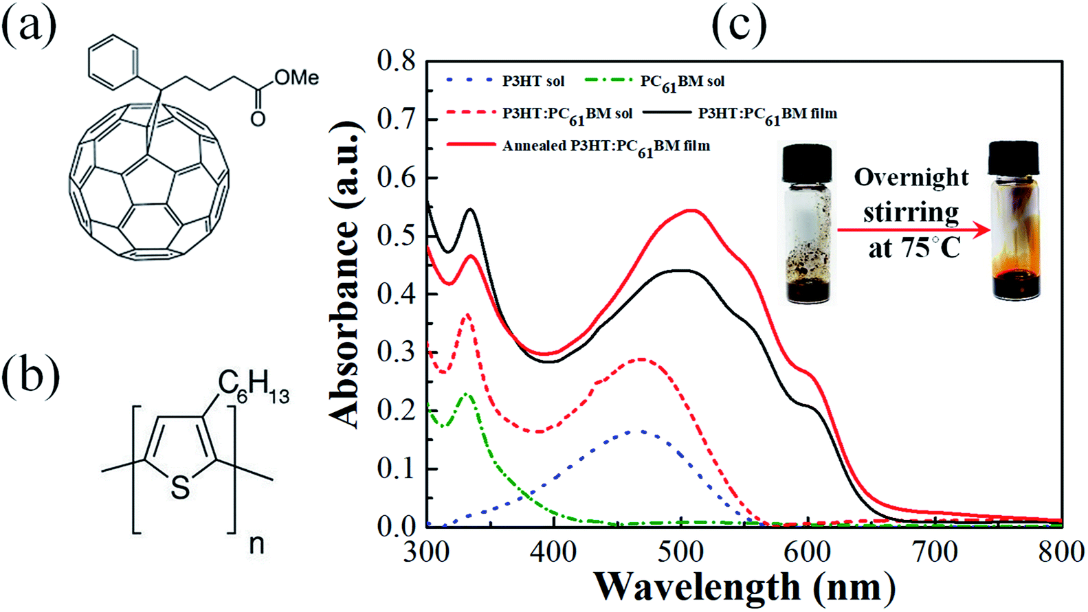 | ||
| Fig. 1 (a) and (b) Chemical structure of the PC61BM (acceptor) and P3HT (donor). (c) Absorption spectra of pristine P3HT (dotted blue line), PC61BM (dash dotted green line), P3HT:PC61BM blend (dashed red line) solution in 1,2-dichlorobenzene, pristine (solid black line) and annealed thin film of P3HT:PC61BM (solid red line) on a quartz substrate. Inset shows the optical images of the P3HT:PC61BM blend solution before and after overnight stirring at temperature 75 °C. | ||
Fig. 2(a) shows the current density–voltage (J–V) characteristics of the fabricated photovoltaic cell of structure ITO/PEDOT:PSS/P3HT:PC61BM/Al which were measured under dark and light illumination of power 100 mW cm−2 at AM 1.5G irradiation. Here, an open-circuit voltage (VOC), a short-circuit current density (JSC), fill factor (FF), and power conversion efficiency (PCE, η) of 0.5 V, 16.09 mA cm−2, 51, and 4.07%, respectively are obtained for this particular device. The external quantum efficiency (EQE) was recorded by varying wavelength in between 300 to 800 nm as shown in the Fig. 2(b). In a strong contrast, EQE values higher than 60% in between the wavelength 320 to 430 nm has been observed here which normally shows lower values for the conventional P3HT:PC61BM devices.32 The P3HT![[thin space (1/6-em)]](https://www.rsc.org/images/entities/char_2009.gif) :PC61BM blend ratio of 1:1 by weight was used to prepare active layer via spin coating which gave film thickness of ∼140 nm (ESI Fig. S1†) and maintained this for all the devices in the entire study. About 75 devices were fabricated in ambient laboratory environment with humidity level higher than 50% and at temperature ∼25 °C. The PCE (η) value as high as 4.0% has been achieved for a single junction solar cell of area 4.5 mm2. Inset of Fig. 2(b) shows the corresponding PCE statistics of 75 single-junction solar cell devices having average area of 4.5 mm2 which are classified in three different regions. A large number of devices are showing PCE value above 3% even processed and measured under ambient laboratory environment with high humidity level.33 However, JSC value and corresponding PCE has been reduced sharply for the immediate backward sweep direction than the forward one as shown in the ESI Fig. S2† which is absolutely not desirable in terms of stability.
:PC61BM blend ratio of 1:1 by weight was used to prepare active layer via spin coating which gave film thickness of ∼140 nm (ESI Fig. S1†) and maintained this for all the devices in the entire study. About 75 devices were fabricated in ambient laboratory environment with humidity level higher than 50% and at temperature ∼25 °C. The PCE (η) value as high as 4.0% has been achieved for a single junction solar cell of area 4.5 mm2. Inset of Fig. 2(b) shows the corresponding PCE statistics of 75 single-junction solar cell devices having average area of 4.5 mm2 which are classified in three different regions. A large number of devices are showing PCE value above 3% even processed and measured under ambient laboratory environment with high humidity level.33 However, JSC value and corresponding PCE has been reduced sharply for the immediate backward sweep direction than the forward one as shown in the ESI Fig. S2† which is absolutely not desirable in terms of stability.
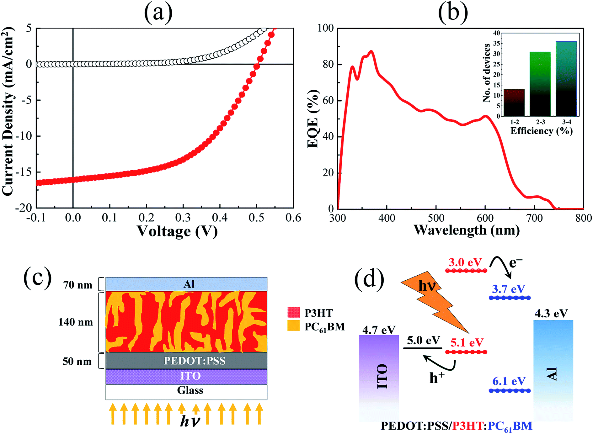 | ||
| Fig. 2 (a) Current density–voltage (J–V) characteristics of P3HT:PC61BM BHJ solar cell device in dark (black empty circles) and under white light (red filled circles) illumination of 1 sun (100 mW cm−2) simulated at AM 1.5G irradiation. (b) External quantum efficiency spectrum for a P3HT:PC61BM BHJ solar cell device. Inset shows the yield statistics of PCE (η) measurements of 75 devices with area of ∼0.045 cm2 classified with three different range of values. (c and d) Device schematic as cross-sectional view and energy-level diagram of BHJ organic solar cell of device structure ITO/PEDOT:PSS/P3HT:PC61BM/Al, respectively. | ||
Moreover, JSC value of 16.09 mA cm−2 of a single junction P3HT:PCBM solar cell is quite high compared with the values reported earlier in the literature. But the investigation for such high JSC value for these devices is out of the scope of this work. However, the higher hole mobility of P3HT polymer film due to having higher regioregularity (>98%) and purity (99.9995%) must have influence on it. This can be realised from the broad UV-vis absorption and very high EQE value towards UV region. More importantly, a solar cell simulation tool, known as GPVDM, shows a high short-circuit current density (JSC) of 19.85 mA cm−2 for the similar device structure having active layer thickness of 100 nm at the light intensity of 100 mW cm−2 as shown in the ESI Fig. S3† even the bandgaps of the used donor–acceptor are relatively high.34,35 Also, there could be some additional effects on such high JSC value like multi-exciton generation from a single photon having energy higher than the double of P3HT band gap (1.9 eV) and minimal loss of photons due to having efficient back electrode reflections.36,37 Interestingly, EQE value below 3.8 eV (326 nm) has been observed exceptionally large as shown in the Fig. 2(b) even though the sunlight intensity is too small at this region. Further, J–V characteristic under illumination of two device having different back electrode reflectance has been recorded and it shows higher JSC for the device with high back electrode reflectance as shown in ESI Fig. S4(a and b).† Reflectance of the back electrode, here Al, is important since it will effectively reduce loss of light via transmission, increase the number of photons available inside the active layer, and even increases the effective thickness almost double as reflected light passes through the active layer again.37 The schematic of actual device as a cross-sectional view is shown in Fig. 2(c). In the photoactive layer, excitons are generated in the P3HT and/or PC61BM upon light absorption and simultaneously separated across the hetero-interfaces formed between them. This charge carrier separation is favorable due to staggered gap heterojunction (type-II) formed between P3HT and PC61BM energy levels as shown in Fig. 2(d) which depict energy positions of molecular orbitals with highest occupied molecular orbital (HOMO) and the lowest unoccupied molecular orbital (LUMO) of individual components including electrodes work function.
Normally, J–V curve of a solar cell recorded in light shows three sections with different slopes to the forward bias direction. In the first region located near the zero bias where the external bias sweeps from negative to low positive voltage, the J–V curve appears as a straight line with a slope of value nearly equal to the inverse power of shunt-resistance (1/RSH). Here, the device shows the value of RSH about ∼190 Ω cm2 under light illumination which looks reasonable value in terms of OSCs. However, RSH derived from the dark current shows value ∼2.5 kΩ cm2 which is slightly less compared with the already reported results of similar device structures.38 To achieve high FF value, the conditions which lead to a decrease in RSH must be minimized. In most organic solar cells, the main source of lowering the value of RSH is the leakage current through pinholes and defects in the photoactive layer or from the edge of cells. In BHJ OSCs, leakage current has an additional path as both donor and acceptor molecule have direct contacts with each of the electrodes. Bimolecular recombination near the interface of the active layer and electrode also involve conducting leakage current. All of these should be minimized to improve the performance further. In the region up to the VOC, the slope of the J–V characteristic curve varies due to the dominance of the exponential term of diode current which determines the ideality factor (n). This ideality factors actually determines the “rectangularity” of the J–V characteristic curve under light illumination. The value of the ideality factor equal to unity is the ideal case but shows a higher value for OSCs. There is another region above the VOC where the J–V curve again appears like a straight line with a slope of about inverse power of series resistance (1/RS). Calculated series resistance value of this device was ∼10 Ω cm2 which is reasonably good. Evidently, the value of series resistance (RS) should be small enough to have a high FF. In an actual solar cell device, RS mostly appears from the contact resistance between the active layer and metal electrode. Inappropriate energy band alignment between different components can also give higher RS value and S-shaped J–V curve, causing a massive decrease in the FF and PCE.39
To ameliorate further, the effect of light intensity has been studied by varying in between 13–138 mW cm−2 at AM 1.5G irradiation on the short-circuit current density (JSC) and other performance parameters as shown in Fig. 3(a). It has been observed that the short-circuit current density (JSC) was linearly increasing with the increase of the illumination intensity. This result depicts the charge carrier generation and extraction of holes and electrons by the contacts without the presence of any energy barriers. Dependence of VOC on the illumination intensity is noticed almost invariable excluding very low-intensity region. The VOC value actually depends on the difference in energy between the LUMO of the acceptor and the HOMO of the donor. At open-circuit conditions, most of the photo-generated charge carriers recombine in the photoactive layers either by monomolecular or bimolecular mechanism.40 The Shockley–Read–Hall (SRH) mechanism states that electrons and holes prefer to recombine through trap states or recombination centers, resulting from interfacial defects and/or impurities in materials, which is known as monomolecular recombination. However, other factors also have important role in determining the VOC value, such as the potential barrier, built-in field, etc. On the other hand, the fill factor (FF) decreases with the increase of light intensity as shown in Fig. 3(a). The device showed the highest FF values at the lowest light illumination intensity. By increasing incident light intensity, the FF started decreasing and reached the lowest value. This is attributed due to the higher bimolecular recombination in the photoactive layer. Bimolecular recombination is one of the significant loss mechanism in most semiconducting conjugated polymers based solar cell devices.41 Therefore, the decrease in FF at higher light intensities showed that the FF values were heavily influenced by charge carrier recombination loss at higher light intensities. Fig. 3(a) also shows that the invariance of PCE value at higher incident light intensities which is very significant results for the ambient air processed OSCs. At intensities more than 110 mW cm−2, the PCE (η) tends to decrease slightly as observed in Fig. 3(a) which is mostly controlled by the rate of higher charge carrier recombination. Fig. 3(b) shows the dependence of device parameters on the delay time, the time required from trigger to measurement, for every data point during electrical measurements using a Keithley 2602B source measuring unit. All parameter shows lower values at greater delay time as well as at very low delay time. Only 10 ms delay time shows best performance parameters as shown in Fig. 3(b). This result shows that the measurement condition also plays an important role to produce high efficiency solar cells. This could be due to the correlated phenomena between the mobility of photo-generated charge carriers after absorbing photons from incident light and the measurement delay after triggering the bias source.
 | ||
| Fig. 3 Normalized device parameters of P3HT:PC61BM BHJ solar cell measured by varying (a) the incident light intensity and (b) the delay time (time from trigger to measurement) for current measurement by applying a particular external bias voltage using Keithley 2602B source measuring unit during voltage sweep. | ||
We also studied the effect of PEDOT:PSS thickness as the hole transporting layer (HTL) on the performance of organic solar cells, which were fabricated under ambient condition by maintaining the rest of device components unaltered. ESI Fig. S5† shows the dependence of PEDOT:PSS thickness on the spin-coating speed. Photo-induced J–V characteristics were recorded by varying the thickness ranging from 40 nm to 75 nm of HTL. Fig. 4(a) shows the J–V curve for the device with PEDOT:PSS layer thickness of 50 nm, which has given the highest JSC value as clearly depicted in the Fig. 4(b). Fig. 4(b) shows the variation of device performance parameters depending on the thickness of HTL. Ideally, there should not be any influence of HTL thickness on VOC, but a very slight fluctuation has been observed. This variation of VOC might be induced based on the variation of interface parameters between different layers during processing. Overall, the PCE was appeared maximum for the device having PEDOT:PSS thickness of 50 nm as shown in the Fig. 4(b).
 | ||
| Fig. 4 (a) A typical J–V characteristic of a device with the PEDOT:PSS layer thickness 50 nm. (b) Normalized solar cell device parameters of devices by varying the thickness of PEDOT:PSS layer. | ||
It is also obvious that the ambient processing of organic solar cells would bring down the overall price of solar panels due to reduction of the processing cost. Due to having low PCE of organic solar cells, it could be a good alternative for the low power requirement sectors. However, performance stability is an obvious desirable criteria. In this direction, the environmental stability was studied for these conventional P3HT:PC61BM devices in normal laboratory environment at temperature 25 °C and moisture level higher than 50%. Fig. 5(a) shows the normalized device parameters of an ambient air processed device as stated above which were recorded one by one in different time intervals from 0 to 120 hours. During this test, the device was kept inside a metallic chamber with electrical feedthrough and quartz window which was connected to a dynamic vacuum line maintained by the rotary vane pump which can create a vacuum level of ∼0.1 torr to minimize the other hazards. It is observed from Fig. 5(a) that the JSC decreases to almost 15% of its initial value after 120 hours of initial test. Importantly, the dropping rate of JSC was rapid at the beginning which indicates the rapid degradation of device components if exposed in ambient environment immediate after fabrication. However, it is a real challenge to fabricate the OSCs under an ambient atmosphere in a laboratory that can show a high PCE while maintaining excellent performance stability in different environmental conditions. It is already reported that prolonged exposure to humid air rapidly reduces the performance of un-encapsulated conventional devices. Various mechanisms are previously proposed to explain this decay with time. Firstly, moisture and oxygen can diffuse into the active layer via grain boundaries and defects in the metal electrode, which mainly degrades the photoactive donor polymer. However, the efficient detection techniques for such defects present in the active layer are still rare. Secondly, the top aluminum electrode can penetrate inside the top portion of active layer due to having direct contact, which can react and alter the intrinsic properties of the semiconducting donor–acceptor layer as well as can reduce the overall film thickness. However, the most severe problem causing the device instability is the fast oxidation probability of the Al electrode in ambient.42
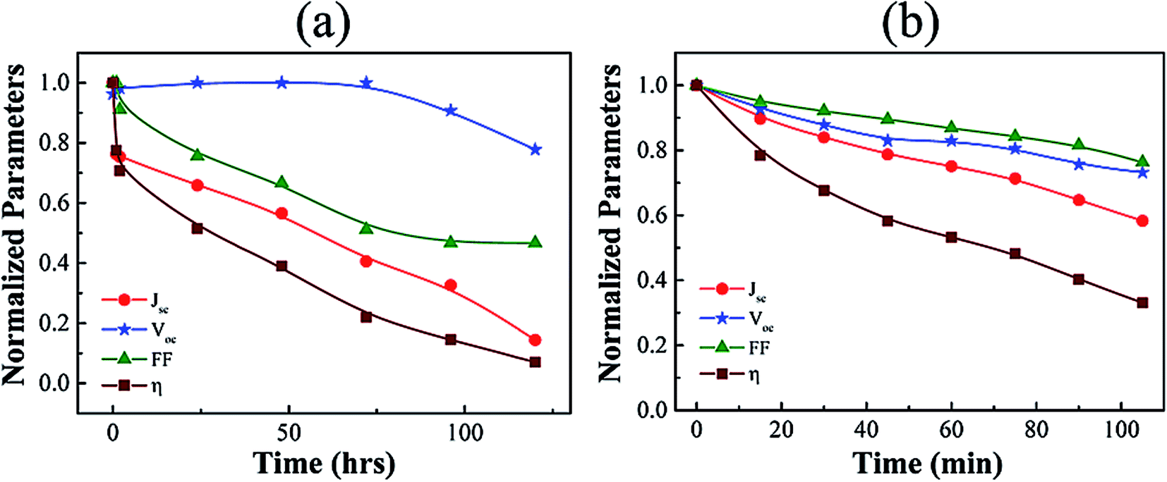 | ||
| Fig. 5 (a) Stability of normalized device parameters of a P3HT:PC61BM solar cell measured with time. (b) Similar stability test like (a) under continuous illumination. | ||
The stability of device performance parameters under continuous illumination of intensity 1 sun (100 mW cm−2) at AM1.5G is also examined as shown in Fig. 5(b). It has been observed from this study that all the performance parameters show a gradual decrease with the time under continuous illumination stress. VOC and FF show better stability compared to the JSC and PCE (η). Both the VOC and FF drop down to 80% of its initial value after 100 minute continuous illumination. Simultaneously, JSC and PCE (η) reached 60% and 40%, respectively from their starting value after 100 minutes of exposure of light intensity of 1 sun. Importantly, it has been observed that the degradation of device parameters with the time of continuous illumination was much faster than the typical environment induced degradation study as described above in Fig. 5(a). This decay indicates that the ambient atmosphere induced degradations were accelerated in the presence of constant light illumination. Therefore, immediate encapsulation after fabrication might be an effective route to protect from the device degradation by avoiding all unwanted environment induced reactions. Good organic materials with less environmental influence will be an alternative to improve the stability of the device processed in ambient environment.
Further, the influence of air processing on the dielectric properties of OSCs has also been studied to investigate in details. The capacitance of the ambient processed OSC devices by varying bias voltage for different frequencies ranging from 5 kHz to 1 MHz were measured as shown in Fig. 6(a) by applying an AC modulation voltage of amplitude 10 mV. It is noticed that the value of capacitance was invariant for higher frequencies, but it shows enhancement with a peak value at around +2 V for lower frequencies. Notably, the capacitance was almost invariant in the negative bias region for all frequencies and started increasing while sweeping towards positive bias direction. The device shows the highest peak capacitance of 50 nF for the lowest frequency 5 kHz at bias voltage around 2.0 V. After this point, the capacitance starts decreasing for further increase of bias voltage towards positive bias direction. The C–V curve at a lower modulation frequency can be classified into three regions as shown in Fig. 6(a). For the negative bias region, the capacitance value increases slowly when the bias voltage was sweeping towards a positive direction. When applied bias voltage reached the positive side, capacitance increased rapidly with the further increase of bias up to a specific applied voltage where peak capacitance appears. This voltage is ∼2.0 V for the modulation frequency of 5 kHz and 10 kHz. Drift controlled charge carriers are dominant in the reverse bias region, and diffusion is responsible for the forward bias region up to the peak capacitance value. Conduction is mainly controlled by the space charges limited currents (SCLC) after the C–V peak position in the forward bias region. In the SCLC region, drift is the dominant charge transport mechanism. Drift and diffusion are the two main parallel processes of charge carrier transport competing with each other. The peak in C–V appears due to the competition between these two, and its position determines the transition from the diffusion to the drift controlled region (SCLC).43 Furthermore, it has been observed from Fig. 6(a) that the capacitance becomes voltage as well as frequency independent for 500 kHz and 1 MHz of modulation frequency. This invariant capacitance indicates that the dielectric relaxation frequency of this ambient laboratory processed OSC devices lies below the 500 kHz. The capacitance above this frequency is mostly the geometrical capacitance (CG) of the solar cell device. The value of CG can be considered to extract the dielectric constant (ε) of the active material.44
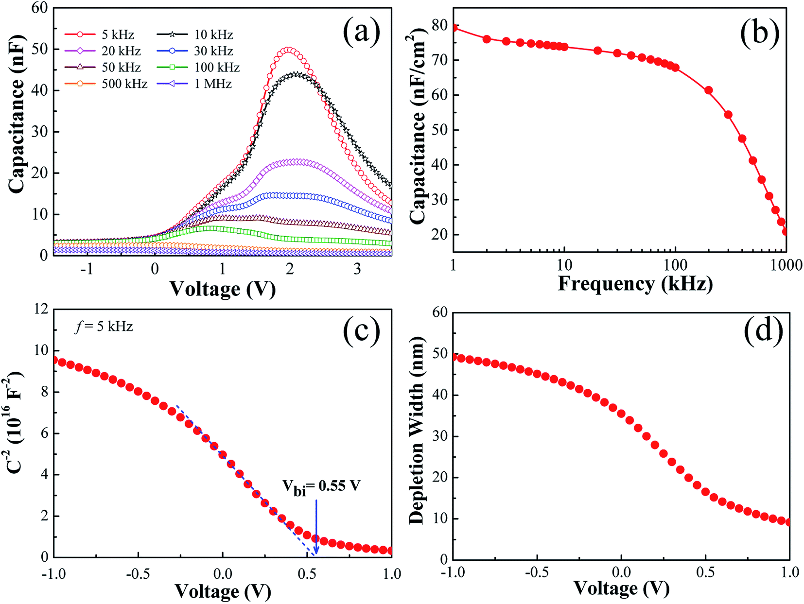 | ||
| Fig. 6 (a) Capacitance–voltage (C–V) characteristics at different frequencies by sweeping DC voltage −1.5 V to 3.5 V and (b) capacitance–frequency (C–f) characteristics by sweeping frequency 1 kHz to 1 MHz at 0 V DC bias voltage of a solar cell under dark condition. An AC voltage of amplitude 10 mV was applied to record both C–V and C–f characteristic. (c) Mott–Schottky plot (at 5 kHz) which exhibits reasonable depletion at reverse bias and linear nature at low forward bias (0.0–0.5 V). (d) Depletion width variation with bias voltage extracted from the C–V data at 5 kHz frequency. | ||
Furthermore, the frequency–dependent capacitance values (C–f) were also recorded for these devices in the range of 1 kHz to 1 MHz as shown in Fig. 6(b). In principle, there should be three capacitive regions to observe for these type of devices on the C–f curve, such as the high-frequency region for geometric capacitance, the medium frequency region for chemical capacitance, and the low frequency for static dielectric capacitance. One by one, these capacitance values appears for the respective dielectric relaxation mechanism when the corresponding relaxation process is activated in the respective separate frequency domain.45 The space charge produces an extra effect called the chemical capacitance that appears in the medium frequency range as shown in Fig. 6(b) between 1 kHz to 100 kHz. Then the capacitance value starts to decrease with the increase of frequency. However, the frequency for the onset of the particular type of capacitance depends on the resistive properties also. Therefore, a change in thickness, carrier density, and dielectric constant can produce very different results which need to be studied more for further improvement of device performance and stability.
It is intriguing to discuss here about the device performance, mainly the high JSC value of these BHJ OSC devices with the help of the impedance measurements. Basically, the C–V characteristic is related to the formation of a depletion region in the vicinity of the cathode electrode. Again, the capacitance at the reverse and low-forward bias determine the width of the depletion region, which is tuned by changing the applied voltage. Under this situation, the applied electrical field is confined near the cathode, and band bending appears with a corresponding majority-carrier depletion.46 Actually, Mott–Schottky analysis as shown in Fig. 6(c), C−2 = (2/A2qεε0NA)(Vbi − V), where V is the applied voltage, A corresponds to the device active area (0.45 mm2), q is the elementary charge, ε (=3) is the relative dielectric constant of P3HT:PC61BM film, ε0 is the permittivity of the free space, and NA is the concentration of acceptor impurities or doping level, helps to visualize such band bending in terms of Vbi (flat-band condition) extracted from the intercept of the linear region with the voltage axis and the doping level (NA) can be estimated from the C−2 − V slope. Fig. 6(c) above is yielding Vbi = 0.55 V and NA = 1.48 × 1017 cm−3.47 Here, this calculated value of the acceptor or doping level concentration corresponds to the charge density in the vicinity of the cathode electrode. Another leading aspect from Mott–Schottky analysis is that the width of the depletion region at short circuit condition w = (2εε0Vbi/qNA)1/2 which practically extends up to 35 nm from the cathode and looks much less than the active layer thickness as shown in Fig. 6(d). This is actually resulted due to the very large doping concentration (NA) which is necessary to improve the device performance including high JSC value.
Now we would like to identify the defects present in the active layer prepared in the air, which is mostly involved with solar cell device performance degradation, as discussed before. We utilized the conducting atomic force microscopy (C-AFM), which can record the topography and current image simultaneously at the same location on the photoactive P3HT:PC61BM layer. Topography image shows the RMS area roughness of 2.70 nm over (10 μm × 10 μm) area, as shown in Fig. 7(a), which is very similar compared with the film prepared inside a glove box under an inert environment.48 Surprisingly, the current image shows many white spots distributed uniformly across the whole surface, as shown in Fig. 7(b) with the peak-to-valley current span of 60.6 pA. These white spots are corresponding to the high current spikes having dimension lies between 100 nm to 500 nm, as shown in the ESI Fig. S6,† which are significantly large compared with the film thickness of 140 nm. Because of the high electron injection barrier between the conducting Pt–Ir probe and the P3HT:PC61BM layer, the electron injection is not favorable. Therefore, the current images produced here due to the hole injection only through the p-type polymer chains. Usually, the bright and dark regions should appear on the current image for the P3HT and PC61BM affluent areas, respectively. However, the high current flow has been observed at the bright regions of large diameters, which is contradicting with the area required for the high current contrast based on conventional conduction mechanism, where morphological gradients are strongly correlated to the electronic carrier energy gradient along the conductive paths.49 Therefore, it can be predicted that these bright regions of diameter more than 100 nm are defects produced on the surface of the thin film of the photoactive layer during processing.50 Hence, the current imaging is providing direct evidence about the presence of defects in the photoactive layer through which moisture or oxygen can penetrate inside the non-encapsulate device and affects the stability. Again, these defects are also not visible on the typical AFM topography image. Thus, this current imaging technique used here will be a promising tool in the future to study the defects in the photoactive layer, which will help for further process modification to reduce defects and achive higher efficiency with improved stability of BHJ organic solar cells.
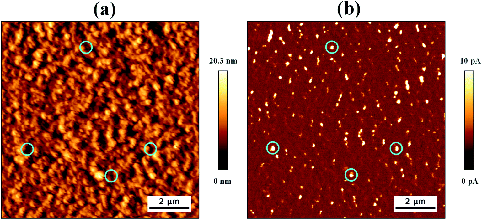 | ||
| Fig. 7 (a) and (b) Thin film topography and current image of P3HT:PC61BM on ITO/PEDOT:PSS recorded simultaneously using conducting AFM (C-AFM) measurements in contact mode at setpoint 300 mV. The scan area is (10 μm × 10 μm). | ||
3. Conclusion
In conclusion, we have successfully demonstrated bulk-heterojunction organic solar cells of conventional device structure ITO/PEDOT:PSS/P3HT:PC61BM/Al with efficiency more than 4%, which is processed and characterized entirely outside of expensive glovebox environment. Degradation was studied in ambient with aging time and under continuous light bias. Performance parameters stability is not comparable to the devices processed and characterized inside inert environment due to impose of unavoidable adverse environmental elements like oxygen or air, moisture, stray light, and so on. The dependency of solar cell parameters on delay time during J–V measurements is also observed which, needs to take care during electrical characterizations as found here. Power conversion efficiency found quite stable over the range of light intensities used in between 38 to 110 mW cm−2. Capacitance measurement by varying voltage at different frequency reveals that the drift and diffusion charge carrier transport process with transition point. Defects in the photo-active layer are identified more precisely using C-AFM through which leakage current can pass through and needs to be minimized by optimizing the fabrication steps. However, the photovoltaic performance of the devices has been seen to be consistent for several trials. Finally, the ambient processing of the organic solar cell device described here will serve to bring down the cost of fabrication and thus open up the possibilities to lower the module price.4. Experimental section
Chemicals and materials
Poly(3,4-ethylenedioxythiophene)–poly(styrene sulfonate) (PEDOT:PSS, 1 wt% in water with resistance 50–120 Ω sq.−1), poly(3-hexylthiophene-2,5-diyl) (P3HT, molecular weight = 54–75 kg mol−1, purity 99.9995%, and regioregularity > 98%), anhydrous 1,2-dichlorobenzene (purity 99%), isopropanol, and acetone (purity ≥ 99.0%) were purchased from Merck, India and used as received without further purification. Acceptor material, [6,6]-phenyl-C61-butyric acid methyl ester (PC61BM, molecular weight = 911 g mol−1 and purity > 99.5%), was purchased from Ossila Ltd, UK and used as received. ITO coated glass substrates with sheet resistance 15 Ω cm−2 were purchased from Optical Filters Inc, UK and used as transparent bottom electrode. Strips of ITO were made by etching with Zn powder and dilute hydrochloric acid (HCl). Quartz substrates used for thin film UV-vis absorption studies were purchased from Ted Pella Inc., USA. Al pellets (purity, 99.999%) were purchased from Kurt J. Lesker Company, UK for top electrode deposition. Deionized (DI) water with a resistivity of 18.2 MΩ cm was obtained from Milli-Q Direct 8 system and used for the necessary cleaning.Preparation of P3HT:PC61BM ink solution
The active layer solution of P3HT:PC61BM was prepared by mixing P3HT and PC61BM with weight ratio 1:1 in 1, 2-dichlorobenzene as described here. First, P3HT solution of concentration 20 mg ml−1 is prepared in an amber colored vial. This solution was stirred continuously for 3 hours with a magnetic stirrer at the set temperature 75 °C. An equivalent weight of PC61BM was taken as that of P3HT weight for that volume of solvent and transferred into the P3HT solution at the same 75 °C temperature with continuous stirring. This P3HT:PC61BM solution was kept for overnight stirring at 75 °C before going for spin coating over PEDOT:PSS coated ITO substrate after filtering with syringe filter having pore size 0.45 μm.
Solar cell devices fabrication
The standard organic solar cell devices of structure ITO/PEDOT:PSS/P3HT:PC61BM/Al were fabricated entirely in ambient air at ∼25 °C temperature. First, ITO on glass was patterned as strips with the help of Zn dust and dilute HCl. Briefly, we use scotch/cello tape to cover the required portion of the ITO layer on glass slide. Then, the Zn dust is used with dilute HCl to remove the uncovered ITO layer with the help of a cotton ear bud tip. This method is repeated to achieve desired pattern of ITO strips. These substrates were stored in distilled water immediately to stop further etching process. Then, these substrates were cleaned following standard protocol in laboratory detergent solution, DI water, acetone, and ethanol 3 times each for 15 minutes sequentially by ultra-sonication. Cleaned ITO substrates were dried with dry compressed air and treated with UV–ozone for 20 minutes at 95% emissivity (Holmarc, HO-TH-UVO2) before coating with PEDOT:PSS. The PEDOT:PSS solution was prepared by filtering with syringe filter having pore size 1.0 μm for spin coating over ITO. This filtered PEDOT:PSS solution was spin coated over the cleaned ITO patterned glass substrate at desired speed and time using SCS 6800 series spin coater to obtain the required thickness. In brief, 50 (±4) nm thick PEDOT:PSS layer was deposited with a two step spinning procedure, such as, 2000 rpm for 60 s followed by 4000 rpm for 60 s. Immediately, these films were annealed at 140 °C for 20 minutes on a hot plate in air. After cooling down for 15 minutes, these ITO/PEDOT:PSS films were coated with filtered P3HT:PC61BM ink solution and annealed at 130 °C for 10 minutes on hot plate in air. Here, 140 (±10) nm thick active layer was formed by following two step spinning procedure, which include 1500 rpm for 60 s followed by 3000 rpm for 60 s. Finally, aluminum (Al) top electrode of 60 (±5) nm thickness was deposited at a vacuum of about 2 × 10⁻⁶ torr using a thermal evaporator PRO Line PVD 75 procured from the Kurt J. Lesker Company, UK.Thin-film and solar cell characterizations
Electronic UV-vis absorption spectra of P3HT, PC61BM, P3HT:PC61BM ink solution in 1,2-dichlorobenzene and P3HT:PC61BM thin film on quartz substrate were measured using PerkinElmer LAMBDA 950 UV/Vis/NIR spectrophotometer. Conducting atomic force microscopy (C-AFM) based film topography, as well as simultaneous current mapping of the thin film device ITO/PEDOT:PSS/P3HT:PC61BM has been performed using JPK Nanowizard Nanoscience AFM with the help of Pt/Ir coated n-type doped Si cantilever in contact mode at set point 300 mV. Images were processed with JPK SPM data processing software. Thickness of different layers were measured using KLA-Tencor profilometer. The current density–voltage (J–V) characteristics of the devices were measured under dark and white light using a Keithley 2602B source measuring unit and KickStart 2.0 software. Solar cell performance was tested in ∼0.1 torr vacuum under simulated spectral match AM1.5G irradiation of intensity 1 sun (100 mW cm−2) using a 300 W xenon-lamp-based fiberized solar simulator (model no. SS-F5-3A) supplied by Enlitech, Taiwan. Solar simulator has been calibrated frequently with a reference cell SRC-2020 to reduce the uncertainty in light irradiance. Usually, a voltage sweeping from −1 V to +1 V was applied at ITO electrode to measure device current with respect to grounded Al electrode. The devices stored in ambient conditions were characterized for degradation and other studies for this work. EQE measurement was performed using a light source chopped at 40 Hz which is produced by combining a 250 W xenon lamp and a newport monochromator. A lock-in amplifier SRS 830 from Stanford Research System Inc., USA is used to record currents. And, a silicon photodiode calibrated by NIST has been used to identify the power of the incident light. Capacitance–voltage (C–V) and capacitance–frequency (C–f) measurements were performed using a capacitance voltage unit (4210-CVU) installed on Keithley 4200 SCS parameter analyzer. The capacitance–voltage (C–V) characteristics were recorded by sweeping bias voltage from −1.5 V to 3.5 V with an AC signal of 10 mV for different frequency ranging from 5 kHz to 1 MHz. Similarly, capacitance–frequency (C–f) characteristics were measured using an AC signal of amplitude of 10 mV between frequencies 1 kHz to 1 MHz with 0 V DC bias voltage. All the steps in the devices fabrication and characterizations were performed under ambient environment with temperature about 25 °C and humidity range 50–60%.Conflicts of interest
There are no conflicts of interest to declare.Acknowledgements
The authors acknowledge the financial support from the Indian Institute of Science Education and Research Thiruvananthapuram (IISER TVM), the Science & Engineering Research Board (SERB) (Grant No. EEQ/2016/000045 and ECR/2017/000630), and the UGC-UKIERI Joint Research Programme (UKIERI-III) (File No. 184-15/2018(IC)).References
- A. Polman, M. Knight, E. C. Garnett, B. Ehrler and W. C. Sinke, Science, 2016, 352, aad4424 CrossRef PubMed.
- S. Chu, Y. Cui and N. Liu, Nat. Mater., 2017, 16, 1C6–22 CrossRef PubMed.
- S. Y. Chang, P. Cheng, G. Li and Y. Yang, Joule, 2018, 2, 1039–1054 CrossRef CAS.
- M. T. Lloyd, J. E. Anthony and G. G. Malliaras, Mater. Today, 2007, 10, 34–41 CrossRef CAS.
- J. Y. Zhou, X. J. Wan, Y. S. Liu, G. K. Long, F. Wang, Z. Li, Y. Zuo, C. X. Li and Y. S. Chen, Chem. Mater., 2011, 23, 4666–4668 CrossRef CAS.
- S. Pfuetzner, J. Meiss, A. Petrich, M. Riede and K. Leo, Appl. Phys. Lett., 2009, 94, 223307 CrossRef.
- R. A. J. Janssen and J. Nelson, Adv. Mater., 2013, 25, 1847–1858 CrossRef CAS PubMed.
- Y. Tamai, H. Ohkita, H. Benten and S. Ito, J. Phys. Chem. Lett., 2015, 6, 3417–3428 CrossRef CAS PubMed.
- B. Siegmund, M. T. Sajjad, J. Widmer, D. Ray, C. Koerner, M. Riede, K. Leo, I. D. W. Samuel and K. Vandewal, Adv. Mater., 2017, 29, 1604424 CrossRef PubMed.
- V. Shrotriya, G. Li, Y. Yao, C. W. Chu and Y. Yang, Appl. Phys. Lett., 2006, 88, 073508 CrossRef.
- A. Tada, Y. F. Geng, Q. S. Wei, K. Hashimoto and K. Tajima, Nat. Mater., 2011, 10, 450–455 CrossRef CAS PubMed.
- W. C. Zhao, S. S. Li, H. F. Yao, S. Q. Zhang, Y. Zhang, B. Yang and J. H. Hou, J. Am. Chem. Soc., 2017, 139, 7148–7151 CrossRef CAS PubMed.
- J. Yuan, Y. Zhang, L. Zhou, G. Zhang, H. L. Yip, T. K. Lau, X. Lu, C. Zhu, H. Peng, P. A. Johnson, M. Leclerc, Y. Cao, J. Ulanski, Y. Li and Y. Zou, Joule, 2019, 3, 1140–1151 CrossRef CAS.
- Y. Kim, S. A. Choulis, J. Nelson, D. D. C. Bradley, S. Cook and J. R. Durrant, Appl. Phys. Lett., 2005, 86, 063502 CrossRef.
- H. Heil, J. Steiger, S. Karg, M. Gastel, H. Ortner, H. von Seggern and M. Stossel, J. Appl. Phys., 2001, 89, 420–424 CrossRef CAS.
- M. C. Scharber, D. Wuhlbacher, M. Koppe, P. Denk, C. Waldauf, A. J. Heeger and C. L. Brabec, Adv. Mater., 2006, 18, 789–794 CrossRef CAS.
- K. Kawano, R. Pacios, D. Poplavskyy, J. Nelson, D. D. C. Bradley and J. R. Durrant, Sol. Energy Mater. Sol. Cells, 2006, 90, 3520–3530 CrossRef CAS.
- Y. Xie, W. Huang, Q. B. Liang, J. S. Zhu, Z. Y. Cong, F. Y. Lin, S. W. Yi, G. P. Luo, T. B. Yang, S. Liu, Z. C. He, Y. Y. Liang, X. W. Zhan, C. Gao, H. B. Wu and Y. Cao, ACS Energy Lett., 2019, 4, 8–16 CrossRef CAS.
- H. T. Chien, F. Pilat, T. Griesser, H. Fitzek, P. Poelt and B. Friedel, ACS Appl. Mater. Interfaces, 2018, 10, 10102–10114 CrossRef CAS PubMed.
- M. Osaka, D. Mori, H. Benten, H. Ogawa, H. Ohkita and S. Ito, ACS Appl. Mater. Interfaces, 2017, 9, 15615–15622 CrossRef CAS PubMed.
- E. Sengupta, A. L. Domanski, S. A. L. Weber, M. B. Untch, H. J. Butt, T. Sauermann, H. J. Egelhaaf and R. Berger, J. Phys. Chem. C, 2011, 115, 19994–20001 CrossRef CAS.
- W. L. Ma, C. Y. Yang, X. Gong, K. Lee and A. J. Heeger, Adv. Funct. Mater., 2005, 15, 1617–1622 CrossRef CAS.
- S. Brixi, O. A. Melville, N. T. Boileau and B. H. Lessard, J. Mater. Chem. C, 2018, 6, 11972–11979 RSC.
- S. Sagar, A. Dey and B. C. Das, ACS Appl. Electron. Mater., 2019, 1, 2314–2324 CrossRef CAS.
- R. A. Picca, K. Manoli, E. Macchia, A. Tricase, C. Di Franco, G. Scamarcio, N. Cioffi and L. Torsi, Front. Chem., 2019, 7, 667 CrossRef CAS PubMed.
- Z. W. Jin and J. Z. Wang, Sci. Rep., 2014, 4, 5331 CrossRef CAS PubMed.
- L. G. Li, D. L. Jacobs, Y. K. Che, H. L. Huang, B. R. Bunes, X. M. Yang and L. Zang, Org. Electron., 2013, 14, 1383–1390 CrossRef CAS.
- X. N. Yang, G. H. Lu, L. G. Li and E. L. Zhou, Small, 2007, 3, 611–615 CrossRef CAS PubMed.
- K. Yuan, L. Chen and Y. W. Chen, J. Mater. Chem. C, 2014, 2, 3835–3845 RSC.
- B. Paci, G. Kakavelakis, A. Generosi, J. Wright, C. Ferrero, E. Stratakis and E. Kymakis, Sol. Energy Mater. Sol. Cells, 2017, 159, 617–624 CrossRef CAS.
- P. J. Brown, D. S. Thomas, A. Kohler, J. S. Wilson, J. S. Kim, C. M. Ramsdale, H. Sirringhaus and R. H. Friend, Phys. Rev. B: Condens. Matter Mater. Phys., 2003, 67, 064203 CrossRef.
- Y. Kim, S. A. Choulis, J. Nelson, D. D. C. Bradley, S. Cook and J. R. Durrant, Appl. Phys. Lett., 2005, 86, 063502 CrossRef.
- L. T. Dou, J. B. You, J. Yang, C. C. Chen, Y. J. He, S. Murase, T. Moriarty, K. Emery, G. Li and Y. Yang, Nat. Photonics, 2012, 6, 180–185 CrossRef CAS.
- R. C. I. MacKenzie, V. S. Balderrama, S. Schmeisser, R. Stoof, S. Greedy, J. Pallares, L. F. Marsal, A. Chanaewa and E. von Hauff, Adv. Energy Mater., 2016, 6, 1501742 CrossRef.
- R. C. I. MacKenzie, T. Kirchartz, G. F. A. Dibb and J. Nelson, J. Phys. Chem. C, 2011, 115, 9806–9813 CrossRef CAS.
- P. M. Zimmerman, Z. Y. Zhang and C. B. Musgrave, Nat. Chem., 2010, 2, 648–652 CrossRef CAS PubMed.
- Z. Tang, W. Tress and O. Inganas, Mater. Today, 2014, 17, 389–396 CrossRef CAS.
- J. R. Tumbleston, D. H. Ko, E. T. Samulski and R. Lopez, J. Appl. Phys., 2010, 108, 084514 CrossRef.
- G. del Pozo, B. Romero and B. Arredondo, Sol. Energy Mater. Sol. Cells, 2012, 104, 81–86 CrossRef CAS.
- C. M. Proctor, C. Kim, D. Neher and T. Q. Nguyen, Adv. Funct. Mater., 2013, 23, 3584–3594 CrossRef CAS.
- S. Massip, P. M. Oberhumer, G. Tu, S. Albert-Seifried, W. T. S. Huck, R. H. Friend and N. C. Greenham, J. Phys. Chem. C, 2011, 115, 25046–25055 CrossRef CAS.
- C. H. Hsieh, Y. J. Cheng, P. J. Li, C. H. Chen, M. Dubosc, R. M. Liang and C. S. Hsu, J. Am. Chem. Soc., 2010, 132, 4887–4893 CrossRef CAS PubMed.
- J. C. Nolasco, A. Sanchez-Diaz, R. Cabre, J. Ferre-Borrull, L. F. Marsal, E. Palomares and J. Pallares, Appl. Phys. Lett., 2010, 97, 013305 CrossRef.
- A. Sarkar, A. Bin Rahaman and D. Banerjee, J. Phys. D: Appl. Phys., 2018, 51, 095602 CrossRef.
- O. Almora, C. Aranda and G. Garcia-Belmonte, J. Phys. Chem. C, 2018, 122, 13450–13454 CrossRef CAS.
- P. P. Boix, G. Garcia-Belmonte, U. Munecas, M. Neophytou, C. Waldauf and R. Pacios, Appl. Phys. Lett., 2009, 95, 233302 CrossRef.
- G. Garcia-Belmonte, A. Munar, E. M. Barea, J. Bisquert, I. Ugarte and R. Pacios, Org. Electron., 2008, 9, 847–851 CrossRef CAS.
- M. Dante, J. Peet and T. Q. Nguyen, J. Phys. Chem. C, 2008, 112, 7241–7249 CrossRef CAS.
- A. C. Cefalas, Z. Kollia, N. Spyropoulos-Antonakakis, V. Gavriil, D. Christofilos, G. Kourouklis, V. V. Semashko, V. Pavlov and E. Sarantopoulou, Appl. Surf. Sci., 2017, 396, 1000–1019 CrossRef CAS.
- D. T. Duong, H. Phan, D. Hanifi, P. S. Jo, T. Q. Nguyen and A. Salleo, Adv. Mater., 2014, 26, 6069–6073 CrossRef CAS PubMed.
Footnote |
| † Electronic supplementary information (ESI) available. See DOI: 10.1039/d0ra03986a |
| This journal is © The Royal Society of Chemistry 2020 |