
 Open Access Article
 This Open Access Article is licensed under a Creative Commons Attribution-Non Commercial 3.0 Unported Licence
Heterogeneous semiconductor nanowire array for sensitive broadband photodetector by crack photolithography-based micro-/nanofluidic platforms†
Qitao Zhou‡
a,
Jun Gyu Park‡b and
Taesung Kim *b
*b
aEngineering Research Center of Nano-Geomaterials of the Ministry of Education, Faculty of Materials Science and Chemistry, China University of Geosciences, Wuhan 430074, China
bDepartment of Mechanical Engineering, Ulsan National Institute of Science and Technology (UNIST), 50 UNIST-gil, Ulsan 44919, Republic of Korea. E-mail: tskim@unist.ac.kr
First published on 22nd June 2020
Abstract
The in situ growth of nanowires (NWs) into nano-/microelectromechanical systems (NEMS/MEMS) by solution processing is attractive for its relative simplicity and economic value. We present innovative, versatile microfabrication that produces multiple, heterogeneous semiconductor NWs. A crack photolithography-based micro-/nanofluidic platform has been developed. This platform offers the in situ solution growth of NWs while enabling the control of quantity, dimensions, orientation, alignment, position, and material. The generation of grain boundary (GB)-rich CH3NH3PbI3 NWs using the micro-/nanofluidic device is exemplary. High-quality single-crystal CH3NH3PbI3 NWs were derived by injection of a CH3NH3PbI3 solution. We produced a parallel NW array of CH3NH3PbI3 NW for visible light detection and ZnO NW for ultraviolet detection, thereby demonstrating an unprecedented broadband composite photodetector. The micro-/nanofluidic fabrication platform enables the production of multiple, heterogeneous semiconductor NW arrays on one substrate, offering the potential to elicit synergistic performance and functional enhancements from various NWs.
Introduction
Semiconductor nanowires (NWs) are widely used for electronics,1 bio/chemical sensors,2 lasers,3 and photodetectors4–7 for their uniquely high surface-to-volume ratio that enables high sensitivity, rapid response time, and low power consumption.8 However, their fabrication methods typically rely on traditional micro-/nanofabrication equipment and facilities so precisely controlling the number, dimensions, orientation, alignment, and position of NWs on the same substrate9 remains a challenge. For example, chemical vapor deposition (CVD) has the general advantage of precise surface, morphology, structure, and composition control of a product, thus providing an alternative synthesis route toward high quality single-crystalline semiconductor nanowires.10,11 However it is difficult to directly use the nanowires prepared by CVD methods in the devices based on a single nanowire without manipulation and transfer. The integration of NWs into the nano-/microelectromechanical systems (NEMS/MEMS), which are integrated miniature devices that combine electrical and mechanical components at the nanoscale,12 is a significant process. The complex application of NWs in NEMS/MEMS requires a suitable fabrication process or equally advanced manipulation methods.Solution processing is a particularly desirable micro-/nanofabrication technology because of the relative simplicity and potential economy it offers.13 Solution growth of NWs usually has a high yield, but it often produces unwanted products of other morphologies.3 Nanowire manipulation is also necessary in device preparation. In situ solution processing is mainly used in film deposition processes14 rather than NWs fabrication. NW fabrication by solution processes usually requires a template or pattern that are confined to special substrates or need further transferring process.1,15 One-dimensional nanomaterials like carbon nanotubes can be self-assembled on prepatterned substrates with chemical functionalization.16 In situ growth and the control of semiconductor NWs are still difficult at low processing temperatures. The more considerable challenge is to integrate NWs comprised of different semiconductor materials into a single NEMS/MEMS while keeping processing energy consumption low in conventional micro-/nanofabrication. Such nanosystems can provide a synergistic performance and functional enhancements with multiple, heterogeneous NWs on one substrate.
NW-based photodetector optoelectronic devices have been extensively studied, but the photo response remains limited to either ultraviolet (UV) or visible light spectra.17,18 Some materials, such as perovskites, respond to both ultraviolet and visible light, but they are not very responsive in both areas at the same time.6 This limitation can easily be overcome with a photodetection NW array design that uses multiple materials with high responsivities in different wavelength ranges. Such a heterogeneous semiconductor NW based broadband photodetector based on in situ synthesis has not yet been demonstrated and reported, mainly because there are no available micro- and/or nanofabrication methods to controllably integrate such a heterogeneous semiconductor NW array in number, orientation, and material in the desired locations in a photodetector.
Here, we show an innovative, versatile microfabrication method that can produce multiple heterogeneous NWs on the same substrate. We apply the crack photolithography19 fabrication method to produce a parallel NW array of CH3NH3PbI3 NWs, a well-known organo-lead halide perovskites,20,21 and ZnO NW, thereby creating a broadband photodetector with relatively high sensitivity and responsivity. The photodetector combines the high UV response and detection ability from ZnO NWs and the high visible light response and detection ability from CH3NH3PbI3 NWs.
Results and discussion
In Fig. 1a, a schematic of the micro-/nanofluidic device containing a crack nanochannel for NW fabrication is presented. We employ crack-assisted photolithography to prepare a micro-/nanofluidic device. It facilitates the production of PDMS-based micro-/nanofluidic channel networks using standard photo- and soft lithography, as established in our previous work (see photograph in Fig. S1†).19 The scanning electron microscopy (SEM) image of a typical micro-/nanofluidic device with one central nanochannel is shown in Fig. 1b. The enlarged SEM image (Fig. 1b) and atomic force microscopy (AFM) image (Fig. 1c) indicate that the crack nanochannel is ∼2.5 μm wide and 350 nm deep. Two representative methods to fabricate a CH3NH3PbI3 NWs are performed with the assistance of our micro-/nanofluidic device.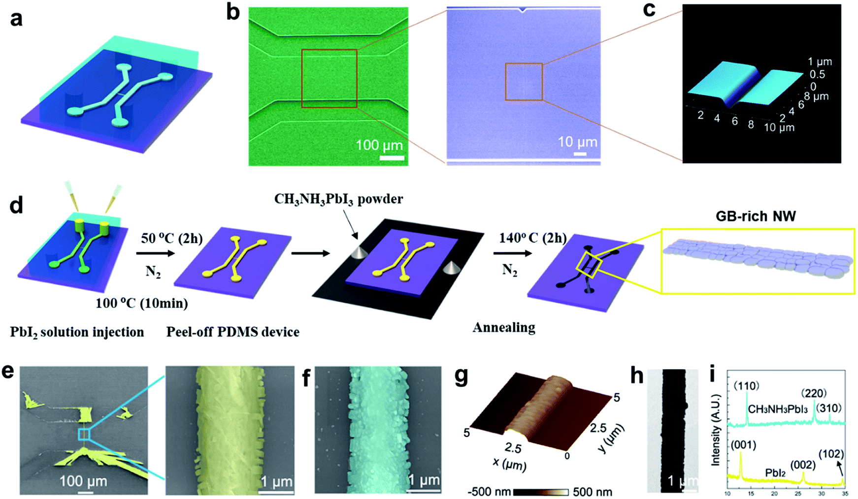 | ||
| Fig. 1 PDMS device with micro-/nanofluidic channel network and (Method-I) nanofluidic CH3NH3PbI3 NWs. (a) Schematic of the cracking-assisted micro-/nanofluidic device attached to a SiO2/Si substrate. (b) SEM image of nanowire fabrication from utilizing the nanofluidic channel; enlarged image of the crack channel. (c) AFM image of the crack nanochannel. (d) Two-step open-boundary vapor deposition method (Method-I) fabrication of CH3NH3PbI3 NWs. (e) SEM images of the single PbI2 NW made with the PDMS crack device; close-up view of the PbI2 NW. (f) CH3NH3PbI3 NW produced by further vapor deposition and annealing. (g) AFM image of the GB-rich CH3NH3PbI3 NW. (h) TEM image of the GB-rich CH3NH3PbI3 NW. (i) XRD patterns of PbI2 NW in (e) and the CH3NH3PbI3 NW formed by further vapor deposition and annealing in (f). | ||
A series of fabrication processes of CH3NH3PbI3 NWs, called the two-step and open-boundary vapor deposition method (see Experimental section) are illustrated in Fig. 1d. A PbI2 NW was synthesized by placing drops of a PbI2 solution into the micro-/nanofluidic device, followed by thermal annealing. The PbI2 was converted to CH3NH3PbI3, by exposing the PbI2 NW to CH3NH3I vapors in an N2 container. By this method, the CH3NH3PbI3 NW inherited the grain-rich structure of the PbI2 NW. An SEM image and a corresponding enlarged image of a PbI2 NW generated after the evaporation of dimethylformamide (DMF), with many small grains are shown in Fig. 1e. The chemical vapor transport reaction transmuted the PbI2 grains into CH3NH3PbI3 grains (Fig. 1f). The grain boundary (GB)-rich structure was also inherited from the PbI2 NW. AFM imaging was conducted to evaluate the dimensions of the CH3NH3PbI3 NWs. As shown in Fig. 1g, the width and height of the CH3NH3PbI3 NW were approximately 1.5 μm and 300 nm, respectively (Fig. S2a†). From the transmission electron microscopy (TEM) image in Fig. 1h, it is evident that the rough surface of the CH3NH3PbI3 NW contained many grain boundaries. The purity of phases of the PbI2 NW before and after the chemical vapor reaction were characterized by X-ray diffraction (XRD). The resulting patterns display the typical peaks of the PbI2 and CH3NH3PbI3 structures, without impurity peaks (Fig. 1i). This indicates that PbI2 was completely converted into CH3NH3PbI3.22,23
Our other fabrication process of CH3NH3PbI3 NW using the same micro-/nanofluidic device, called the one-step and closed-boundary crystallization method (see Experimental section)24 is shown in Fig. 2. For this method, a CH3NH3PbI3 solution was injected into the micro-/nanofluidic device, and the CH3NH3PbI3 NW was generated in the crack nanochannel after the evaporation of the solvent in the same N2-flooded container (Fig. 2b). The crack nanochannel appears to restrict the domain size of the CH3NH3PbI3 NW. Bulk CH3NH3PbI3 was also generated in the microchannels on one side of the crack nanochannel. The number of NWs can be controlled by the number of nanochannel in micro-/nanofluidic device. We replaced the SiO2/Si wafer substrate with a glass slide, and we monitored the real-time crystal growth process of four NWs in one device. The CH3NH3PbI3·DMF NWs crystallization occurred from the end of the nanochannel, where the lower microchannel and the nanochannel met. The NW passed through the nanochannel and continued to grow in the microchannel. The DMF in the microchannels continued to evaporate, leading to a relatively high concentration of the mixture solution within the microchannels. As a result, crystallization can continue to take place, resulting in bundles of NWs (Fig. 2c and Movie S1†). After annealing, CH3NH3PbI3·DMF NWs will be transformed into CH3NH3PbI3 NWs.
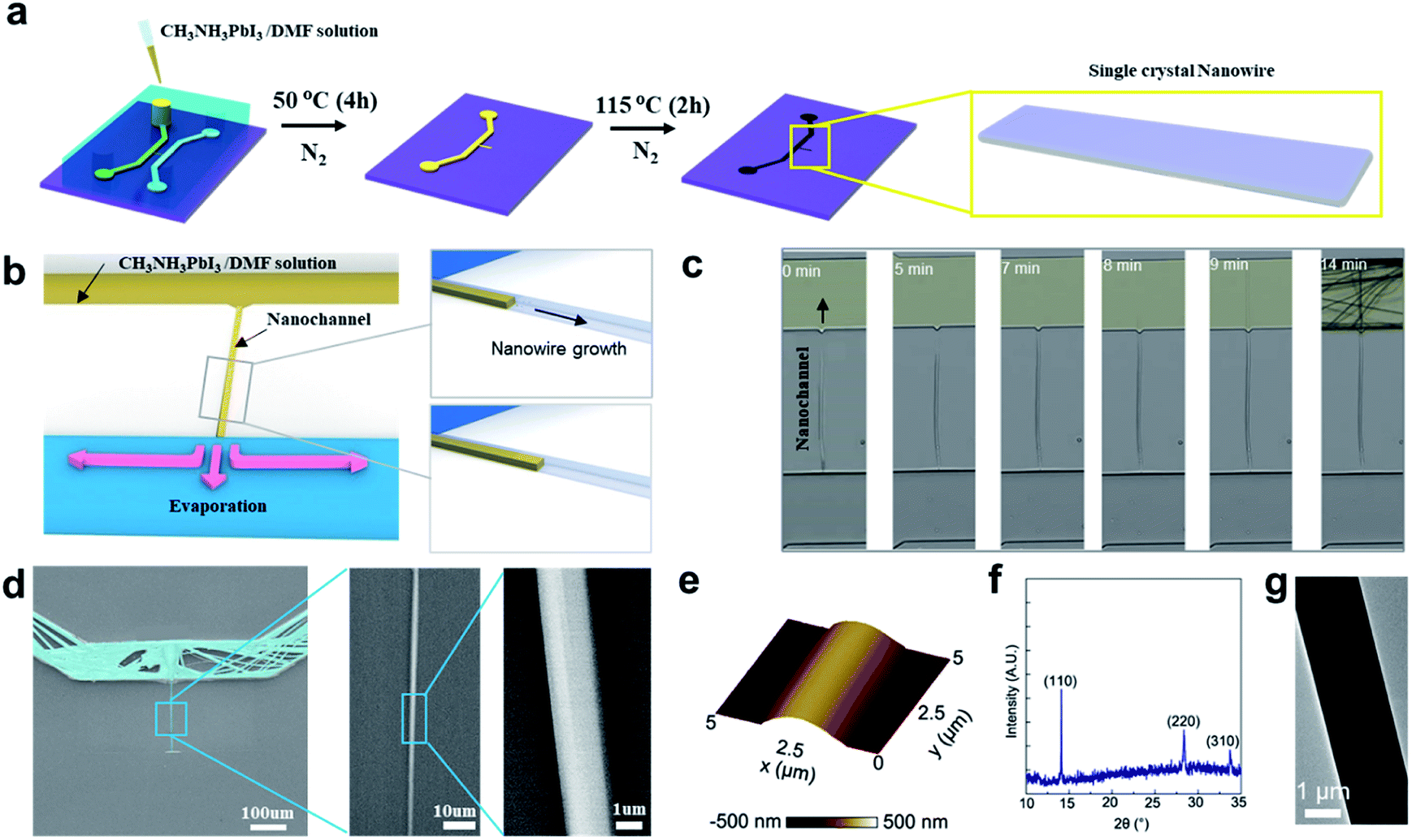 | ||
| Fig. 2 Nanofluidic fabrication process of CH3NH3PbI3 NWs (Method-II). (a) Schematic of fabrication of CH3NH3PbI3 NW by the one-step closed-boundary crystallization method (Method-II). (b) Illustration depicting the growth of a CH3NH3PbI3·DMF NW. (c) Real-time growth monitoring of a CH3NH3PbI3·DMF NW from nano- to microchannel network, filled at the upper side. (d) SEM images of the perovskite NW crack channel-restricted domain crystallization method and close-up view of the CH3NH3PbI3 NW. (e) AFM image of the single-crystal CH3NH3PbI3 NW. (f) XRD patterns of the CH3NH3PbI3 NW fabricated by Method-II and NW after air storage in darkness for 100 days. (g) TEM image of the single-crystal CH3NH3PbI3 NW. | ||
From the enlarged images in Fig. 2d, it is evident that the as-prepared CH3NH3PbI3 NW had a rather smooth surface. In the AFM image, it can be seen that the as-prepared CH3NH3PbI3 NW was arched with a width and height of 2.5 μm and 350 nm, respectively (Fig. 2e and S2b†). The XRD pattern displays the typical peaks of the perovskite structure of CH3NH3PbI3 without impurity peaks (Fig. 2f). In Fig. 2g, a typical TEM image of the CH3NH3PbI3 NW is shown, with the single-crystal characteristic demonstrated by the selected-area electron diffraction pattern from different positions for the same NW (see Fig. S3†).25
As shown in Fig. 3a, the dark-current of the GB-rich NW shows an obvious hysteresis, whereas no dark-current hysteresis could be observed for the single-crystal NW under the same test conditions (Fig. 3b) although theoretical work predicted a huge Schottky defect density of 0.4% at room temperature.26 But inconspicuous dark-current hysteresis for single-crystal NW suggests that the main reason for this phenomenon can be attributed to faster ion migration at the GBs, which has been reported in studies of both nanoscopic and macroscopic measurements.27
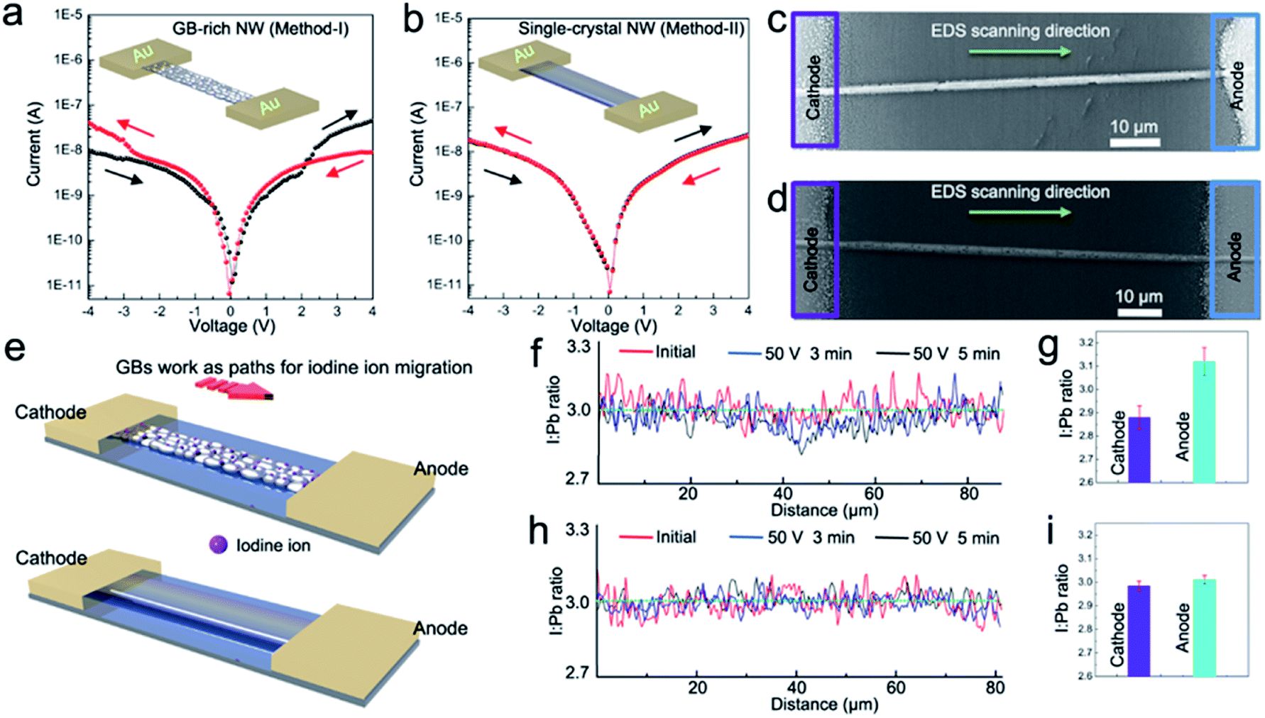 | ||
| Fig. 3 Characterization of CH3NH3PbI3 NWs fabricated using Method-I and Method-II. (a) Dark-current of a polycrystalline NW device based on single NW. (b) Dark-current of a single-crystal NW device based on a single NW. (c) SEM image of a polycrystalline NW perpendicular to two Au electrodes. (d) SEM image of a single-crystal NW perpendicular to two Au electrodes. (e) Illustration of grain boundaries working as paths for iodine ion migration. (f) I and Pb distribution along the polycrystalline NW before and after poling different durations. (g) I and Pb ratios at anode and cathode after poling for 5 min. Each error bar was calculated from five independent polycrystalline NWs (average ± std). (h) I and Pb ratio distribution along the single-crystal NW before and after poling for different durations. (i) I and Pb ratios at anode and cathode side after poling for 5 min. Each error bar was calculated from five independent single-crystal NWs (average ± std). | ||
We further investigated ion migration along long NWs with different morphologies (i.e., GB-rich polycrystalline NWs in Fig. 3c, single-crystalline NWs in Fig. 3d and schematically in Fig. 3e). The distribution of I![[thin space (1/6-em)]](https://www.rsc.org/images/entities/char_2009.gif) :Pb along the GB-rich NW before and after electrical poling is depicted in Fig. 3f. After a moderate poling of 0.5 V μm−1 was applied for 3 min at 330 K, I:Pb dropped below 3:1 near the cathode but increases above 3:1 near the anode. This tendency becomes more obvious after 2 min of additional electrical poling and is mainly attributed to the I− ionic migration and redistribution along the NW through the GBs. That is, I− ionic migration in the presence of the electric field occurs not only at long GBs of large grains but also in the entire connected GB network of small grains. No obvious change of I:Pb was observed for the single-crystalline NW before and after poling under the same experimental conditions (Fig. 3h). This can be attributed to the lack of GBs to provide paths for ion migration in the high-quality single-crystalline CH3NH3PbI3 NW. It was further confirmed by I and Pb ratios measured at the anode side and the cathode side of 5 polycrystalline NWs and 5 single-crystalline NWs after poling for 5 min (Fig. 3g and i). The quantitative analysis of ion migration was possibly limited by the relatively low accuracy of energy-dispersive X-ray spectroscopy (EDS). Still, the obtained data permits estimating the influence of GBs on ionic migration along a long NW. The result also shows that the single-crystalline NWs made by Method-II are more suitable for photodetectors than GB-rich NWs prepared by Method-I.
:Pb along the GB-rich NW before and after electrical poling is depicted in Fig. 3f. After a moderate poling of 0.5 V μm−1 was applied for 3 min at 330 K, I:Pb dropped below 3:1 near the cathode but increases above 3:1 near the anode. This tendency becomes more obvious after 2 min of additional electrical poling and is mainly attributed to the I− ionic migration and redistribution along the NW through the GBs. That is, I− ionic migration in the presence of the electric field occurs not only at long GBs of large grains but also in the entire connected GB network of small grains. No obvious change of I:Pb was observed for the single-crystalline NW before and after poling under the same experimental conditions (Fig. 3h). This can be attributed to the lack of GBs to provide paths for ion migration in the high-quality single-crystalline CH3NH3PbI3 NW. It was further confirmed by I and Pb ratios measured at the anode side and the cathode side of 5 polycrystalline NWs and 5 single-crystalline NWs after poling for 5 min (Fig. 3g and i). The quantitative analysis of ion migration was possibly limited by the relatively low accuracy of energy-dispersive X-ray spectroscopy (EDS). Still, the obtained data permits estimating the influence of GBs on ionic migration along a long NW. The result also shows that the single-crystalline NWs made by Method-II are more suitable for photodetectors than GB-rich NWs prepared by Method-I.
We characterized the CH3NH3PbI3 NWs produced by the micro-/nanofluidic fabrication platform for NW-integrated photodetectors. In Fig. S4,† the current–voltage (I–V) curves of the as-prepared CH3NH3PbI3 single-crystal NW arrays measured in the dark and under illumination are shown. We deposited two Au electrodes with a 100 μm spacing distance to connect the two ends of the NW arrays to complete a photodetector device integrated with a CH3NH3PbI3 single-crystal NW array. After measuring dark currents, we repeated the same measurement for PCs by exposing the entire device to radiation at the wavelength of λ = 532 nm and the incident light intensity of 5 mW cm−2. With the increase in the number of CH3NH3PbI3 single-crystal NWs from one to three, both the dark currents and PCs increase. The light absorption generates electron–hole pairs extracted by the source-to-drain electric field under illumination. This causes an increase in the material conductance by up to several dozen times.28 The increase from one to three CH3NH3PbI3 single-crystal NWs in the photodetectors corresponds to an increase in photosensitivity from ∼1400% to ∼2900%. Increasing the number of NWs per device is easy with our fabrication method, so it is to increase photosensitivity. Photosensitivity can also be enhanced by decreasing the bridging-gap length of 100 μm, above which the recombination of electron–hole pairs is a factor. We investigated the dark-current hysteresis and ion migration along the long NW and used the bridging-gap length of 20 μm in the photodetectors we created from here.
In Fig. 4a, a schematic of a photodetector made with our method for highly sensitive, broadband photodetection is presented. The working mechanism of the photodetector is based on two different NWs. The first ZnO NW detects UV light, and the second CH3NH3PbI3 NW detects visible light, allowing the sensing of a wide range of wavelengths. We designed a microfluidic channel network and created crack nanochannels to grow two parallel and separate NWs at a designated location on the same substrate, as shown in Fig. 4b. This micro-/nanofluidic device is placed on a SiO2/Si wafer, as shown in the microscopic image in Fig. 4b. A ZnO NW is first fabricated in the left crack nanochannel by a hydrothermal reaction29 and then a CH3NH3PbI3 NW is prepared in the right crack nanochannel by using Method-II. The ZnO NW and CH3NH3PbI3 NW are thereby successfully grown on the same substrate (Fig. 4c). The XRD pattern of the substrate displays the typical peaks of both ZnO and CH3NH3PbI3 (see Fig. S5†). An enlarged SEM image and a cross-sectional SEM image of the ZnO NW can be seen in Fig. S6.† The ZnO NW consists of small particles. Au electrodes with bridging-gap lengths of 20 μm are deposited at the ends of the two NWs. As depicted in Fig. 4a, the electrode pairs are physically separated because ZnO and CH3NH3PbI3 NW work under different bias voltages.
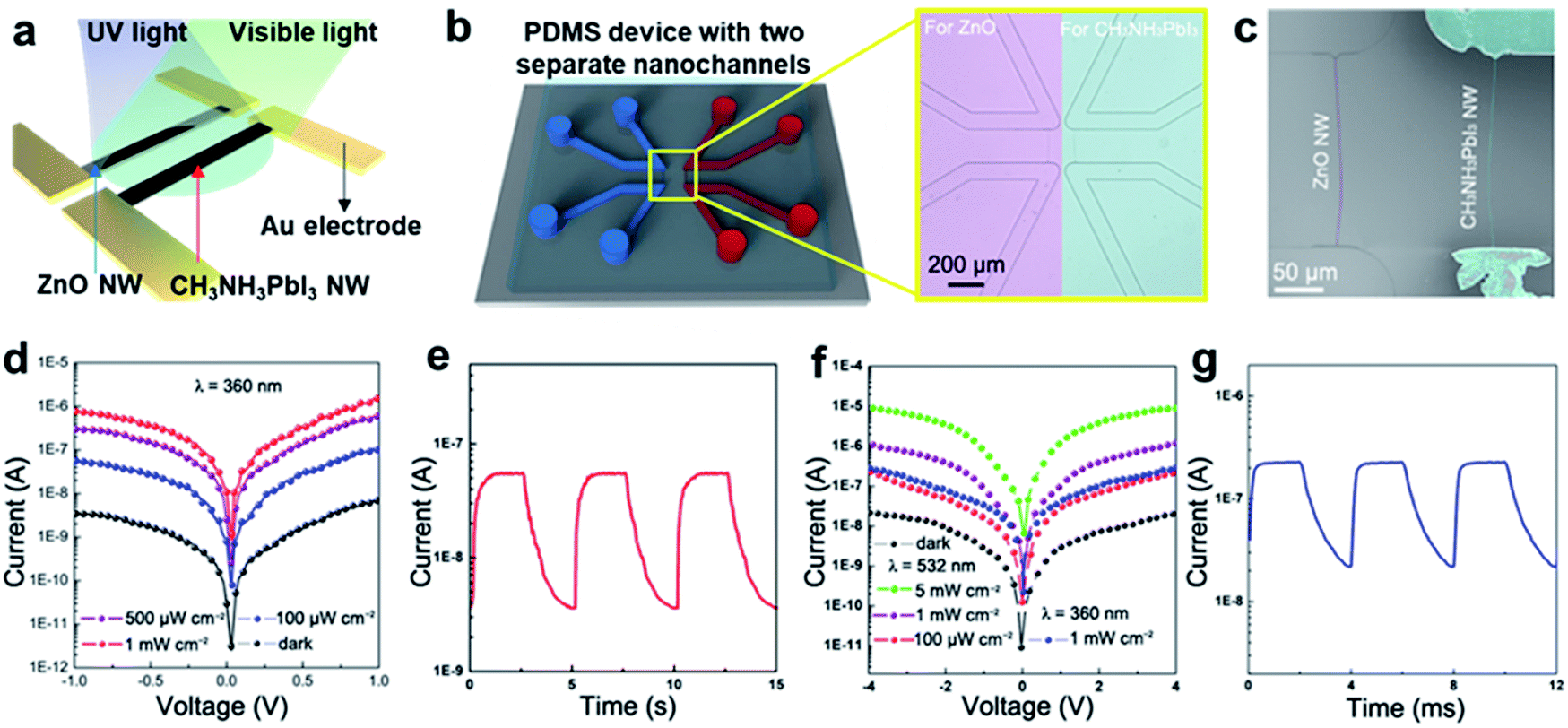 | ||
| Fig. 4 Sensitive broadband photodetector integrated with ZnO and CH3NH3PbI3 NWs in parallel. (a) Schematic of the photodetector work mechanism on two heterogeneous NWs. The ZnO NW detects UV light, CH3NH3PbI3 visible light. (b) Schematic of the PDMS micro-/nanofluidic device with two separate nanochannels. On the right is the microscopic image of the micro-/nanofluidic device with two independent, parallel crack nanochannels. (c) SEM images of the parallel ZnO NW (left) and CH3NH3PbI3 NW (right) on the same substrate and parallel to each other. (d) Dark and laser-illuminated I–V curves obtained from the ZnO NW under different illumination intensities of 360 nm light. (e) Temporal response with −1 V bias under 360 nm LED illumination with light intensities of 100 W cm−2 and a modulation frequency of 0.2 Hz. (f) Dark and laser-illuminated I–V curves obtained from the CH3NH3PbI3 NW under different illumination intensities of 532 nm and 360 nm light. (g) Temporal response with −4 V bias under 532 nm LED illumination with light intensities of 100 μW cm−2 and a modulation frequency of 250 Hz. | ||
The single ZnO NW exhibited not only ∼20000% of the dark-current photosensitivity under UV light illumination at 1 mW cm−2, as shown in Fig. 4d, but also a linear response from 20 μW cm−2 to 5 mW cm−2 (Fig. S7a†). The ZnO NW response time, defined as the time necessary for the PC to rise from 10% to 90% of the maximum, and the recovery time, defined as the time to fall the same amount, are measured as ∼0.6 s and ∼0.9 s, respectively (Fig. 4e). These times indicate a higher photo response than observed in other photodetectors utilizing ZnO nanostructures.30,31 The high surface-area-to-volume ratio of ZnO NWs can contribute to O2 re-adsorption32 as well as the generation of Schottky barriers33 between metal electrodes.
Another key figure-of-merit for photodetectors is the responsivity (R), expressed as R = Jph/Llight,34 where Jph is the PC density, and Llight is the incident light intensity. The PC density is given by Jph = Iph/S, where Iph and S are the PC and effective device area, respectively. Accordingly, R for the single ZnO NW is estimated as 1727 A W−1 under 360 nm light (1 mW cm−2) at the bias voltage of −1 V. The high PC (Iph ≈ 0.76 μA) and the small effective area (S ≈ 44 μm2, around 20 μm in length and 2.2 μm in width) of the single NW device are intrinsic and unique advantages. The figure-of-merit is even higher than that of most ZnO-nanostructure-based photodetectors (see ESI Table S1†).30,31,35,36
In Fig. 4f, the photosensitivity of the CH3NH3PbI3 NW is shown that reaches ∼6300% under 532 nm laser illumination at 1 mW cm−2 compared to the dark-current. Similarly, the CH3NH3PbI3 single NW responds linearly from 50 μW cm−2 to 50 mW cm−2 (Fig. S7b†). The response and recovery times of the single CH3NH3PbI3 NW are ∼0.28 ms and 0.92 ms, respectively (Fig. 4g), comparable to other photodetectors utilizing perovskite NWs (Table S1†).5,6,28 The R value for a single CH3NH3PbI3 NW is estimated at 275 A W−1 (Iph ≈ 0.11 μA and S ≈ 40 μm2, 20 μm in length and 2 μm in width) under 532 nm light (1 mW cm−2) at the bias voltage of −1 V, which is also impressively high.5,6,37 The R value of a single CH3NH3PbI3 NW is about 85 A W−1 (Iph ≈ 0.034 μA and S ≈ 40 μm2, 20 μm in length and 2 μm in width) under 360 nm light (1 mW cm−2) at the bias voltage of −1 V. Notably, the photosensitivity of ZnO NWs is greater than that of CH3NH3PbI3 NWs by a factor of 20 under the same UV illumination conditions, thereby overpowering the photosensitivity of CH3NH3PbI3 NWs and clearly demonstrating the synergistic advantages of combining two different semiconducting NWs in an array.
We reported in our previous work19 that crack photolithography can be used to manipulate the number, dimension, orientation, and alignment of nanoscale cracks on an SU-8 master mold. Such cracks can be recreated as a PDMS device via poly (urethane acrylate) (PUA) replication (i.e., as the second mold for PDMS). Our method easily controls important factors using standard photolithography, without nanofabrication tools and equipment. Such controllability may not be achievable in conventional nanofabrication. The limitation of this method is that only one kind of nanowire can be synthesized in turn. But our device overcomes the problem of mutual contamination in the synthesis of different NWs. Our micro-/nanofluidic fabrication method may allow a batch process for other NWs made of other materials as it can be applied to any solution processing (e.g., the syntheses for ZnS,38 TiO2,39 SnO2 (ref. 40) or metals such as Au,41 Ag,42 and Cu43). Multi-functional detectors combining differently functionalized NW sensors such as gas- and light-sensitive NWs were made.9 We, therefore, have demonstrated that our method facilitates the synthesis, alignment, and operation of NWs on various substrates in a simple, low-cost, labor-reduced, and repeatable manner.
Conclusions
We demonstrated a new NW fabrication method that produces NWs with different materials or NWs made of the same materials but exhibiting different morphologies using the same micro-/nanofluidic platform by solution process. We fabricated two types of CH3NH3PbI3 NWs with varying crystalline properties by GB richness and single crystallinity under varied processing conditions. The CH3NH3PbI3 NWs find use in photodetectors and allow an ideal material research platform to study ion migration. The proposed fabrication method enables the production of different NWs, such as ZnO NWs and CH3NH3PbI3 NWs, on the same substrate. Both solid and flexible substrate materials are permitted by using a PDMS micro-/nanofluidic device for solution loading. We demonstrated a wide-range photodetector with relatively high sensitivity to both UV light with the ZnO NW and visible light with the CH3NH3PbI3 NW made with a conventional nanofabrication process. We demonstrated only some of the capabilities of our proposed method in developing the photodetector nanosystem but thoroughly anticipate the wise spread use of our method for low-cost, large-scale, highly efficient, and flexible optoelectronic applications. Our proposed fabrication method, which allows for the control of the number, dimension, orientation, alignment, position, and material of NWs, will facilitate a variety of NW applications in the near future.Methods
Reagents and materials
A Sylgard 184 silicone elastomer kit (Dow Corning, Midland, MI, U.S.A.) was used for PDMS-based soft lithography. A polyurethane acrylate (PUA) solution, MINS-311RM, and a polyethylene terephthalate (PET) film (Minuta Tech., Osan, Korea) were used for replication of the SU-8 (SU-8 2010, MicroChem, Westborough, MA, U.S.A.) master mold. Lead(II) iodide (PbI2), methylammonium iodide (CH3NH2·HI), hexamethylenetetramine (HMTA), zinc nitrate hexahydrate (Zn(NO3)2·6H2O), isopropanol (IPA), and N,N-dimethylformamide (DMF) were purchased from Sigma Aldrich (St. Louis, MO, U.S.A.). CH3NH3PbI3 powder (CAS: 69507-98-8) was purchased from Xi'an polymer Light Technology Corp., Xi'an, Shaanxi, China. All reagents were of analytical grade and used without further purification.Fabrication of NWs using a micro-/nanofluidic platform with crack nanochannels
Two-step and open-boundary vapor deposition method (Method-I): 2 μL PbI2 DMF solution with the concentration of 0.25 M was dripped into the microchannels. After 30 min, the solution fully had filled the microchannels and the crack nanochannels by capillarity. The micro-/nanofluidic device was then heated to 50 °C and held for 30 min to evaporate the DMF. The micro-/nanofluidic device was further heated to 100 °C and held for another 10 min to altogether remove any DMF residues. The PDMS device was peeled off and removed from the SiO2/Si substrate, and then the PbI2 NWs samples were placed into a container. The container subsequently was moved into a furnace with CH3NH3I powder surrounding the substrate. Eventually, the PbI2 NWs on the substrate were converted to CH3NH3PbI3 NWs at 140 °C for 2 h.One-step and closed-boundary crystallization method (Method-II)
2 μL as-prepared CH3NH3PbI3 solution (0.5 M) was injected into the inlets of one side of two parallel PDMS microchannels. Then, the micro-/nanofluidic device was relocated into a glass container (Lock & Lock, USA) with a continuous flow of nitrogen gas as a protective gas. The glass container was placed on a hot plate and kept at 75 °C for 2 h. Lastly, the NW samples were additionally annealed at 100 °C for 1 h.ZnO NW fabrication method
Zn(NO3)2 and hexamethylenetetramine (HMTA) solutions at the concentration of 0.0025 mol L−1, respectively, were mixed to a molar ratio of 1:1. The mixture was injected into the two microchannels sandwiching one crack nanochannel. The micro-/nanofluidic device was then put on a hot plate at 90 °C and annealed for 2 h. The reaction was performed in a container in high humidity to limit the evaporation of the solutions through the PDMS device. During the entire process, the inlets and outlets of the microchannels were protected by tape to block any contamination.
Characterization and measurements of photo response of NWs
The growth process was recorded at a rate of 1 frame per 6 seconds from the beginning of injection of CH3NH3PbI3 solution to monitor the entire growth of CH3NH3PbI3 NW at 25 °C. The structural properties of our fabricated NWs were evaluated with AFM, DI-3100 (Veeco, New York, NY, U.S.A.), high resolution transmission electron microscopy (HR-TEM, JEM2100F, JEOL, Tokyo, Japan), X-ray diffraction (XRD, D8 Advance, Bruker AXS, Billerica, MA, U.S.A.), and field effect SEM (FE-SEM, S-4800, Hitachi, Tokyo, Japan), and EDS, (EMAX, Mahwah, NJ, U.S.A.). Electrical measurements of the photodetector nanosystems were conducted with a semiconductor characterization system (Model 4200, Keithley, Cleveland, OH, U.S.A.). Monochromatic light in the UV-vis range was obtained by filtering the white light from a high-power xenon lamp with optical filters, and a light intensitometer was used to determine the light intensity. A home-built measurement system that combined a laser diode (360 nm, 532 nm) and a pulse generator was used to quantify the photo response time of the photodetector nanosystems under differently pulsed light illumination conditions.Conflicts of interest
There are no conflicts to declare.Acknowledgements
This work was supported by the National Research Foundation of Korea (NRF) grant funded by the Korean government (MSIP) (NRF-2017R1A2A1A17069723, NRF-2020R1A2C3003344, and NRF-2020R1A4A2002728). The microfabrication and analyses were performed using the UNIST Central Research Facilities.References
- B. Sciacca, J. van de Groep, A. Polman and E. C. Garnett, Adv. Mater., 2016, 28, 905–909 CrossRef CAS PubMed.
- M.-J. Song, S. W. Hwang and D. Whang, J. Appl. Electrochem., 2010, 40, 2099–2105 CrossRef CAS.
- H. Zhu, Y. Fu, F. Meng, X. Wu, Z. Gong, Q. Ding, M. V. Gustafsson, M. T. Trinh, S. Jin and X. Zhu, Nat. Mater., 2015, 14, 636–642 CrossRef CAS PubMed.
- X. Liu, X. Liu, J. Wang, C. Liao, X. Xiao, S. Guo, C. Jiang, Z. Fan, T. Wang, X. Chen, W. Lu, W. Hu and L. Liao, Adv. Mater., 2014, 26, 7399–7404 CrossRef CAS PubMed.
- E. Horváth, M. Spina, Z. Szekrényes, K. Kamarás, R. Gaal, D. Gachet and L. Forró, Nano Lett., 2014, 14, 6761–6766 CrossRef PubMed.
- W. Deng, X. Zhang, L. Huang, X. Xu, L. Wang, J. Wang, Q. Shang, S.-T. Lee and J. Jie, Adv. Mater., 2016, 28, 2201–2208 CrossRef CAS PubMed.
- Y. Zhang, Y. Wang, Z.-Q. Xu, J. Liu, J. Song, Y. Xue, Z. Wang, J. Zheng, L. Jiang, C. Zheng, F. Huang, B. Sun, Y.-B. Cheng and Q. Bao, ACS Nano, 2016, 10, 7031–7038 CrossRef CAS PubMed.
- X. Chen, C. K. Wong, C. A. Yuan and G. Zhang, Sens. Actuators, B, 2013, 177, 178–195 CrossRef CAS.
- T. Zhai, X. Fang, M. Liao, X. Xu and H. Zeng, Sensors, 2009, 9, 6504–6529 CrossRef CAS PubMed.
- X. Zhou, Q. Zhang, L. Gan, X. Li, H. Li, Y. Zhang, D. Golberg and T. Zhai, Adv. Funct. Mater., 2016, 26, 704–712 CrossRef CAS.
- Y. Ahn, Y. Jeong, D. Lee and Y. Lee, ACS Nano, 2015, 9, 3125–3133 CrossRef CAS PubMed.
- O. Buchnev, N. Podoliak, T. Frank, M. Kaczmarek, L. Jiang and V. A. Fedotov, ACS Nano, 2016, 10, 11519–11524 CrossRef CAS PubMed.
- Q. Chen, H. Zhou, Z. Hong, S. Luo, H.-S. Duan, H.-H. Wang, Y. Liu, G. Li and Y. Yang, J. Am. Chem. Soc., 2014, 136, 622–625 CrossRef CAS PubMed.
- D. Liu and T. L. Kelly, Nat. Photonics, 2014, 8, 133–138 CrossRef CAS.
- A. Khan, S. Lee, T. Jang, Z. Xiong, C. Zhang, J. Tang, L. J. Guo and W.-D. Li, Small, 2016, 12, 3021–3030 CrossRef CAS PubMed.
- S.-J. Han, J. Tang, B. Kumar, A. Falk, D. Farmer, G. Tulevski, K. Jenkins, A. Afzali, S. Oida and J. Ott, Nat. Nanotechnol., 2017, 12, 861–865 CrossRef CAS PubMed.
- L. Hu, J. Yan, M. Liao, H. Xiang, X. Gong, L. Zhang and X. Fang, Adv. Mater., 2012, 24, 2305–2309 CrossRef CAS PubMed.
- D. Xiang, C. Han, J. Zhang and W. Chen, Sci. Rep., 2014, 4, 4891 CrossRef CAS PubMed.
- M. Kim, D. Ha and T. Kim, Nat. Commun., 2015, 6, 6247 CrossRef CAS PubMed.
- N. J. Jeon, J. H. Noh, Y. C. Kim, W. S. Yang, S. Ryu and S. I. Seok, Nat. Mater., 2014, 13, 897–903 CrossRef CAS PubMed.
- M. Grätzel, Nat. Mater., 2014, 13, 838–842 CrossRef PubMed.
- B. Wang and T. Chen, Adv. Sci., 2015, 3, 1500262 CrossRef PubMed.
- W. Li, J. Li, L. Wang, G. Niu, R. Gao and Y. Qiu, J. Mater. Chem. A, 2013, 1, 11735–11740 RSC.
- Q. Zhou, J. G. Park, R. Nie, A. K. Thokchom, D. Ha, J. Pan, S. I. Seok and T. Kim, ACS Nano, 2018, 12, 8406–8414 CrossRef CAS PubMed.
- N. Cho, F. Li, B. Turedi, L. Sinatra, S. P. Sarmah, M. R. Parida, M. I. Saidaminov, B. Murali, V. M. Burlakov, A. Goriely, O. F. Mohammed, T. Wu and O. M. Bakr, Nat. Commun., 2016, 7, 13407 CrossRef CAS PubMed.
- C. Eames, J. M. Frost, P. R. F. Barnes, B. C. O'Regan, A. Walsh and M. S. Islam, Nat. Commun., 2015, 6, 7497 CrossRef CAS PubMed.
- Y. Shao, Y. Fang, T. Li, Q. Wang, Q. Dong, Y. Deng, Y. Yuan, H. Wei, M. Wang and A. Gruverman, Energy Environ. Sci., 2016, 9, 1752–1759 RSC.
- P. Zhu, S. Gu, X. Shen, N. Xu, Y. Tan, S. Zhuang, Y. Deng, Z. Lu, Z. Wang and J. Zhu, Nano Lett., 2016, 16, 871–876 CrossRef CAS PubMed.
- Y. Qin, R. Yang and Z. L. Wang, J. Phys. Chem. C, 2008, 112, 18734–18736 CrossRef CAS.
- S.-M. Peng, Y.-K. Su, L.-W. Ji, C.-Z. Wu, W.-B. Cheng and W.-C. Chao, J. Phys. Chem. C, 2010, 114, 3204–3208 CrossRef CAS.
- Z. Yang, M. Wang, X. Song, G. Yan, Y. Ding and J. Bai, J. Mater. Chem. C, 2014, 2, 4312–4319 RSC.
- Y. Jin, J. Wang, B. Sun, J. C. Blakesley and N. C. Greenham, Nano Lett., 2008, 8, 1649–1653 CrossRef CAS PubMed.
- N. Liu, G. Fang, W. Zeng, H. Zhou, F. Cheng, Q. Zheng, L. Yuan, X. Zou and X. Zhao, ACS Appl. Mater. Interfaces, 2010, 2, 1973–1979 CrossRef CAS.
- L. Dou, Y. M. Yang, J. You, Z. Hong, W.-H. Chang, G. Li and Y. Yang, Nat. Commun., 2014, 5, 5404 CrossRef CAS PubMed.
- B. Nie, J.-G. Hu, L.-B. Luo, C. Xie, L.-H. Zeng, P. Lv, F.-Z. Li, J.-S. Jie, M. Feng, C.-Y. Wu, Y.-Q. Yu and S.-H. Yu, Small, 2013, 9, 2872–2879 CrossRef CAS PubMed.
- X. Liu, L. Gu, Q. Zhang, J. Wu, Y. Long and Z. Fan, Nat. Commun., 2014, 5, 4007 CrossRef CAS PubMed.
- R. Dong, Y. Fang, J. Chae, J. Dai, Z. Xiao, Q. Dong, Y. Yuan, A. Centrone, X. C. Zeng and J. Huang, Adv. Mater., 2015, 27, 1912–1918 CrossRef CAS PubMed.
- H. Zhang and L. Qi, Nanotechnology, 2006, 17, 3984–3988 CrossRef CAS.
- J.-N. Nian and H. Teng, J. Phys. Chem. B, 2006, 110, 4193–4198 CrossRef CAS PubMed.
- L. Shi and H. Lin, Langmuir, 2011, 27, 3977–3981 CrossRef CAS PubMed.
- J. Polte, R. Erler, A. F. Thunemann, S. Sokolov, T. T. Ahner, K. Rademann, F. Emmerling and R. Kraehnert, ACS Nano, 2010, 4, 1076–1082 CrossRef CAS PubMed.
- J. Zhang, X. Li, X. Sun and Y. Li, J. Phys. Chem. B, 2005, 109, 12544–12548 CrossRef CAS PubMed.
- W. Hong, J. Wang and E. Wang, Nanoscale, 2016, 8, 4927–4932 RSC.
Footnotes |
| † Electronic supplementary information (ESI) available. See DOI: 10.1039/d0ra03784b |
| ‡ These authors contributed equally to this work. |
| This journal is © The Royal Society of Chemistry 2020 |