
 Open Access Article
 This Open Access Article is licensed under a
 Creative Commons Attribution 3.0 Unported Licence
2D BeP2 monolayer: investigation of electronic and optical properties by driven modulated strain
Shivam Kansara *a,
Yogesh Sonvane*b,
P. N. Gajjarc and
Sanjeev K. Gupta*d
*a,
Yogesh Sonvane*b,
P. N. Gajjarc and
Sanjeev K. Gupta*d
aDepartment of Physics, SMMPISR, Kadi Sarva Vishwavidyalaya, Gandhinagar 382015, India. E-mail: shivam_msc@ldrp.ac.in
bAdvanced Materials Lab, Department of Applied Physics, S.V. National Institute of Technology, Surat 395007, India. E-mail: yas@phy.svnit.ac.in
cDepartment of Physics, Gujarat University, Ahmedabad 380009, India
dComputational Materials and Nanoscience Group, Department of Physics, St. Xavier's College, Ahmedabad 380009, India. E-mail: sanjeev.gupta@sxca.edu.in
First published on 17th July 2020
Abstract
Recently, the two-dimensional (2D) material beryllium diphosphide (BeP2) has attracted significant attention for potential device applications due to its Dirac semimetal state, dynamic and thermal stability, and high carrier mobility. In this work, we investigated its electronic and optical properties under biaxial Lagrangian strain using density functional theory (DFT). Electronic band gaps and effective charge carrier mass were highly sensitive to the Lagrangian strain of BeP2 monolayer. The bandgaps of BeP2 varied from 0 eV to 0.30 eV for 2% to 8% strain, where the strain range is based on the final stable condition of the system. The absorption spectra for the dielectric properties show the highest absorption peaks in the infrared (IR) region. These abundant strain-dependent studies of the BeP2 monolayer provide guidelines for its application in infrared sensors and devices.
Introduction
Strain effects in systems (metal, semiconductor, and insulator) are considered to be highly sensitive effective and convenient tools for their tuning electronic, transport, and optical properties.1–6 The applied strain effects can be interpreted as an elastic field applied to materials, which modifies the geometrical structure of their crystals due to the interaction between the elastic field and crystalline field, thus influencing the electronic band structure,7 and finally tuning the physical,8 chemical and catalytic properties9 of materials. These tools are especially reasonable for the design of two-dimensional (2D) crystals because their low-dimensional structure can sustain much larger strain compared to bulk crystals.10,11 For example, the black phosphorus (BP) monolayer has been strained up to a noteworthy value of 30% without any dislocation or plastic deformation in its crystal structure,12 giving a wide range to tune its mechanical and electronic properties.1 Besides, as a universal structure, the 2D BeP2 material with Dirac cones found precisely at the Fermi level,13 high carrier mobility and novel strain-tunable Dirac semimetal state of ultrathin BeP2 can also be altered by strain.Beryllium di-phosphide (BeP2) has attracted significant attention recently due to its Dirac semimetal state, excellent stability in the ambient environment, thermal stability, and high carrier mobility. Herein, we concentrated on a P and Be atomic sheet because Be is generally utilized as one of the constituent components in 2D binary compounds, including h-BeS,14 Be2C,15 and Be5C2.16 Besides, a BeN2 nanosheet is considered to be stable with outstanding properties due to its high stability and direct bandgap.13,17 Dirac semimetals are incredible directors of power, even though they have zero band gaps, and thus cannot be turned off. Due to the specific limitation of topology insulators in photonic devices,18,19 we applied Lagrangian strain to the BeP2 monolayer for bandgap opening. To date, there are no reports on engineering the physical and corresponding anisotropic properties of BeP2, and thus the present work focused on the examination of its in-plane anisotropic properties, including its stable structural, electrical, optical and anisotropies.
Nowadays, various researchers have focused on Dirac semimetal materials due to their rapid charge transport and significantly high carrier mobility.20–25 There are numerous reports on tuning the electronic properties of Dirac semimetal, semiconductor, and insulator monolayers for functional devices.20,23,26–36 Wang et al.26,27 reported a tunable 1T-WTe2 monolayer semimetal having a small bandgap by ambipolar conduction. Yu et al.29 reported tuning the bandgap of bilayer graphene via molecular doping with benzyl viologen molecules. Semi-metallic single-layer buckled silicene and germanene were transformed into an open bandgap using an external electric field.31 Mu et al. reported a metallic to semimetal transition with a Dirac point in BeB2 monolayer via 5% isotropic compression, while it became metallic again under a larger compression.20
In this work, the effects of strain on monolayer BeP2 were investigated using first-principles calculations. We investigated the change in the electronic and optical properties of the BeP2 monolayer under Lagrangian strain. Bandgap engineering using strain is an effective method and has been used in other 2D thin films. Besides, the strain effects on the effective mass of electrons and holes were deliberately explored.
Methodology
We have carried out ab initio DFT calculations, which were implemented using the Vienna Ab initio Simulation Package (VASP).37,38 The projector augmented wave (PAW)39 pseudopotential with the Perdew–Burke–Ernzerhof (PBE) exchange–correlation function was exploited to study the electronic properties of the semiconductor BeP2 monolayer. An orthorhombic unit cell was adopted for the planer global structure (shown in Fig. 1). Here, a vacuum spacing of greater than 16 Å was employed to prevent mirror interactions with the imaginary system in the direction perpendicular (z-axis) to the nanosheet. For the plane-wave basis set, we considered a kinetic energy cut-off of 500 eV. All structures were fully relaxed up to ionic forces less than 0.001 eV Å−1 for each atom using the conjugate gradient method from the Hellmann–Feynman theorem. The Brillouin zone (BZ) integrations were sampled using 10 × 10 × 1 and 12 × 12 × 1 special k-point sampling in the Monkhorst–Pack scheme40 for the geometry optimizations, and electronic and optical properties, respectively. The convergence criteria for the energy cut-off, k-point mesh, and smearing width were performed to reach an accuracy of total energy error less than 0.001 eV per cell. To investigate the strain effects on the atomic configuration and the electronic structure of the monolayer BeP2, we applied an external strain to the biaxial xy-axis, and allowed all atoms to freely relax. To calculate the dielectric frequency-dependent optical properties such as dielectric function, electron energy loss spectra (EELS), and reflectance and absorbance spectra, the random phase approximation (RPA) was used.41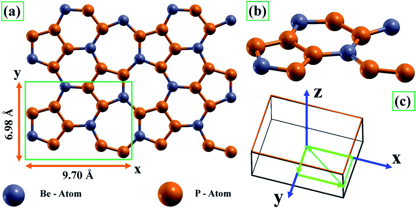 | ||
| Fig. 1 (a) Top and (b) side views of BeP2 monolayer. (a) The top view represents the 2 × 2 supercells of the BeP2 monolayer and lattice constant of the unit cell (green box). (b) Represents the diagonal view of the BeP2 monolayer (unit cell). (c) Corresponding Brillouin zone for the orthorhombic structure. | ||
Results and discussion
Structure and stability
Initially, we investigated the general structure of BeP2 to understand its properties, which are usually determined by its structure, and then studied the effect of Lagrangian strain on the structure of the BeP2 monolayer. As shown in Fig. 1(a), the supercell 2 × 2 of the BeP2 monolayer was represented by a hexagonal shape with Be and P atoms, which is consistent with other works.13 One unit cell of the BeP2 monolayer (sketched green box in Fig. 1(a)) contains four Be atoms and eight P atoms, with a calculated lattice constant (displayed in Fig. 1(a)) of 9.70 Å and 6.98 Å for the x and y-direction, respectively. Fig. 1(b) shows the side phase of the BeP2 monolayer. The corresponding path through the high symmetry points in the first Brillouin zone for the orthorhombic structure due to the electronic properties is shown in Fig. 1(c). Here, one Be atom forms a trigonal bond to an adjacent N with sp2 hybridization and no distortion. The distance between the Be and P atoms is ∼2.06 Å (varying) and P and P atoms is ∼2.09 Å (varying), as shown by in Fig. 1, which is in good agreement with a previous work.13 The explanation for the stability of the ideal BeP2 monolayer has been reported previously based on phonon spectra.13Fig. 2(a) presents the lattice constants along the x- and y-axis with different strain, which increased with an increase in strain. The variation lattice parameters affected the pressure, total energy, and binding energy of the system, which are responsible for the stability of the structure. Before investigating the various properties of the BeP2 monolayer for its potential applications, we needed to confirm its stability and feasibility for its experimental synthesis. Thus, we calculated the cohesive energy of free and strain-dependent BeP2 monolayers, as shown in Fig. 2(b). The binding energy Ebinding can be calculated as follows:
| Ebinding = EBeP2 − n(EBe − EP) | (1) |
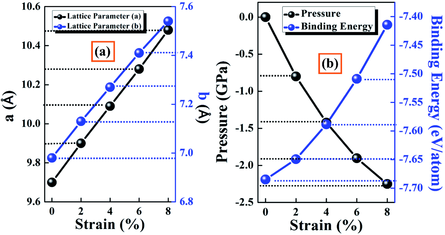 | ||
| Fig. 2 Representation of (a) lattice constants (x- and y-directions) and (b) system pressure, and binding energy per atom with various Lagrangian strain. | ||
Electronic properties
Fig. 3(a) and (b) presents the calculated band structure and partial density of states (PDOS) of a strain-free BeP2 monolayer. The curvature of the band structure of the BeP2 monolayer (Fig. 3(a)) is similar to the expected band structure of graphene, where in particular, it shows a linear Dirac-type dispersion of electrons near the X points. However, the Fermi velocity, ν, of the electrons in the BeP2 monolayer is lower than that of graphene.52 The PDOS, as shown in Fig. 3(b), demonstrates the contribution of the orbitals of the atoms. There is a larger orbital contribution from the p orbital of the atoms than the s orbital. However, the p orbital of the P atom has a larger contribution than the p orbital of the Be atom with zero density of states (DOS) at the Fermi energy, which is responsible for the semi-metallic behavior. The presented electronic properties are in very good agreement with that previously reported by Li et al.13 They have presented the orbital projected band structure, which can be used to evaluate the orbit correlation and is responsible for the semi-metallic behavior.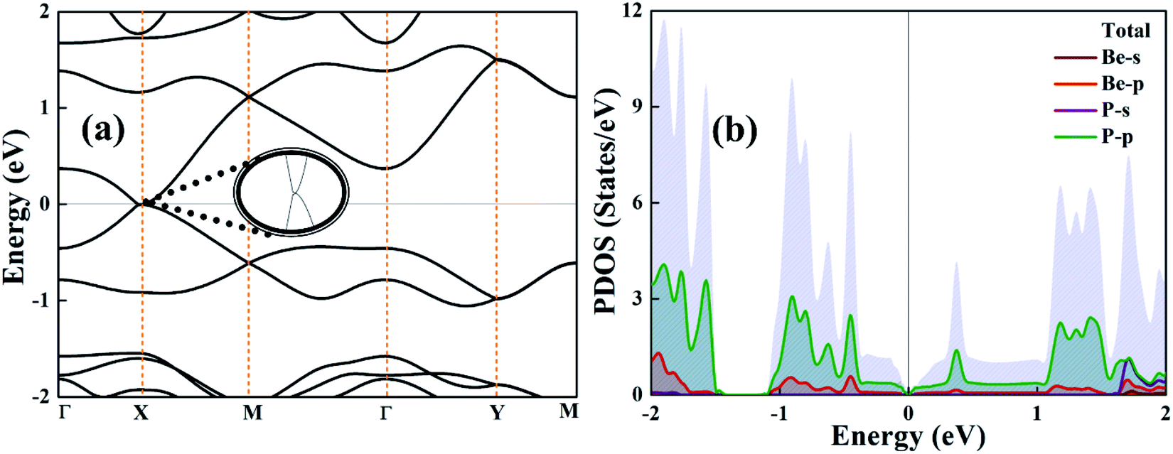 | ||
| Fig. 3 (a) Electronic band structure and (b) partial density of states (PDOS) of the BeP2 monolayer. The inset figure shows the intersection of the bands. | ||
Here, the electronic band structure and PDOS of the BeP2 monolayer under Lagrangian biaxial strain is presented in Fig. 4. For biaxial strain, the strain tensor (e) can be written as:
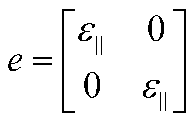 | (2) |
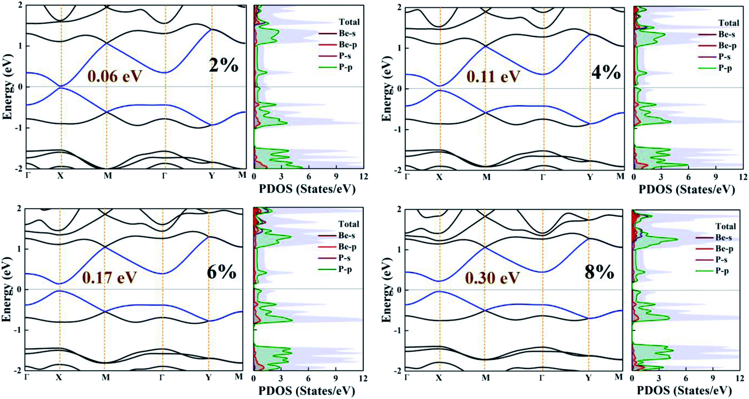 | ||
| Fig. 4 Electronic band structure and partial density of states (PDOS) of the BeP2 monolayer with various Lagrangian strain. | ||
The effect of strain on the band structures of the BeP2 monolayer is shown in Fig. 4, which was used to calculate the values of the effective masses (electron and hole), corresponding to the valence and conduction bands. The strain effect illustrates the major changes in the electronic band structure at the X-point. Thus, we can say that the conduction channel with the lowest energy and valence channel with the highest energy are located at the X-point. Direct band gaps appear at the X-point with an increase in strain, as shown in Fig. 4. Insight into the bonding character of the given monolayer was derived from the electronic charge density analysis, as shown in Fig. 5. It is clear that along the atomic sphere, the electrons are not limited, and their reasonable proportion resides in the interstitial region, thus the nature of the bonding is covalent for free strain systems. We calculated the partial density of states (PDOS) of the Be atoms and P atoms to understand their orbital contribution to the band structure. Here, the valence band mainly originates (larger contribution) from the 2p and 3p states of the Be and P atoms rather than the 2s and 3s states of the BeP2 monolayer.
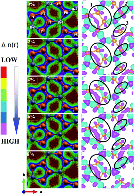 | ||
| Fig. 5 Right and left side of the electronic charge contour and electron density difference of BeP2 monolayer with various Lagrangian strain. | ||
Here, the 3p states of the P atoms form a tetrahedral contribution with the 2s states of the Be atoms. The orbital states of Be-2s and P-3p have higher orbital contributions, which are demonstrated by the higher binding energies, as shown in Fig. 2(b). The conduction and valence energy bands (i.e. CBE and VBE, respectively) shift toward a lower energy with Lagrangian tensile strain. Due to the Lagrangian strain, the band shift at the X-point corresponds to the bonding and delocalization character of the CBE and VBE orbitals, respectively. Thus, it can be concluded that Lagrangian tensile strain can successfully tune the bandgap of the BeP2 monolayer for its wide application.
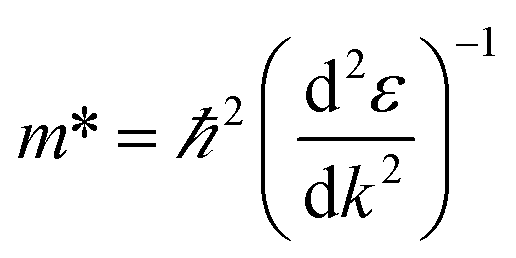
We calculated the effective masses of the electrons and holes for the band structure of the BeP2 monolayer using eqn (3) as follows:
 | (3) |
For this calculation, we used a small energy range between −0.2 eV to +0.2 eV for the conduction and valence bands near the X-point (bandgap), where the unit of the considered range ±0.2 is 2π/a (a describes the axial lattice constant). Here, the displayed band structure curve of energy versus K was fitted using the second-order polynomial ε = C1k2 + C2k + C3. According to the fitting function, we obtained the curvature  . Using the above equation and discussion, we calculated the value of the effective mass of the electrons and holes through the relation m* = ℏ2/2C1.53 The values of the effective mass of the electrons
  and holes
  are tabulated in Table 1.
| Strain (%) | 0 | 2 | 4 | 6 | 8 |
|---|---|---|---|---|---|
 |
— | 0.61 | 0.75 | 0.93 | 1.15 |
 |
— | −0.86 | −0.95 | −1.35 | −1.44 |
The energy density represents the strength or nature of bonds. The chemical bond is a concept for realizing the properties of a structure such as stability and reactivity for host materials. The calculated charge density distribution provides significant details regarding local energy density properties.54 The kinetic energy is dominant due to the positive Laplacian electron density, which is fundamental for the depletion of the bond charge. Thus, to gain deeper insight into the deformation of the BeP2 structure under Lagrangian strain, we focused on analyzing and expressing the electronic charge contour and charge difference plots in the (110) crystallographic plane, as presented in Fig. 5. The electronic charge density contour depicts the partial ionic and strong covalent bonding of the P–P and P–Be atoms based on the Pauling electronegativity difference. The atomic bonding can be observed by the color charge scale, as displayed on the right side in Fig. 5. The color charge scale represents various colors from red to pink as low electron density to high electron density, respectively. With the approach of strain, electrons are transferred from the Be to P atoms through the closest atoms. Thus, to investigate the charge transfer between two atoms of the BeP2 monolayer, the charge density difference Δρ was calculated, as illustrated in Fig. 5, using the following equation:
| Δρ = ρcomplex − ρBe − ρP | (4) |
Optical properties
Here, we presented the imaginary and real part of the frequency-dependent complex dielectric function for the BeP2 monolayer under Lagrangian strain. Investigating the optical properties of the BeP2 monolayer is important for its optoelectronic applications. The electronic band structure of materials is closely correlated to the imaginary part εi(ω), which can be represented as shown in Fig. 6(b). The transition of the interband in εi(ω) occurs from the valence band maximum (VBM) to the conduction band minimum (CBM) along the Γ–X direction and vicinity of the M-point of all the peaks. All the optical interband transitions are essentially due to the p orbital of the Be and P atoms, as shown be the PDOS in Fig. 3 and 4. Meanwhile, the real part εr(ω) represents the electronic polarizability of the material through the Clausius–Mossotti relation. The large number of peaks for the BeP2 monolayer describe the dipole-allowed transition between states near the Van Hove singularities (VHS).55 According to the literature, materials with a bandgap below 1.7 eV function outstandingly in the IR region as optical materials.56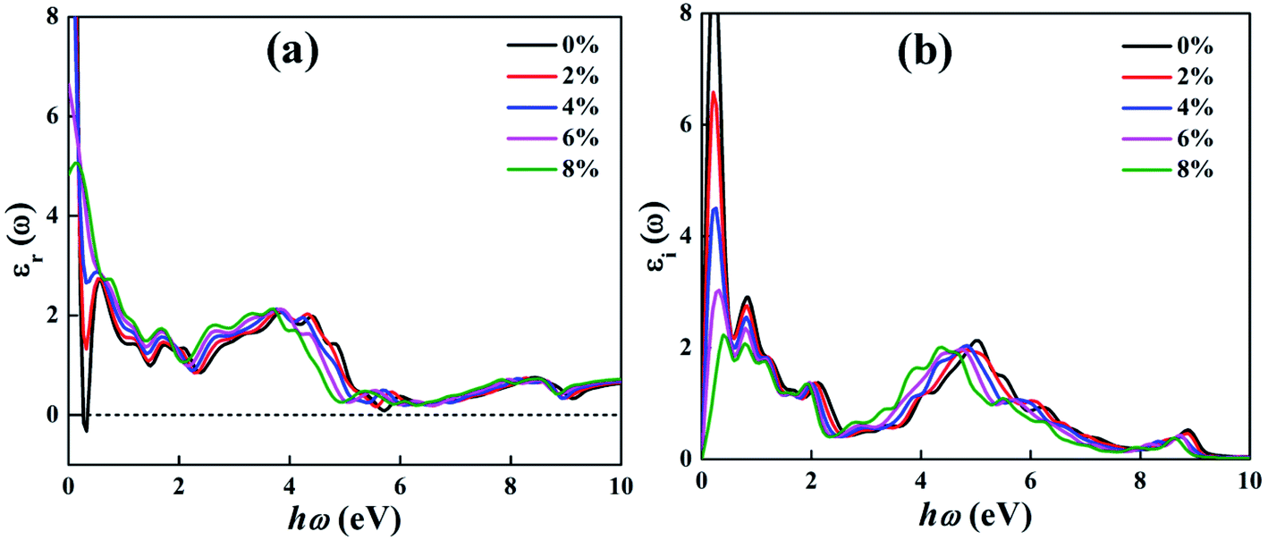 | ||
| Fig. 6 Calculated optical (a) real and (b) imaginary parts of the dielectric function of the BeP2 monolayer with various Lagrangian strain. | ||
As shown in Fig. 6(a), based on the real part of the dielectric function, we analysed the static dielectric constant at the zero frequency limits, which is 34.49, 22.37, 15.20, 6.64 and 4.82 for the 0%, 2%, 4%, 6% and 8% BeP2 monolayer, respectively, suggesting that the 0% (strain-free) BeP2 monolayer has relatively high polarizability. Also, the negative values indicate the metallic nature of the 0% (strain-free) BeP2 monolayer in the IR region. There are various peaks in the imaginary part of the dielectric function, as shown in Fig. 6(b), which is due to the electronic transitions from the 3s/3p states in the valence band to the hybridized 2p orbitals of the Be atoms and 3s/3p orbitals of the P atoms, while the last peak is due to the electronic transitions from the 2p to 3s/3p orbitals. Here, the lower and broad peaks for the dielectric properties describe the volume plasmon oscillations and the absorption of plasmon energy, respectively. As shown in Fig. 6, it can be seen that the main loss in the optical curves occurs in the range of 8–7 eV and 8.5–9.5 eV, which is due to the oscillation of the electric dipoles and the ionizing environment.
Fig. 7(a) shows the good optical efficiency in the IR range based on the low values in the EELS curve. Fig. 7(b) and (c) present the reflectivity and absorption spectra of the BeP2 monolayer for various Lagrangian strain. Here, the interband transition can be understood based on the absorption and reflection spectra of the BeP2 monolayer, while the minimum value of the reflection and absorption is observed at 2.3 eV due to the volume plasmon oscillation from 2 to 3 eV with a gap of 1 eV. Here, the absorption coefficient was calculated as A(ω) = 2ωK(ω)/C, where, K is the extinction coefficient. The maximum absorption peaks occur due to the high extinction coefficient and minimum wave transfer. According to the reflectivity in Fig. 7(b), the BeP2 monolayer is a good electromagnetic wave absorber in the absorption range of around 0 eV to 9 eV. In this absorption range, several peaks are good reflectors of UV and VIS. Table 2 presents the values of the absorption and reflection peaks and the static reflection coefficient, R(0), based on Fig. 7(b) and (c).
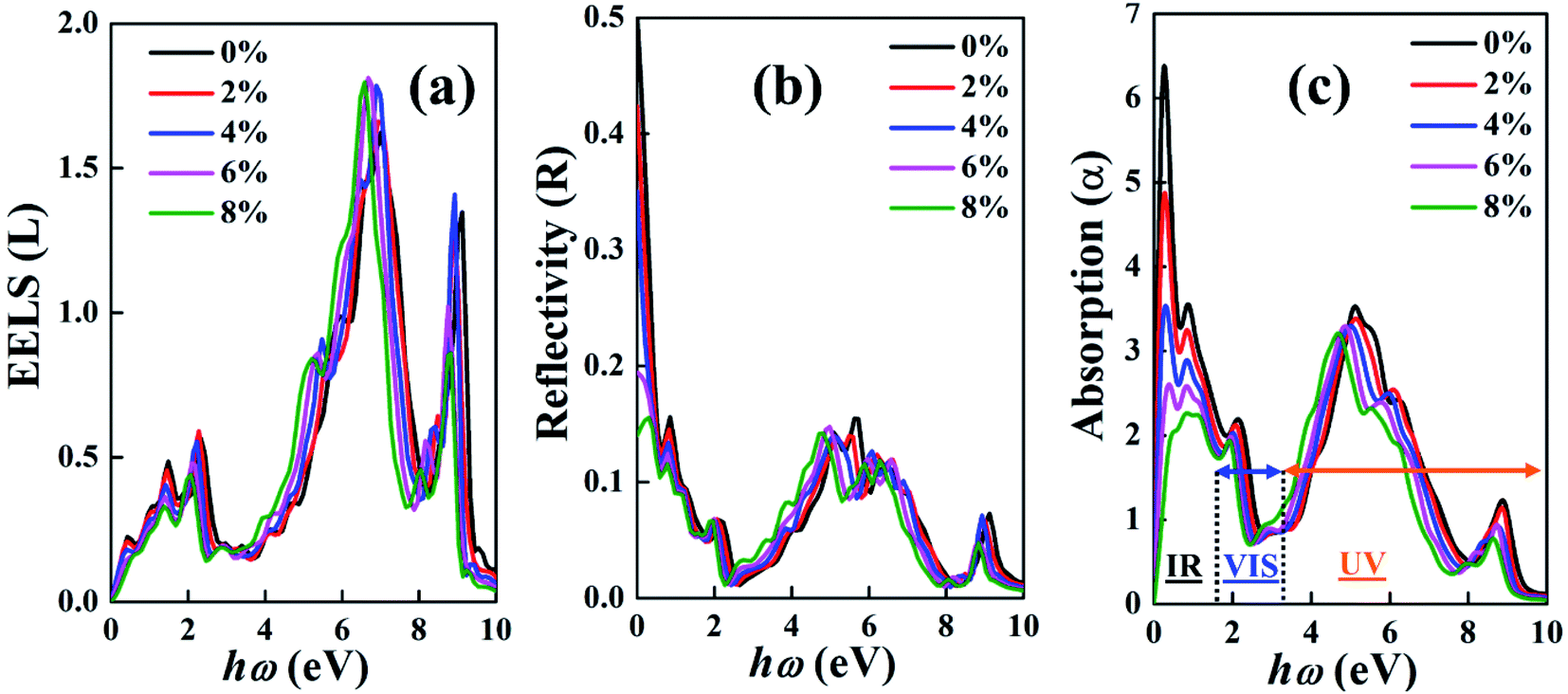 | ||
| Fig. 7 Calculated (a) electron energy loss spectrum (EELS) (L), (b) reflectivity (R) and (c) absorption spectra (α) of the dielectric function of the BeP2 monolayer with various Lagrangian strain. | ||
| Strain (%) | 0 | 2 | 4 | 6 | 8 |
|---|---|---|---|---|---|
| Absorption peaks (eV) | 2.26, 5.16, 8.81 | 2.17, 5.16, 8.80 | 2.02, 5.04, 8.72 | 1.98, 4.92, 8.76 | 1.94, 4.69, 8.61 |
| Reflection peaks (eV) | 0.86, 2.13, 5.69, 9.13 | 0.78, 2.10, 5.57, 8.98 | 0.74, 2.04, 5.08, 8.89 | 0.74, 2.0, 4.96, 8.89 | 0.74, 1.98, 4.78, 8.80 |
| R(0) | 0.50 | 0.42 | 0.35 | 0.19 | 0.14 |
By analyzing the high absorption and low EELS up to 4 eV, we can conclude that the BeP2 monolayer is an optical absorber in the IR region. The IR region has many classification names such as near IR (NIR), short-wave IR (SWIR), mid-wave IR (MWIR), and long-wave IR (LWIR) region. Due to its electric charge oscillation and ionic behavior, the maximum reflection coefficient occurs near 5.5 eV.
Conclusions
In conclusion, we used ab initio density functional theory to study the strain-dependent structural, electronic, and optical properties of the BeP2 monolayer. Accordingly, it was concluded that the stability of this system was confirmed by its cohesive energy such as 7.62, 3.48, 5.32, 3.94, 3.55 and 4.26 eV per atom and internal pressure. Upon applying tensile Lagrangian strain, the system became semiconductor in nature with direct band gaps in the range of 0.06 to 0.30 eV. Based on the dielectric function, the BeP2 nanosheets are good absorbents of electromagnetic waves in the IR region. This study is important because the bandgap is a fundamental issue that can limit the use of the emerging 2D BeP2 in the future. Thus, results present for the BeP2 nanosheets demonstrate their promising practical applications in novel mechanical–electronic devices and optical instruments such as night vision devices, thermo-graphic cameras, and infrared vibrational spectroscopy.Conflicts of interest
There are no conflicts to declare.Acknowledgements
Shivam Kansara also likes to high-performance computing clusters PARAM Shavak-C-DAC of KSV. S. K. G. would like to thank Science and Engineering Research Board (SERB), India for financial support (Grant no.: YSS/2015/001269). P. N. G. is thankful to the Department of Science and Technology, India for the support under DST-FIST and the University Grants Commission, India for the support under DRS-SAP.References
- V. Tran, R. Soklaski, Y. Liang and L. Yang, Layer-controlled band gap and anisotropic excitons in few-layer black phosphorus, Phys. Rev. B: Condens. Matter Mater. Phys., 2014, 89, 235319 CrossRef.
- J. Jiang, Q. Liang, S. Zhang, R. Meng, C. Tan, Q. Yang, X. Sun, H. Ye and X. Chen, Tuning the electronic and optical properties of graphane/silicane and fhBN/silicane nanosheets via interfacial dihydrogen bonding and electrical field control, J. Mater. Chem. C, 2016, 4, 8962–8972 RSC.
- W. Yu, C.-Y. Niu, Z. Zhu, X. Wang and W.-B. Zhang, Atomically thin binary V–V compound semiconductor: a first-principles study, J. Mater. Chem. C, 2016, 4, 6581–6587 RSC.
- M. Zhang, Y. An, Y. Sun, D. Wu, X. Chen, T. Wang, G. Xu and K. Wang, The electronic transport properties of zigzag phosphorene-like MX (M = Ge/Sn, X = S/Se) nanostructures, Phys. Chem. Chem. Phys., 2017, 19, 17210–17215 RSC.
- S. Kansara, S. K. Gupta and Y. Sonvane, Effect of strain engineering on 2D dichalcogenides transition metal: A DFT study, Comput. Mater. Sci., 2018, 141, 235–242 CrossRef CAS.
- Z. Li, X. Wang, W. Shi, X. Xing, D.-J. Xue and J.-S. Hu, Strain-engineering the electronic properties and anisotropy of GeSe2 monolayers, RSC Adv., 2018, 8, 33445–33450 RSC.
- D. Çakır, H. Sahin and F. M. Peeters, Tuning of the electronic and optical properties of single-layer black phosphorus by strain, Phys. Rev. B: Condens. Matter Mater. Phys., 2014, 90, 205421 CrossRef.
- Z. Zhang, L. Li, J. Horng, N. Z. Wang, F. Yang, Y. Yu, Y. Zhang, G. Chen, K. Watanabe and T. Taniguchi, Strain-modulated bandgap and piezo-resistive effect in black phosphorus field-effect transistors, Nano Lett., 2017, 17, 6097–6103 CrossRef CAS PubMed.
- H. Li, C. Tsai, A. L. Koh, L. Cai, A. W. Contryman, A. H. Fragapane, J. Zhao, H. S. Han, H. C. Manoharan and F. Abild-Pedersen, Activating and optimizing MoS2 basal planes for hydrogen evolution through the formation of strained sulphur vacancies, Nat. Mater., 2016, 15, 48 CrossRef CAS PubMed.
- A. S. Rodin, A. Carvalho and A. C. Neto, Strain-induced gap modification in black phosphorus, Phys. Rev. Lett., 2014, 112, 176801 CrossRef CAS PubMed.
- X. Peng, Q. Wei and A. Copple, Strain-engineered direct-indirect band gap transition and its mechanism in two-dimensional phosphorene, Phys. Rev. B: Condens. Matter Mater. Phys., 2014, 90, 085402 CrossRef.
- Q. Wei and X. Peng, Superior mechanical flexibility of phosphorene and few-layer black phosphorus, Appl. Phys. Lett., 2014, 104, 251915 CrossRef.
- X. Li and Q. Wang, Prediction of a BeP2 monolayer with a compression-induced Dirac semimetal state, Phys. Rev. B, 2018, 97, 085418 CrossRef CAS.
- J. Yu and W. Guo, Two-dimensional hexagonal beryllium sulfide crystal, J. Phys. Chem. Lett., 2013, 4, 1856–1860 CrossRef CAS PubMed.
- Y. Li, Y. Liao and Z. Chen, Be2C monolayer with quasi-planar hexacoordinate carbons: a global minimum structure, Angew. Chem., Int. Ed., 2014, 53, 7248–7252 CrossRef CAS PubMed.
- Y. Wang, F. Li, Y. Li and Z. Chen, Semi-metallic Be5C2 monolayer global minimum with quasi-planar pentacoordinate carbons and negative Poisson's ratio, Nat. Commun., 2016, 7, 11488 CrossRef CAS PubMed.
- C. Zhang and Q. Sun, A honeycomb BeN2 sheet with a desirable direct band gap and high carrier mobility, J. Phys. Chem. Lett., 2016, 7, 2664–2670 CrossRef CAS PubMed.
- X. Zhang, Q. Liu, Q. Xu, X. Dai and A. Zunger, Topological insulators versus topological Dirac semimetals in honeycomb compounds, J. Am. Chem. Soc., 2018, 140, 13687–13694 CrossRef CAS PubMed.
- Z. Fedorova, C. Jörg, C. Dauer, F. Letscher, M. Fleischhauer, S. Eggert, S. Linden and G. von Freymann, Limits of topological protection under local periodic driving, Light: Sci. Appl., 2019, 8, 1–12 CrossRef CAS PubMed.
- Y. Mu, F. Ding and H. Lu, Strain-induced metal-semimetal transition of BeB2 monolayer, RSC Adv., 2015, 5, 11392–11396 RSC.
- C. Wang, Q. Xia, Y. Nie, M. Rahman and G. Guo, Strain engineering band gap, effective mass and anisotropic Dirac-like cone in monolayer arsenene, AIP Adv., 2016, 6, 035204 CrossRef.
- K. Zhang, M. Yan, H. Zhang, H. Huang, M. Arita, Z. Sun, W. Duan, Y. Wu and S. Zhou, Experimental evidence for type-II Dirac semimetal in PtSe2, Phys. Rev. B, 2017, 96, 125102 CrossRef.
- J. Kim, S. S. Baik, S. H. Ryu, Y. Sohn, S. Park, B.-G. Park, J. Denlinger, Y. Yi, H. J. Choi and K. S. Kim, Observation of tunable band gap and anisotropic Dirac semimetal state in black phosphorus, Science, 2015, 349, 723–726 CrossRef CAS PubMed.
- H. Zhang, Y. Xie, Z. Zhang, C. Zhong, Y. Li, Z. Chen and Y. Chen, Dirac Nodal Lines and Tilted Semi-Dirac Cones Coexisting in a Striped Boron Sheet, J. Phys. Chem. Lett., 2017, 8, 1707–1713 CrossRef CAS PubMed.
- Z. Liu, J. Liu and J. Zhao, YN2 monolayer: Novel p-state Dirac half metal for high-speed spintronics, Nano Res., 2017, 10, 1972–1979 CrossRef CAS.
- L. Wang, I. Gutiérrez-Lezama, C. Barreteau, N. Ubrig, E. Giannini and A. F. Morpurgo, Tuning magnetotransport in a compensated semimetal at the atomic scale, Nat. Commun., 2015, 6, 1–7 Search PubMed.
- Y. Wang, E. Liu, H. Liu, Y. Pan, L. Zhang, J. Zeng, Y. Fu, M. Wang, K. Xu, Z. Huang, Z. Wang, H.-Z. Lu, D. Xing, B. Wang, X. Wan and F. Miao, Gate-tunable negative longitudinal magnetoresistance in the predicted type-II Weyl semimetal WTe2, Nat. Commun., 2016, 7, 1–6 CAS.
- N. D. Drummond, V. Zólyomi and V. I. Fal'ko, Electrically tunable band gap in silicene, Phys. Rev. B: Condens. Matter Mater. Phys., 2012, 85, 075423 CrossRef.
- W. J. Yu, L. Liao, S. H. Chae, Y. H. Lee and X. Duan, Toward Tunable Band Gap and Tunable Dirac Point in Bilayer Graphene with Molecular Doping, Nano Lett., 2011, 11, 4759–4763 CrossRef CAS PubMed.
- S. Zhang, Y. Zhong, Y. Li, Z. Chen and H. Zeng, Atomically Thin Arsenene and Antimonene: Semimetal–Semiconductor and Indirect–Direct Band-Gap Transitions, Angew. Chem., 2015, 127, 3155–3158 CrossRef.
- Z. Ni, Q. Liu, K. Tang, J. Zheng, J. Zhou, R. Qin, Z. Gao, D. Yu and J. Lu, Tunable Bandgap in Silicene and Germanene, Nano Lett., 2012, 12, 113–118 CrossRef CAS PubMed.
- M. Bernardi, M. Palummo and J. C. Grossman, Optoelectronic Properties in Monolayers of Hybridized Graphene and Hexagonal Boron Nitride, Phys. Rev. Lett., 2012, 108, 226805 CrossRef PubMed.
- H. Liu, Z. Huang, C. He, Y. Wu, L. Xue, C. Tang, X. Qi and J. Zhong, Strain engineering the structures and electronic properties of Janus monolayer transition-metal dichalcogenides, J. Appl. Phys., 2018, 125, 082516 CrossRef.
- R. Chaurasiya, A. Dixit and R. Pandey, Strain-driven thermodynamic stability and electronic transitions in ZnX (X = O, S, Se, and Te) monolayers, J. Appl. Phys., 2019, 125, 082540 CrossRef.
- E. M. D. Siriwardane and D. Çakir, Strain engineering of electronic and magnetic properties of double-transition metal ferromagnetic semiconductor MXenes, J. Appl. Phys., 2019, 125, 082527 CrossRef.
- M. Shi, P. Mo, J. Lu and J. Liu, Strain-enhanced electron mobility and mobility anisotropy in a two-dimensional vanadium diselenide monolayer, J. Appl. Phys., 2019, 126, 044305 CrossRef.
- G. Kresse and J. Hafner, Ab initio molecular dynamics for liquid metals, Phys. Rev. B: Condens. Matter Mater. Phys., 1993, 47, 558–561 CrossRef CAS PubMed.
- G. Kresse and J. Furthmüller, Efficient iterative schemes for ab initio total-energy calculations using a plane-wave basis set, Phys. Rev. B: Condens. Matter Mater. Phys., 1996, 54, 11169–11186 CrossRef CAS PubMed.
- G. Kresse and D. Joubert, From ultrasoft pseudopotentials to the projector augmented-wave method, Phys. Rev. B: Condens. Matter Mater. Phys., 1999, 59, 1758–1775 CrossRef CAS.
- H. J. Monkhorst, Special points for Brillouin-zone integrations, Phys. Rev. B: Solid State, 1976, 13, 5188–5192 CrossRef.
- M. Gajdoš, K. Hummer, G. Kresse, J. Furthmüller and F. Bechstedt, Linear optical properties in the projector-augmented wave methodology, Phys. Rev. B: Condens. Matter Mater. Phys., 2006, 73, 045112 CrossRef.
- K. S. Novoselov, A. K. Geim, S. V. Morozov, D. A. Jiang, Y. Zhang, S. V. Dubonos, I. V. Grigorieva and A. A. Firsov, Electric field effect in atomically thin carbon films, Science, 2004, 306, 666–669 CrossRef CAS PubMed.
- D. Singh, S. Kansara, S. K. Gupta and Y. Sonvane, Single layer of carbon phosphide as an efficient material for optoelectronic devices, J. Mater. Sci., 2018, 53, 8314–8327 CrossRef CAS.
- Y. Li, Y. Liao, P. v. R. Schleyer and Z. Chen, Al2C monolayer: the planar tetracoordinate carbon global minimum, Nanoscale, 2014, 6, 10784–10791 RSC.
- A. Fleurence, R. Friedlein, T. Ozaki, H. Kawai, Y. Wang and Y. Yamada-Takamura, Experimental Evidence for Epitaxial Silicene on Diboride Thin Films, Phys. Rev. Lett., 2012, 108, 245501 CrossRef PubMed.
- S. Kansara, S. K. Gupta, Y. Sonvane, T. Hussain and R. Ahuja, Theoretical investigation of metallic nanolayers for charge-storage applications, ACS Appl. Energy Mater., 2018, 1, 3428–3433 CrossRef CAS.
- S. Kansara, J. Shah, Y. Sonvane and S. K. Gupta, Conjugation of biomolecules onto antimonene surface for biomedical prospects: A DFT study, Chem. Phys. Lett., 2019, 715, 115–122 CrossRef CAS.
- K. Funada, A. Yamakage, N. Yamashina and H. Kageyama, Spin–Orbit-Coupling-Induced Type-I/type-II Dirac Nodal-Line Metal in Nonsymmorphic CaSb2, J. Phys. Soc. Jpn., 2019, 88, 044711 CrossRef.
- X. Han, C. Liu, J. Sun, A. D. Sendek and W. Yang, Density functional theory calculations for evaluation of phosphorene as a potential anode material for magnesium batteries, RSC Adv., 2018, 8, 7196–7204 RSC.
- J. Lee, S.-C. Lee, C. S. Hwang and J.-H. Choi, Thermodynamic stability of various phases of zinc tin oxides from ab initio calculations, J. Mater. Chem. C, 2013, 1, 6364–6374 RSC.
- F. Corsetti, P. Matthews and E. Artacho, Structural and configurational properties of nanoconfined monolayer ice from first principles, Sci. Rep., 2016, 6, 18651 CrossRef CAS PubMed.
- K. S. Novoselov, K. S. Novoselov, A. K. Geim, S. V. Morozov, D. Jiang, Y. Zhang, S. V. Dubonos, I. V. Grigorieva and A. A. Firsov, Science, 2004, 306, 666 CrossRef CAS PubMed.
- X.-H. Peng, A. Alizadeh, S. K. Kumar and S. K. Nayak, Ab initio study of size and strain effects on the electronic properties of Si nanowires, Int. J. Appl. Mech. Eng., 2009, 1, 483–499 CrossRef.
- S. Kansara, P. D. Bhuyan, Y. Sonvane and S. K. Gupta, Two-dimensional silicon phosphide: low effective mass and direct band gap for future devices applications, J. Mater. Sci., 2019, 54, 11878–11888 CrossRef CAS.
- L. Van Hove, The Occurrence of Singularities in the Elastic Frequency Distribution of a Crystal, Phys. Rev., 1953, 89, 1189–1193 CrossRef CAS.
- I. M. Baker, in Springer Handbook of Electronic and Photonic Materials, ed. S. Kasap and P. Capper, Springer International Publishing, Cham, 2017, p. 1 Search PubMed.
| This journal is © The Royal Society of Chemistry 2020 |