
 Open Access Article
 This Open Access Article is licensed under a Creative Commons Attribution-Non Commercial 3.0 Unported Licence
Tunable nanostructured distributed Bragg reflectors for III-nitride optoelectronic applications
Bin Wei†
ab,
Yingkuan Han†b,
Yanhao Wanga,
Haonan Zhaob,
Bowen Sunb,
Xiaokun Yangb,
Lin Han a,
Mingming Wangc,
Zhiyong Lid,
Hongdi Xiaob and
Yu Zhang*a
a,
Mingming Wangc,
Zhiyong Lid,
Hongdi Xiaob and
Yu Zhang*a
aInstitute of Marine Science and Technology, Shandong University, Qingdao 266237, China. E-mail: yuzhang@sdu.edu.cn
bDepartment of Microelectronics, Shandong University, Ji'nan 250100, China
cDepth Perception Institute, Jiangsu Industrial Technology Research Institute, jiangsu 214000, China
dHuaian Aucksun Optoelectronics Technology Ltd., Huai'an, 223200, China
First published on 18th June 2020
Abstract
Highly reflective and conductive distributed Bragg reflectors (DBRs) are the key for high-performance III-nitride optoelectronic devices, such as vertical cavity surface emitting lasers (VCSELs), but they still suffer from lack of lattice-matched conductive DBR and uncontrollable processes. In this work, nanostructured GaN-based DBRs were fabricated and optimized both experimentally and simulatively using electrochemical etching (EC) in different electrolytes using the transfer-matrix method (TMM) to obtain uniform wafer scale, highly reflective and conductive reflectors for the application of GaN-based optoelectronics. The results revealed that a nanostructured GaN-based DBR with high reflectivity (>93%) and broad stopband (∼80 nm) could be achieved in neutral sodium nitrate by EC, and the nanostructured GaN DBR with a full visible spectrum range could be designed by tuning the thickness of the nanostructured GaN DBR layers. The photoluminescence (PL) and light-out power enhancements of the GaN-based micro-LED by incorporating the fabricated nanostructured GaN-based DBR were 6 times and 150% without the degradation of electrical performance, respectively, which contributed to strong light scattering from the DBR layers. We believe that this work will pave a way to obtain high-performance GaN-based optoelectronic devices and guide the applications in the field of flexible devices and biomedical sensors.
1. Introduction
III-nitrides have been developed over twenty years for high-performance light emitting diodes (LEDs),1 laser diodes (LDs),2 and high-power and high-frequency power electronics3 since the first LED was reported.4 Nowadays, LEDs are indispensable in our life; GaN power electronics are on the way to practical applications in the fields of 5G (ref. 5) and fast portable chargers.6 However, GaN-based VCSEL, as an important optoelectronic device for use in the fields of displays, laser printing, and high-density optical storage, is still under development and needs further research.7 The main challenge is the absence of a suitable DBR with low strain, good conductivity, and high reflectivity for III-nitride materials. Several GaN-based DBRs have been developed, for instance, AlGaN/GaN,8 AlInN/GaN,9 and air/GaN10 or air/AlN.11 However, they suffer from either a difficult growth/fabrication process or non-conductivity. Therefore, it is still necessary to develop a strain-free, conductive nitride-based DBR.Recently, a simple technique was developed to produce single-crystal and conductive nano-porous structured GaN by using EC12 or photo-assistant electrochemical etching (PEC) processing.13 By comparison, good EC etching selectivity could be achieved by tuning the applied bias and material conductivity during the EC process,12 which provided flexibility of the design and application of the GaN nano-porous structure. Multiple applications have been demonstrated by using nano-porous structured GaN produced by the EC process, including epi-lift-off,14 chemical lift-off,15 hydrogen generation,16 gas sensors,17 biomedical applications,18 high-performance DBRs,19 LEDs,20 and laser devices.21 There are several advantages of high quality GaN-based DBR fabrication by using the EC technique: (i) perfect lattice match between GaN and the nanostructured GaN strain, resulting in almost strain-free GaN/nanostructured GaN heterostructures, (ii) reflective index (n) tunable from n = 2.5 to n = 1 by either GaN doping or applied EC bias, (iii) good conductivity of Si-doped GaN, and (iv) the orientation independent isotropic etching of GaN materials. By taking these advantages, (Al)GaN nanostructured DBRs have been obtained by using Si-doped (Al)GaN and unconventionally doped (UID) (Al)GaN alternative stacks,22–24 and incorporated into GaN-based optoelectronics, including blue LEDs21 and UV LEDs.25 However, the study of GaN/GaN nanostructured DBRs by using all Si-doped GaN layers is still lacking.
Besides, the EC process involves many parameters, such as electrolyte chemistry, applied bias, doping concentration of the semiconductor, and surface conditions, which making it very complex and difficult to control. In the literature, different parameters affecting the EC process and GaN nanostructure performance were reported, and different results were obtained. For instance, oxalic acid was used to produce nano-porous GaN with different Si-doping concentrations, and microdisk and cantilever devices were demonstrated;12 ethanol/glycerol buffered HF was used to etch Si-doped GaN by the EC process and highly reflective air/GaN DBR (>98%) was achieved with four pairs of GaN/air stack;26 HNO3 and H2SO4 electrolytes were studied and highly reflective GaN/nanoporous DBR was obtained in HNO3 by using a Si-doped GaN/UID GaN stack;27 KOH and different 1-ethyl-3-methylimidazolium-based ionic liquid electrolytes were also used to produce porous GaN under UV illumination.13,28 Among these studies, many electrolytes are highly toxic and/or corrosive, which make the (P)EC process challenging and dangerous from the technical and safety point of view. Therefore, the EC process using neutral or non-aggressive electrolytes needs to be developed/studied together with the control of each parameter for the GaN nanostructure.
In this work, the selective etching of the n+-GaN:Si/n−-GaN:Si alternative layers was studied by EC in different environment friendly electrolytes for optoelectronic application. The effects of the neutral electrolyte and applied bias were investigated in terms of the etching nanostructure morphology and the reflectivity of nanostructured GaN. The tunability of the nanostructured-GaN DBR was explored through transfer-matrix method (TMM) simulation by varying thickness and stack pairs of the nanostructured GaN layer. Finally, we demonstrated that the performance improved the micro-LED by using the developed nanostructured GaN DBR.
2. Materials and methods
GaN and GaN LED structures with GaN nanostructured DBR were grown on a 2-inch patterned sapphire substrate using a metal–organic chemical vapor deposition (MOCVD) system. The epitaxial structure consisted of a 20 nm-thick sputtered AlN and 2 μm-thick unintentionally doped (UID) GaN buffer layer, a 1 μm-thick heavily doped GaN layer (1 × 1019 cm−3) to improve the etching uniformity of the porous GaN DBR, and a stack structure of 15 pairs of n+-GaN:Si/n−-GaN:Si epitaxial layers (46 nm/1 × 1019 cm−3, 60 nm/2 × 1018 cm−3), as shown in Fig. 1(a). 46 nm/60 nm was designed to form a stopband centered at about 450 nm. For the LED structure, as shown in Fig. 1(b), a 50 nm thin UID GaN cap layer was grown on the structure shown in Fig. 1(a), followed by an n-AlGaN electron blocking layer, an InGaN/GaN (well/barrier) multilayer, and heavily Mg-doped P-GaN layer. An in situ annealing process was used to activate the p-doping of the LED structure with nitrogen flow in the MOCVD reactor.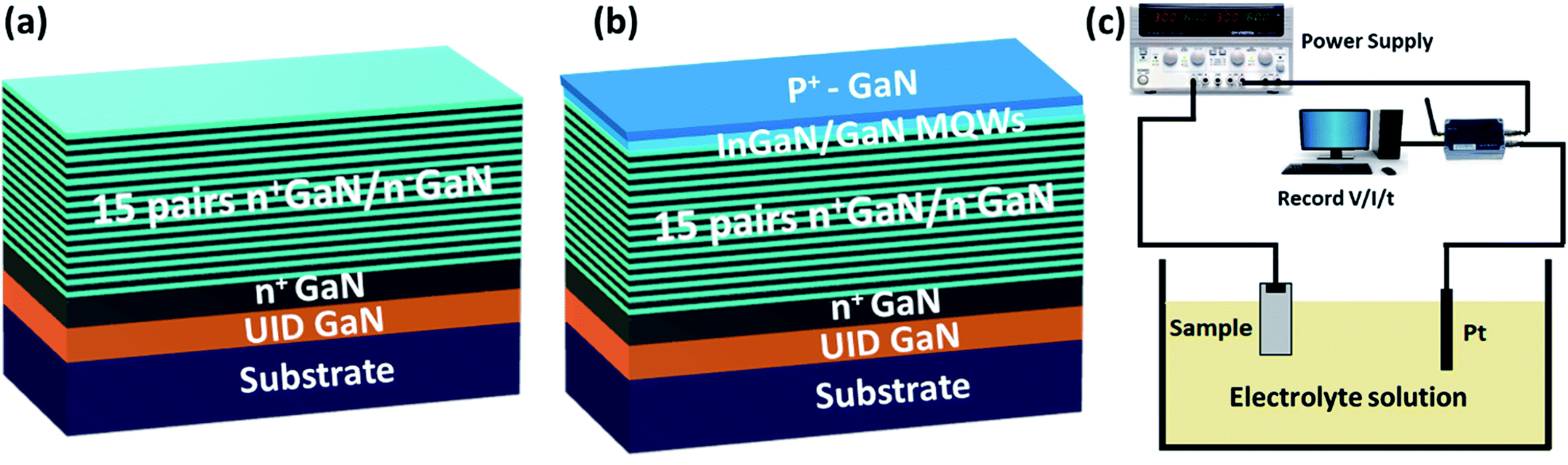 | ||
| Fig. 1 Schematic structures of the DBR (a) and LED (b) samples; (c) diagram of the electrochemical etching setup. | ||
Electrochemical etching was carried out in the setup shown in Fig. 1(c). The GaN sample and platinum wire were used as the anode and cathode, respectively. Computer controlled power meter was used to supply power and record the process current and voltage. 0.3 M oxalic acid and 0.3 M sodium nitrate were chosen as the electrolytes for studying the electrolyte-dependent doped GaN etching selectivity because they are both environment friendly. The samples were rinsed in deionized water and blow dried by using a nitrogen gun after EC processing. Ideally, n+-GaN (1 × 1019 cm−3) was transferred into high-porosity nanostructured GaN as a low refractive index layer and n−-GaN (2 × 1018 cm−3) was kept unetched or transferred into the low-porosity nanostructured GaN as the high refractive index layer during electrochemical etching. A highly reflective conductive nanostructured GaN based DBR was formed.
The LED wafer was processed to obtain rectangular LEDs of dimensions 100 × 80 μm2. The fabrication process was as follows: GaN was patterned by chlorine-based inductively coupled plasma reactive ion etching process to reach the N-type region. GaN nanostructured DBR was formed by using electrochemical etching in 0.3 M sodium nitrate. P- and N-contacts were then patterned and deposited to obtain independently addressable LEDs. After that, a silicon dioxide (SiO2) passivation layer was deposited and a lithographic step opened the P- and N-contact pads.
The top and cross-sectional micrographs of the samples were observed using a field-emission scanning electron microscope (SEM). The reflectance spectra and photoluminescence (PL) spectra were measured by using an Ideaoptics PG4000 spectrum system with a halogen light source and a 405 nm laser, respectively. The transfer-matrix method (TMM) was used to simulate the reflectivity of the nanostructured GaN DBR. The characterization of the LEDs was conducted on a semi-auto optoelectronic probe station with a 2 inch integrating sphere and a Keithley 2600 source meter.
3. Results and discussion
3.1 Morphology and reflectivity
Fig. 2 shows the top view (a) and (b) and cross-sectional (c) and (d) view SEM images and the corresponding reflectivity spectra (e) and (f) of GaN nanostructured DBR produced by electrochemical etching in 0.3 M oxalic acid electrolyte at different biases of 12 V (a, c and e) and 18 V (b, d and f), respectively. From the top SEM images of nanostructured GaN DBR, as shown in Fig. 2(a) and (b), we can see some nanoscale pores formed on the sample surface, whose the pore size is about 20–30 nm in diameter and increases with an increase in the applied bias; the pore density increases from 4.3 × 108 cm−2 to 7.6 × 108 cm−2 with an increase in the applied bias, which is comparable with the GaN defect density (∼1 × 10⁸ to 1 × 109 cm−2) grown on a sapphire substrate. These initial nanopore formations may be dislocation related EC etching.29 From the cross-sectional view SEM images of the samples, as shown in Fig. 2(c) and (d), random pores were formed throughout the whole n+-GaN/n−-GaN alternative multilayer and there is no clear interface observed for both low and high applied bias conditions. The pore size and porosity of the samples increase with an increase in the applied bias. As shown in the inset of Fig. 2(c), the nanoscale pores formed on the surface went through the top n−-GaN extending to the underlying n+-GaN layer and enabled the underlying etched layers to form random nanostructures. The reflectance spectra of the samples are shown in Fig. 2(e) and (f) and the measured reflectivity of the samples was only 63.03% and 39.31% for low (12 V) and high (18 V) applied bias conditions, respectively. This implying that the samples had a bad optical performance and oxalic acid electrolyte is not suitable for making high quality nanostructured GaN-based DBRs.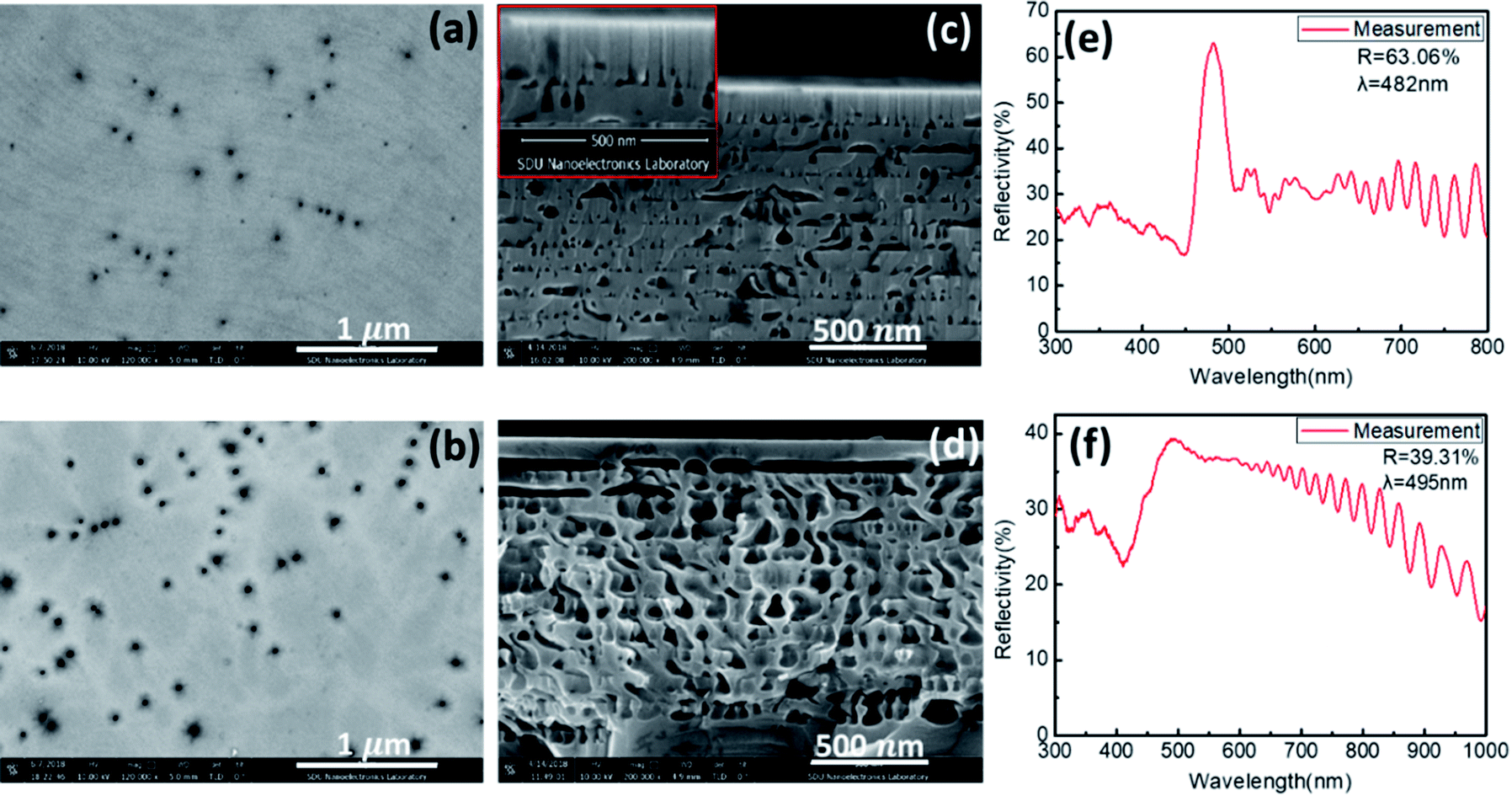 | ||
| Fig. 2 Top view (a) and (b) and cross-sectional (c) and (d) view SEM images and the corresponding reflectance spectra (e) and (f) of GaN nanostructured DBR produced by electrochemical etching in 0.3 M oxalic acid electrolyte at different biases of 12 V (a, c and e) and 18 V (b, d and f), respectively. | ||
By comparison, Fig. 3 shows the top view (a) and (b) and cross-sectional (c) and (d) view SEM images and the corresponding reflectance spectra (e) and (f) of nanostructured GaN-based DBR produced by electrochemical etching in 0.3 M NaNO3 electrolyte at different biases of 12 V (a, c and e) and 18 V (b, d and f), respectively. From the top view SEM images of nanostructured GaN DBR, as shown in Fig. 3(a) and (b), we can see some much smaller nanoscale pores formed on the sample surface, whose pore size is about 10–20 nm in diameter and almost remains constant with an increase in the applied bias; the pore density also increases from 4.3 × 108 cm−2 to 7.2 × 108 cm−2 with an increase in the applied bias. The pore size and porosity of porous GaN are the functions of applied etching bias and Si-doping concentration of the GaN layer, and increase on increasing either/both GaN layer doping concentration or/and applied etching bias.18,19 The pore size of porous GaN is in the range of 10–100 nm regardless of the GaN layer doping concentration and the applied etching bias. Therefore, we believe that there are no pores with diameter less than 10 nm formed in the n-GaN layers. The porosity of the formed porous GaN is low for low Si-doping GaN layer and high for high Si-doping GaN layer at fixed applied etching bias in the porous etching regime of the phase diagram for GaN EC etching.18 From the cross-sectional view SEM images of the samples, as shown in Fig. 3(c) and (d), triangular and elongated pores were formed in the n+-GaN layers; only a few nanopores were observed in the n−-GaN layer. The small pores and defects in n−-GaN layers would be the vertical porosification routes for the bottom n+-GaN layers.24 A clear interface between the n+-GaN layer and the n−-GaN layer was observed for both low and high applied bias conditions, indicating that good selectivity between the n+-GaN and n−-GaN layers can be achieved in NaNO3 electrolyte. The ratio of the elongated pores to the triangular pores of the samples increases with an increase in the applied bias because lateral etching was enhanced in the highly conductive n+-GaN layer. The measured and simulated reflectance spectra of the samples are shown in Fig. 3(e) and (f), and the measured reflectivity of the samples was 74.44% at 12 V and 86.39% at 18 V, respectively. The stopband width of the samples was 47 nm at 12 V and 67 nm at 18 V. The peak reflectivity wavelength of the samples shifted to shorter wavelength from 490 nm to 473 nm because of the increase in porosity of the nanostructured n+-GaN layer. The refractive index of the nanostructured GaN layer changed from 1.953 at 12 V to 1.926 at 18 V, which was obtained through the TMM simulation by taking 2.5 as the n−-GaN refractive index. As we can see, a higher applied bias resulted in a smaller refractive index of the nanostructured GaN, leading to a smaller optical thickness of the nanostructured GaN, which made the blue-shifted the central reflective wavelength. All the results imply that the samples had a better optical performance and NaNO3 electrolyte is a good electrolyte for making nanostructured GaN-based DBRs by electrochemical etching.
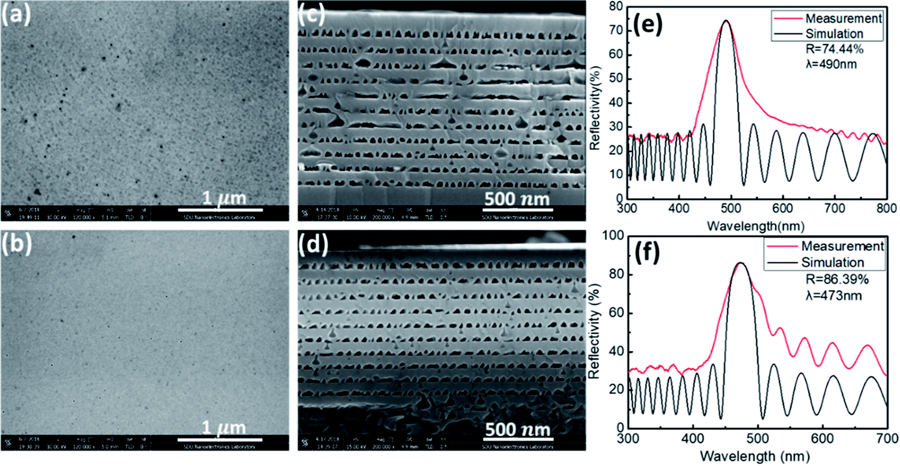 | ||
| Fig. 3 Top view (a) and (b) and cross-sectional (c) and (d) view SEM images and the corresponding reflectance spectra (e) and (f) of GaN nanostructured DBR produced by electrochemical etching in 0.3 M NaNO3 electrolyte at different biases of 12 V (a, c and e) and 18 V (b, d and f), respectively. | ||
To answer the question as to why the performance of nanostructured GaN-based DBR produced by using 0.3 M NaNO3 electrolyte is better than that produced by using 0.3 M oxalic acid electrolyte, the principal mechanism of porous GaN by EC process must be considered. It has been reported30 that porous GaN formation involves several stages during the EC process: (i) hole generation in GaN near the inside surface, (ii) GaN surface specific spot oxidation through hole transfer and recombination, and (iii) eventual dissolution of the oxidation complex in the electrolyte. The whole process includes potential distribution, ion drifting, mass transfer, and electrolyte flow and is very complex, which involves multifield dynamic theories in physics, chemistry, and nanofluidics.31 In our experiments, the GaN carrier concentration, applied bias, and electrolyte play a key role in the process. On comparing the EC conditions, the only difference is the ions in the electrolyte, which are Na+ and NO3− in NaNO3 and (C2O4)2− and H+ in oxalic acid. The most accepted reaction mechanism that the applied bias drove the generated holes in GaN to the surface resulted in the oxidation of the GaN surface has been proposed. Meanwhile, Ga3+ ions and N2 gas were generated near the GaN surface; thus, the nanostructured nanoporous GaN could be achieved.32 Based on some reports,13,33 the process can be express as:
| 2GaN + 6h+ + 3(C2O4)2− = Ga2(C2O4)3 + N2 in OA electrolyte | (1) |
| GaN + 3h+ +3NO3− = Ga(NO3)3 + ½N2 in NaNO3 electrolyte | (2) |
For eqn (1) and (2), both Ga2(C2O4)3 and Ga(NO3)3 are water soluble and easy to dissolve in the aqueous electrolyte. From the above analysis, we can predict that the different properties of nanostructured GaN-based DBR are attributed to different anions in the electrolytes because the only difference is the ions in the electrolyte in the whole process, as mentioned above. It may be due to (C2O4)2− being larger than NO3− in volume and more difficult to sink to the bottom of the pores during the process, leading to the random nanostructured porous GaN in Fig. 2(c) and (d). On the other hand, NO3− can go through the nanoscale channel easily and reach the bottom of the pore to continue the etching of the pores. Therefore, a uniform nanostructured GaN layer can be formed in NaNO3 electrolyte. We could estimate that (i) the performance of the nanostructured GaN-based DBR could be improved by tuning the EC etching condition and the thickness of the nanostructured GaN-based DBR alternative layer (n+-GaN and n−-GaN layer thickness); (ii) the other salt trinitrate, such as KNO3,33 also can be used as an electrolyte to produce uniform nanostructured GaN-based DBR.
The uniformity of DBR is an important property for real applications. To verify the uniformity of the nanostructured GaN-based DBR, we performed 2 inch wafer scale nanostructured GaN-based DBR in 0.3 M NaNO3 by EC at 18 V. Fig. 4(a) shows a photograph of the wafer-scale nanostructured GaN-based DBR under room-light illumination and the reflection of a business card with a Shandong University logo. The clear reflective images of the Shandong University logo were observed in the DBR region, indicating the high reflectivity of DBR. However, the unetched region is transparent and there is no observation of a reflective image of the Shandong University logo in the unetched region. The high reflection in the DBR region demonstrates the uniformity of the EC process. In order to further confirm the uniformity of the DBR, the reflectivity of the sample shown in Fig. 4(a) was measured on 5 labelled spots over the whole wafer and the unetched region (GaN sample before etching), as shown in Fig. 4(b). The detailed uniformity analysis is listed in Table 1. As can be seen, the reflectivity of the unetched region is ∼20%. On the other hand, the average reflectivity of DBR is about 83% with a small variation of 1.6%, which is consistent with the results shown in Fig. 3. The stopband width of the DBR is up to 80 nm with a negligible average variation of 0.02 nm over the 2 inch wafer scale. These results strongly confirmed the highly uniform DBR and the stable fabrication process.
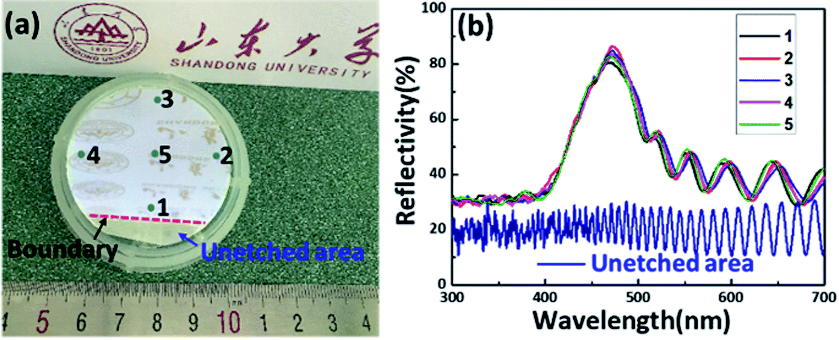 | ||
| Fig. 4 In wafer uniformity of the nanostructured GaN-based DBR. The optical image (a) and the measured reflectivity spectra (b) of the fabricated 2 inch scale nanostructured GaN-based DBR. | ||
![[R with combining macron]](https://www.rsc.org/images/entities/i_char_0052_0304.gif)
3.2 Performance tuning of the nanostructured GaN-based DBR
Based on the comparison of the results for nanostructured GaN DBR fabricated in different electrolytes, the better results of nanostructured GaN DBR can be obtained by using 0.3 M NaNO3 electrolyte in the electrochemical etching process. The nanostructured GaN-based DBR process was further optimized in 0.3 M NaNO3 electrolyte by tuning the EC applied bias to higher voltage (22 V) to achieve a uniform GaN nanostructure and high reflectivity of the nanostructured GaN DBR. The results are shown in Fig. 5. Fig. 5(a) shows the top view SEM image of the DBR and a similar morphology of the DBR was observed with Fig. 3(a) and (b), which has some nanoscale pores on the surface that serve as the etching starting points. Fig. 5(b) shows the cross-sectional SEM image of the DBR. A uniform porous GaN layer and a GaN layer alternative stack was formed, resulting in the high reflectivity of the nanostructured GaN-based DBR, as shown in Fig. 5(c). The reflectivity and stopband width of the DBR were measured to be 93.7% and 80 nm with the central wavelength of about 467 nm, respectively. The simulated reflectivity, central wavelength, and stopband width were matched with the measured results by taking 1.844 as the refractive index of the porous GaN layer.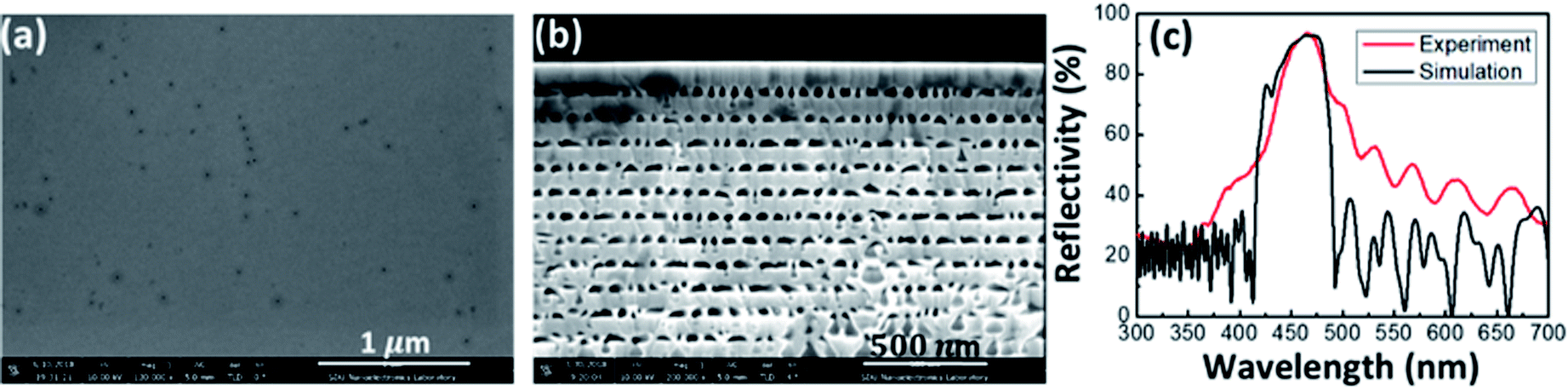 | ||
| Fig. 5 Top view (a) and cross-sectional view (b) SEM images and the experimental and simulated reflectance spectra (c) of GaN nanostructured DBR produced by EC etching in 0.3 M NaNO3 electrolyte at 22 V. | ||
Simulation is a powerful tool to study the properties of the DBR within a short time and low cost. By taking the advantages of the simulation, the properties of the nanostructured GaN-based DBR were analyzed by varying the thickness of the DBR alternative layer with other parameters fixed using Essential Macleod package based on the experimental results. The basic parameters of the DBR used in the simulation are listed in the Table 2. It is important to note that the refractive index of bulk GaN (n = 2.5) is used for alternate n−-GaN layers in the simulation, assuming that the small pores in these layers would not influence its properties. We fixed all the parameters of the nanostructured GaN-based DBR except the alternative layer thickness to study its performance. Fig. 6(a) shows the reflectivity of the DBR with different n−-GaN layer thickness in the range from 57 nm to 107 nm based on the fabricated DBR n−-GaN layer thickness listed in Table 2. Fig. 6(b) shows the reflectivity of the DBR with different nanostructured GaN layer thickness in the range from 27 nm to 77 nm based on the fabricated DBR n+-GaN layer thickness listed in Table 2. Fig. 6(c) shows the reflectivity of the DBR with tuning of the nanostructured GaN layer from 27 nm to 77 nm and the n−-GaN layer thickness from 57 nm to 107 nm. It can be seen that: (i) the peak reflective wavelength of the DBR shifted to longer wavelength from near UV to near IR with an increase in the thickness of the DBR alternative layers because of n1t1 = n2t2 = λ/4; the thicker alternative layer resulted in longer peak wavelength, as shown in Fig. 6(d). (ii) The stopband width of the DBR became wider with an increase in the thickness of the alternative layer, which could be due to the more uniform porous nanostructure formed in the DBR. Up to 200 nm stopband width can be achieved by increasing the period layer thickness (as shown in Fig. 6(e)). (iii) The reflectivity of the DBR also increased gradually and reached near 100% on increasing the period layer thickness, as shown in Fig. 6(f).
| Al2O3 substrate | GaN buffer layer | n+-GaN layer (nanostructured layer) | n−-GaN layer | |
|---|---|---|---|---|
| Thickness (nm) | — | 3000 | 37 | 67 |
| Refractive index (n) | 1.67 | 2.5 | 1.844 | 2.5 |
| Doping concentration (1 × 1018 cm−3) | — | — | 10 | 2 |
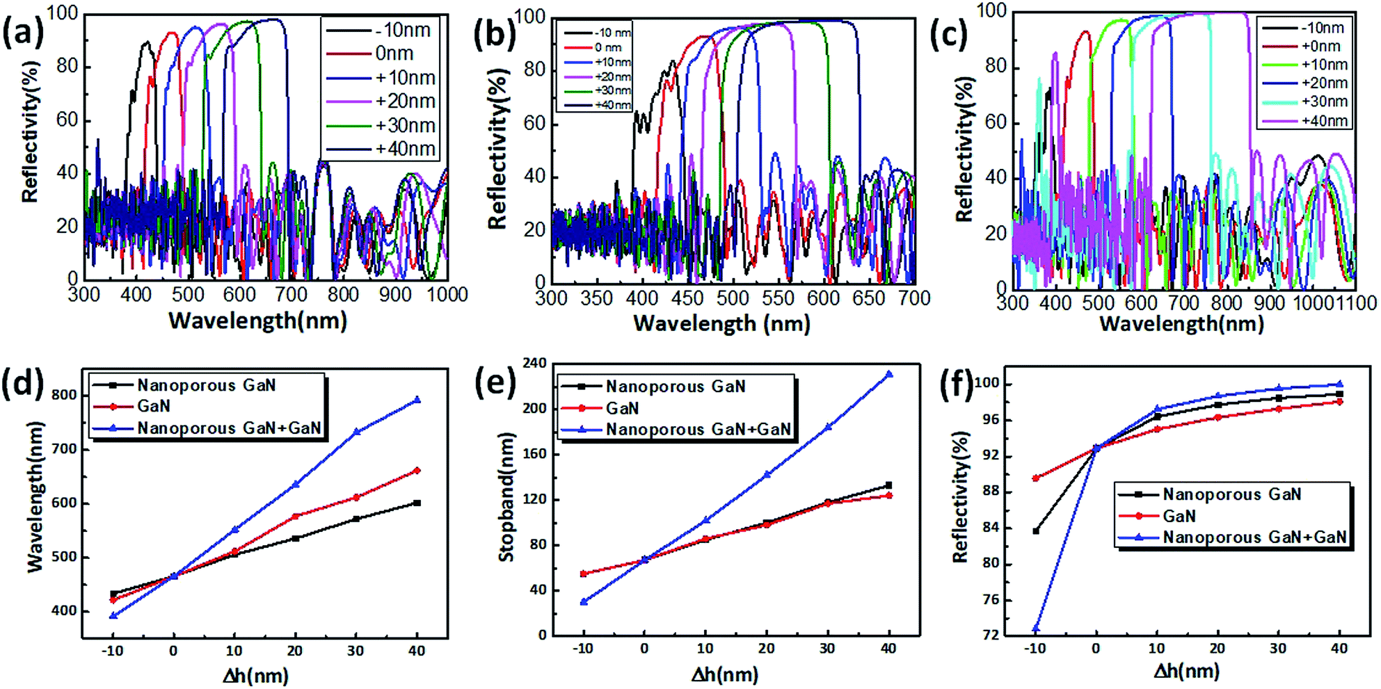 | ||
| Fig. 6 Simulated reflectance spectra of nanostructured GaN-based DBR by tuning the (a) GaN layer thickness, (b) porous GaN layer thickness, and (c) both of the GaN and porous GaN layer thickness. (d) Central wavelength, (e) stopband width, and (f) reflectivity of the nanostructured GaN-based DBR as a function of the thickness of DBR alternative layers. | ||
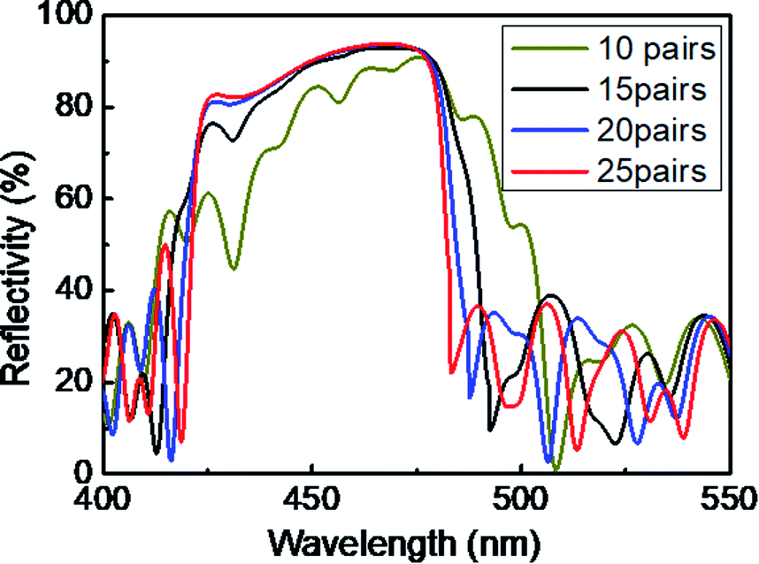
The pair number of the DBR is another key parameter influencing the real applications. Fig. 7 shows the simulated reflective spectra of the nanostructured GaN-based DBR with a variation in the alternative layer pairs from 10 to 25. It can be seen that the reflectivity of the DBR does not always increase with the increase in the number of alternating layer pairs in the nanostructured GaN-based DBR. Only a little improvement in the reflectivity is observed on increasing the DBR pairs from 15 to 20 and almost the same reflectivity value is obtained on increasing the DBR pairs from 20 to 25. But the reflectivity of the DBR drops quickly when the DBR pairs reduce from 15 to 10. This could be due to the fact that there will be more scattering effect at the roughening interfaces in the porous layers of the DBR nanostructure.34 The results implied that there is a minimum alternative period pair for maximum reflectivity of the nanostructured GaN-based DBR with certain alternative layer thickness. The reflectivity of the nanostructured GaN-based DBR would not increase on increasing the alternative pair after the DBR reached certain pairs. We have to tune the other parameter, for instance, the alternative layer thickness and the applied bias, to reach higher reflectivity (near 100%). It should be noted that nearly 100% reflectivity of the nanostructured GaN-based DBR with 15 period pairs could be achieved by tuning the period thickness and the applied bias, which provided the DBR design and application flexibility.
 | ||
| Fig. 7 Simulation reflectivity spectra of the nanostructured GaN-based DBR with different pairs. | ||
3.3 Nanostructured GaN DBR for optoelectronic device application
To demonstrate the optoelectronic applications, the GaN-based LEDs with nanostructured GaN-based DBR were fabricated and characterized. Fig. 8(a) shows the wafer-level real lit-up blue LED with nanostructured GaN-based DBR on the testing probe station and the inset shows the optical microscope images of the processed micro-LED. Fig. 8(b) shows the cross-sectional SEM image of the LED sample with nanostructured GaN-based DBR. The clear nanostructured GaN-based DBR is formed under InGaN/GaN MQWs after the EC process in 0.3 M NaNO3 electrolyte at 18 V without any degradation of the InGaN/GaN MQWs active layer. The room-temperature PL curves of the LEDs without and with nanostructured GaN-based DBR produced in 0.3 M NaNO3 electrolyte at 18 V were obtained to explore the influence of the DBR layer on the LED optical properties, as shown in Fig. 8(c). All the LED samples emit at a wavelength of about 460 nm. A 6 times enhanced PL peak intensity can be observed for the LED with nanostructured GaN-based DBR. This is because the formed nanostructured GaN-based DBR can effectively increase light scattering, resulting in better light extraction.35 The L–I–V characteristics of unpackaged LEDs from the LEDs with and without nanostructured GaN-based DBR are shown in Fig. 8(d) and the inset shows the optical microscope image of the lit-up LED with nanostructured GaN-based DBR. Under a driving current of 20 mA, the forward voltages of the LEDs with and without nanostructured GaN-based DBR were 3.5 V and 3.4 V, respectively. The output power of the LEDs with and without nanostructured GaN-based DBR was measured to be 4.7 mW and 3.1 mW, respectively. The light output power improvement of about 150% was obtained. Therefore, it can be concluded that the LED performance is enhanced as the light extraction is improved by the nanostructured GaN-based DBR layer.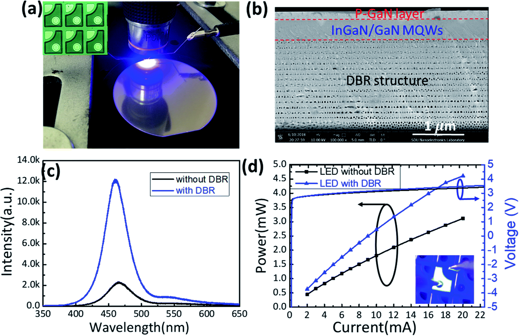 | ||
| Fig. 8 (a) Real lit-up blue LED with GaN nanostructured DBR on a 2 inch wafer, (b) the cross-sectional SEM image of the LED, (c) PL spectra and (d) L–I–V of LED with (blue line) and without (black line) nanostructured GaN-based DBR (inset: optical images of the LED). | ||
4. Conclusions
In summary, the nanostructured GaN-based DBR was fabricated by using all Si-doped GaN layers and was optimized both experimentally and simulatively using electrochemical etching in different electrolytes and TMM method. High performance nanostructured GaN based DBR with high reflectivity (>93%) and broad stopband (∼80 nm) was achieved in neutral sodium nitrate by EC, and nanostructured GaN DBR with nearly 100% reflectivity and full visible spectrum range can be designed by tuning the thickness of the alternative layers of nanostructured GaN DBR. The photoluminescence (PL) and light-out power enhancements of the GaN-based micro-LED are 6 times and 150% without the degradation of electrical performance, respectively, which was achieved by the incorporation of the fabricated nanostructured GaN-based DBR in the micro-LED that contributes to the strong light scattering from the DBR layer. We believe that this work will pave a way to high performance GaN-based optoelectronics devices and guide the applications in the field of flexible devices and biomedical sensors.Conflicts of interest
The authors declare no conflict of interest.Acknowledgements
This research was funded by the Key Research Plan of Shandong Province (2017GGX10106), Natural Science Foundation for Distinguished Young Scientist of Shandong Province (JQ201814), and the Fundamental Research Funds of Shandong University (2017TB0020); Collaborative Innovation Center of Technology and Equipment for Biological Diagnosis and Therapy in Universities of Shandong. We would like to thank Haiyan Yu, Xiaomin Zhao, Sen Wang, and Yuyu Guo from the State Key laboratory of Microbial Technology of Shandong University for help and guidance in material characterization.Notes and references
- J. Cho, J. H. Park, J. K. Kim and E. F. Schubert, Laser Photonics Rev., 2017, 11, 1600147 CrossRef.
- T. J. Slight, S. Watson, S. Viola, A. Yadav, S. Stanczyk, S. Grzanka, S. Gwyn, E. Rafailov, P. Perlin, S. P. Najda, M. Leszczynski, M. Haji and A. E. Kelly, in Novel In-Plane Semiconductor Lasers Xviii, ed. A. A. Belyanin and P. M. Smowton, 2019, p. 10939 Search PubMed.
- H. Amano, Y. Baines, E. Beam, M. Borga, T. Bouchet, P. R. Chalker, M. Charles, K. J. Chen, N. Chowdhury, R. Chu, C. De Santi, M. M. De Souza, S. Decoutere, L. Di Cioccio, B. Eckardt, T. Egawa, P. Fay, J. J. Freedsman, L. Guido, O. Haeberlen, G. Haynes, T. Heckel, D. Hemakumara, P. Houston, J. Hu, M. Hua, Q. Huang, A. Huang, S. Jiang, H. Kawai, D. Kinzer, M. Kuball, A. Kumar, K. B. Lee, X. Li, D. Marcon, M. Maerz, R. McCarthy, G. Meneghesso, M. Meneghini, E. Morvan, A. Nakajima, E. M. S. Narayanan, S. Oliver, T. Palacios, D. Piedra, M. Plissonnier, R. Reddy, M. Sun, I. Thayne, A. Torres, N. Trivellin, V. Unni, M. J. Uren, M. Van Hove, D. J. Wallis, J. Wang, J. Xie, S. Yagi, S. Yang, C. Youtsey, R. Yu, E. Zanoni, S. Zeltner and Y. Zhang, J. Phys. D: Appl. Phys., 2018, 51, 163001 CrossRef.
- S. Nakamura, T. Mukai and M. Senoh, Jpn. J. Appl. Phys., 1991, 30, L1998–L2001 CrossRef CAS.
- M. Weis, C. Friesicke, R. Quay and O. Ambacher, 2018 IEEE MTT-S International Microwave Workshop Series on 5G Hardware and System Technologies, IMWS-5G, Dublin, Ireland, Aug. 2018, pp. 30–31 Search PubMed.
- F. Wang and L. Bo, Gallium Nitride-enabled High Frequency and High Efficiency Power Conversion. Integrated Circuits and Systems, ed. G. Meneghesso, M. Meneghini and E. Zanoni, Springer, Cham, 2018, pp. 153–180 Search PubMed.
- H. C. Yu, Z. W. Zheng, Y. Mei, R. B. Xu, J. P. Liu, H. Yang, B.-p. Zhang, T. C. Lu and H. C. Kuo, Prog. Quantum Electron., 2018, 57, 1–19 CrossRef.
- Z. Wu, X. Zhang, A. Fan, H. Chen, J. Zhao, S. Chen, S. Wang and Y. Cui, Mater. Lett., 2019, 235, 116–119 CrossRef CAS.
- C. Berger, A. Dadgar, J. Bläsing, A. Lesnik, P. Veit, G. Schmidt, T. Hempel, J. Christen, A. Krost and A. Strittmatter, J. Cryst. Growth, 2015, 414, 105–109 CrossRef CAS.
- D. Chen, H. Xiao and J. Han, J. Appl. Phys., 2012, 112, 064303 CrossRef.
- T. Mitsunari, T. Tanikawa, Y. Honda, M. Yamaguchi and H. Amano, J. Cryst. Growth, 2013, 370, 16–21 CrossRef CAS.
- Y. Zhang, S.-W. Ryu, C. Yerino, B. Leung, Q. Sun, Q. Song, H. Cao and J. Han, Phys. Status Solidi B, 2010, 247, 1713–1716 CrossRef CAS.
- F. Hou, M.-R. Zhang, Q.-M. Jiang, Z.-G. Wang, J.-H. Yan and G.-B. Pan, Mater. Lett., 2018, 223, 194–197 CrossRef CAS.
- Z. Yu, B. Leung and J. Han, Appl. Phys. Lett., 2012, 100, 181908 CrossRef.
- Y. Zhang, Q. Sun, B. Leung, J. Simon, M. L. Lee and J. Han, Nanotechnology, 2011, 22, 045603 CrossRef PubMed.
- S.-W. Ryu, Y. Zhang, B. Leung, C. Yerino and J. Han, Semicond. Sci. Technol., 2012, 27, 015014 CrossRef.
- A. Ramizy, Z. Hassan and K. Omar, Sens. Actuators, B, 2011, 155, 699–708 CrossRef CAS.
- L. Han, J. Zhou, Y. Sun, Y. Zhang, J. Han, J. Fu and R. Fan, J. Nanotechnol. Eng. Med., 2014, 5, 0410041–0410049 Search PubMed.
- C. Zhang, S. H. Park, D. Chen, D.-W. Lin, W. Xiong, H.-C. Kuo, C.-F. Lin, H. Cao and J. Han, ACS Photonics, 2015, 2, 980–986 CrossRef CAS.
- G. Y. Shiu, K. T. Chen, F. H. Fan, K. P. Huang, W. J. Hsu, J. J. Dai, C. F. Lai and C. F. Lin, Sci. Rep., 2016, 6, 8 CrossRef PubMed.
- G. Yuan, C. Zhang, K. Xiong and J. Han, Opt. Lett., 2018, 43, 5567–5570 CrossRef CAS PubMed.
- J. Park, J.-H. Kang and S.-W. Ryu, Appl. Phys. Express, 2013, 6, 072201 CrossRef.
- D. Cao, X. Yang, L. Shen, C. Zhao, C. Luan, J. Ma and H. Xiao, Photon. Res., 2018, 6, 1144–1150 CrossRef CAS.
- T. Zhu, Y. Liu, T. Ding, W. Y. Fu, J. Jarman, C. X. Ren, R. V. Kumar and R. A. Oliver, Sci. Rep., 2017, 7, 45344 CrossRef CAS PubMed.
- F.-H. Fan, Z.-Y. Syu, C.-J. Wu, Z.-J. Yang, B.-S. Huang, G.-J. Wang, Y.-S. Lin, H. Chen, C. H. Kao and C.-F. Lin, Sci. Rep., 2017, 7, 4968 CrossRef PubMed.
- D. Chen and J. Han, Appl. Phys. Lett., 2012, 101, 221104 CrossRef.
- S.-M. Lee, J.-H. Kang, J. K. Lee and S.-W. Ryu, Electron. Mater. Lett., 2016, 12, 673–678 CrossRef CAS.
- K. Al-Heuseen, M. R. Hashim and N. K. Ali, Appl. Surf. Sci., 2011, 257, 6197–6201 CrossRef CAS.
- F. C. P. Massabuau, P. H. Griffin, H. P. Springbett, Y. Liu, R. V. Kumar, T. Zhu and R. A. Oliver, APL Mater., 2020, 8, 031115 CrossRef.
- L. Tommasino, G. Zapparoli and R. V. Griffith, Nucl. Tracks, 1980, 4, 191–196 CrossRef CAS.
- S. L. Guo, B. L. Chen and S. A. Durrani, Handbook of Radioactivity Analysis, 2012, vol. 82, pp. 233–298 Search PubMed.
- C. Youtsey, I. Adesida and G. Bulman, Appl. Phys. Lett., 1997, 71, 2151–2153 CrossRef CAS.
- C. Zhang, G. Yuan, A. Bruch, K. Xiong, H. X. Tang and J. Han, J. Electrochem. Soc., 2018, 165, E513–E520 CrossRef CAS.
- J. Volk, K. Ferencz, J. J. Ramsden, A. L. Toth and I. Barsony, Phys. Status Solidi A, 2005, 202, 1703–1706 CrossRef CAS.
- X. Lu, J. Li, K. Su, C. Ge, Z. Li, T. Zhan, G. Wang and J. Li, Nanomaterials, 2019, 9, 862 CrossRef CAS PubMed.
Footnote |
| † Bin Wei and Yingkuan Han contributed equally |
| This journal is © The Royal Society of Chemistry 2020 |