
 Open Access Article
 This Open Access Article is licensed under a Creative Commons Attribution-Non Commercial 3.0 Unported Licence
Strongly enhanced efficiency of polymer solar cells through unzipped SWNT hybridization in the hole transport layer
Wenna Zhang†
a,
Fanchen Bu†a,
Wenfei Shen a,
Xiaohua Qia,
Na Yanga,
Mengyao Chena,
Di Yanga,
Yao Wanga,
Miaorong Zhanga,
Haoyang Jianga,
Peter Strizhak*b and
Jianguo Tang*a
a,
Xiaohua Qia,
Na Yanga,
Mengyao Chena,
Di Yanga,
Yao Wanga,
Miaorong Zhanga,
Haoyang Jianga,
Peter Strizhak*b and
Jianguo Tang*a
aInstitute of Hybrid Materials, National Center of International Joint Research for Hybrid Materials Technology, National Base of International Sci. & Tech. Cooperation on Hybrid Materials, Qingdao University, 308 Ningxia Road, Qingdao 266071, P. R. China. E-mail: jianguotangde@hotmail.com
bL.V. Pysarzhevsky Institute of Physical Chemistry, National Academy of Sciences of Ukraine, Ukrainian Academy of Sciences, 31 prosp. Nauky, Kyiv 03028, Ukraine. E-mail: pstrizhak@hotmail.com
First published on 2nd July 2020
Abstract
Single-walled carbon nanotubes (SWNTs) have good conductivity, but their size can't match the heterojunction nanostructure in polymer solar cells (PSCs). To improve the photovoltaic performance of PSCs, herein, a faciley fabricated composite hole transport layer composed of unzipped single-walled carbon nanotubes (uSWNTs) and poly(3,4-ethylenedioxythiophene):polystyrene sulfonate (PEDOT:PSS) is effectively applied for PSC devices. Compared with the pure PEDOT:PSS hole transport layer (HTL) without uSWNTs, the uSWNTs/PEDOT:PSS layer shows more effective performance as the hole transportation layer. Optimizing the uSWNT concentration in PEDOT:PSS results in fabrication of the PSC devices with uSWNTs/PEDOT:PSS hole transport layers that exhibit greatly improved average power conversion efficiency (PCE), from 13.72% to 14.60%, and greatly enhanced current density and fill factor, which can be ascribed to the increased conductivity and hole transport efficiency. Our approach also supports simple solution-processing techniques and the insensitivity of the performance to thickness, which promises that the faciley fabricated uSWNTs/PEDOT:PSS layer has more potential to be applicable to the roll-to-roll process of PSC fabrication with extremely low cost.
1. Introduction
Polymer solar cells (PSCs) have attracted enormous attention as a potential cheap renewable energy source with the possibilities of high output and potential large-scale production.1,2 Recently, PSCs have achieved significant improvements in power conversion efficiency (PCE) owing to new high-performance materials.3 However, designing advanced device structures and optimizing the fabrication techniques are the ongoing topics to improve the performances of PSCs in which the hole transportation layer (HTL) is one key aspect due to its designable characteristics.4 Currently, poly(3,4-ethylenedioxythiophene)-doped poly(styrene sulfonate) (PEDOT:PSS) is a widely used HTL. Typically, the layer thickness is about 40 nm which limits further modification of the HTL.5,6 Therefore, a new way is needed to dope the HTL structure and develop new technology for low-cost solution-processing.7–9 From this point of view, the hybrid strategy of PEDOT:PSS with dopants is one of the worthy choices due to its simplicity and validity.As a potential nano-dopant candidate, carbon nanotube (CNT) is a linear nanomaterial10,11 which has been commercialized with the trend of cost decrease based on the large-scale synthetic technology development. The CNT applications have distributed in wide fields, e.g., energy storage/conversion, electronic devices, and sensors.12 However, CNT can't be applied directly for PSCs as a dopant because the CNT linear size is too long (more than 5 μm) to match the PSC layer structure. This makes us think about the possibility to re-structure pristine CNTs into the available dopant.13 In the two main types of single-walled (SWNTs) and multi-walled (MWNTs), SWNTs can be seen as a roll of a single layer of graphene, and MWNTs can be regarded as a roll of multi-layers of graphene sheets.11,14 Therefore, the unzipped CNTs can be considered as the combinations of residue CNTs and generated graphene. These rich structural species have similar properties with curved graphene sheets.15–18 However, the structural advantage of unzipped CNTs concerns the inherited linear geometry, not 2-D fragments. Moreover, the size-controllable advantage of unzipped CNTs is more applicable in concise structure devices.19
In recent years, the heuristic researches are of graphene applications for dye-sensitized solar cells and planar heterojunction perovskite solar cells to enhance the efficiencies of the related devices.4,19–21 A novel work on pristine CNTs used as a hybrid hole collector for inverted planar perovskite solar cells was reported.22–24 These studies show the effectiveness of nanocarbon materials to improve efficiencies of photovoltaic devices.
The heterostructure junction (HSJ) in PSCs makes the initial difference between perovskite and polymer solar cells.4,7,25 Mixing initial SWNTs with PEDOT:PSS as HTL on PSCs decomposes the two-phase nano-structures of PSCs due to large size and poor dispersion of pristine SWNTs. Moreover, the random packing of SWNTs may form voids, which will inhibit the electron/hole transportations and further reduce device efficiency.22,26–28 Hopefully, using uSWNTs can avoid these problems which arise from pristine SWNTs because uSWNTs have a decreased size and increased surface area that may generate ideal compatibility and high conductivity for transporting electrons and holes.
In this work, we demonstrated a facile method to fabricate an effective hole transport layer of uSWNTs/PEDOT:PSS to enhance the photovoltaic performances of polymer solar cells. The PSCs with uSWNTs-doped PEDOT:PSS layer exhibits high power conversion efficiency (PCE), which indicating the mixed structure of uSWNTs/PEDOT:PSS improves the conductivity and improves the charge transfer characteristics. Therefore, our study shows that uSWNTs/PEDOT:PSS nanocomposites can be used as HTLs for high-performance PSCs.
2. Experimental
2.1. Materials
To fabricate PSCs, the photoactive materials PFN and IT-4F were purchased from Solarmer Materials Inc. (Beijing, China). Poly(3,4-ethylenedioxythiophene)–polystyrene sulfonate (PEDOT:PSS, Al 4083) was obtained from Bayer, Germany. Patterned ITO (indium tin oxide) glass substrates with a sheet resistance of 15 Ω sq−1 were purchased from Shenzhen Display (Shenzhen, China). Single-walled carbon nanotubes were purchased from Xianfeng Nanomaterials Technology Co., Ltd. Potassium permanganate, sulfuric acid, hydrochloric acid, and hydrogen peroxide were purchased from Beijing National Pharmaceutical Group Chemical Reagent Co., Ltd. All reagents were used without further purification.2.2. Synthesis of uSWNTs and uMWNTs
The preparation of the uSWNTs or uMWNTs was performed following the modified Hummers' method.29 Accordingly, 0.2 g of SWNTs or MWNTs were suspended in 35 mL of concentrated sulfuric acid and then stirred at 1000 rpm for 10 h using a magnetic stirrer until a visually homogeneous black solution formed. Then, 1 g of KMnO4 with five portions 0.2 g each was added slowly to the solution and further stirred for 1 h at room temperature. After that, the temperature was gradually raised to 50 °C and maintained at that temperature for 2 h in a water bath. When the reaction was complete, the product was purified and dried with a series of steps. Briefly, the solution was removed from the heat source and cooled in the ice bath, cooled to room temperature, and poured into 350 g of ice containing 5 mL of 30% H2O2. Then, a proper amount of H2O2 (30%) was added drop by drop until no gas was observed (to prevent precipitation of insoluble MnO2). The mixtures were then centrifuged (10![[thin space (1/6-em)]](https://www.rsc.org/images/entities/char_2009.gif) 000 rpm, 30 min) to give crude uSWNTs and uMWNTs solid. The product was washed by centrifugation with hydrochloric acid (the ratio of DI water to hydrochloric acid is 3:1) and deionized water. The clean precipitate was redistributed in deionized water by sonication and centrifuged to remove coarse particles and unreacted SWNTs or MWNTs, and dried in a vacuum oven at 80 °C overnight. The purified uSWNTs and uMWNTs were collected. The detailed preparation process is schematically depicted in Fig. 1(c).
000 rpm, 30 min) to give crude uSWNTs and uMWNTs solid. The product was washed by centrifugation with hydrochloric acid (the ratio of DI water to hydrochloric acid is 3:1) and deionized water. The clean precipitate was redistributed in deionized water by sonication and centrifuged to remove coarse particles and unreacted SWNTs or MWNTs, and dried in a vacuum oven at 80 °C overnight. The purified uSWNTs and uMWNTs were collected. The detailed preparation process is schematically depicted in Fig. 1(c).
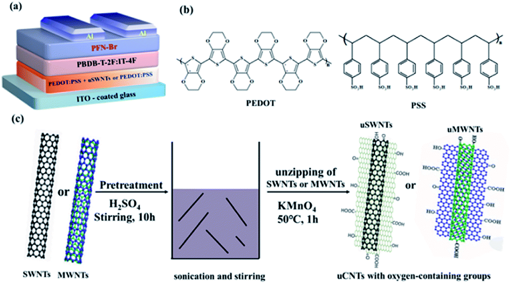 | ||
| Fig. 1 (a) Schematic illustration of the device architecture used in this work. (b) The molecular structure of PEDOT and PSS. (c) Schematic of uSWNTs or uMWNTs synthesis. | ||
2.3. Device fabrication
The device structure of PSCs (Fig. 1) is characterized by the following layers fabrication, glass/ITO/uSWNTs/PEDOT:PSS/PBDB-T-2F:IT-4F/PFN-Br/Al. Hybrid PEDOT:PSS composites doped with uSWNTs were prepared by a facile solution processing method. The fixed volume ratio of uSWNTs/PEDOT:PSS was 7:3, and the variable amount was added with different concentrations of SWNTs. ITO substrates with the conductivity of 15 Ω sq−1 were ultrasonically cleaned for 15 min via ITO cleaning agent, deionized water, acetone, and isopropyl alcohol, respectively, followed by UV–ozone treatment for 5 min. The PEDOT:PSS is rotated onto the substrate at 4000 rpm for 20 s, and then annealed at 160 °C for 20 minutes in the air. The uSWNTs/PEDOT:PSS mixtures with various concentrations were spin-coated in the same way as the pure PEDOT:PSS to form an anode buffer layer. The ITO substrate with anode buffer layer was then transferred a nitrogen-filled glove box. The PBDB-T-2F–IT-4F solution was dissolved in chlorobenzene with 1.8-diiodooctane as an additive at 40 °C and stirred overnight. The PBDB-T-2F–IT-4F mixed solution was spin-coated on the anode buffer layer for 40 s, and then annealed at 100 °C for 10 minutes. Subsequently, PFN-Br was spin-coated on the active layer at 3000 rpm for 30 s, and then transferred to a vacuum chamber (<5 × 10⁻⁴ Pa) and 100 nm Al was vapor-deposited onto the active layer by thermal evaporation.
2.4. Characterization
A high-resolution transmission electron microscope (HRTEM) was performed using a FEI Talos F200i microscope (Thermo Fisher Scientific Inc.). Fourier transform infrared spectroscopy (FTIR) data were measured using a Nicolet 6700 Fourier transform infrared spectrometer from Thermo Corporation, Waltham, USA. Optical properties were characterized by a UV-visible spectrometer (Lambda 750S) with a wavelength range of 200 to 800 nm. X-ray diffraction (XRD) was performed by a Bruker D8 Advance model in a wide angular range (2θ = 10–80°) at a scan speed of 2° min−1 and has single-color CuKα radiation (k = 1.5406 Å). The Raman spectrometer was performed using an Almega Thermo Nicolet Dispersion Raman spectrometer. The specific surface area of the samples were explored via Automatic specific surface area (Tristar3000). X-ray photoelectron spectroscopy (XPS) data were measured using the ESCALAB250Xi electron spectrometer, and its radiation is 150 watts from Waltham, USA. Measured by Keithley 2420 light source (Shenzhen, China). For devices characterization, the optical transmittance of the hole-collecting film was measured using a UV-visible spectrophotometer (Lambda 750S). In a nitrogen-filled glove box, the current density–voltage (J–V) characteristics were recorded using a solar simulator under AM 1.5G solar lighting. The external quantum efficiencies (EQEs) of inverted PSCs were analysed using an incident photon conversion efficiency (IPCE) measurement system certified by Newport, USA.3. Results and discussion
Fig. 2 shows the TEM images of SWNTs, uSWNTs, MWNTs, and uMWNTs. Pristine SWNTs have a tubular structure (Fig. 2(a)). After acidic treatment (Fig. 2(b)), the tubular structure partially splits and the broken surface is generated. TEM image suggests that the surface of the SWNTs has wrinkles and the width becomes larger after unzipping which is caused by the strong oxidation process. Fig. 2(c) shows hollow tubular structures for pristine MWNTs. The lateral size of the corresponding carbon nanostructures becomes bigger after unzipping as it follows from a comparison of images presented in Fig. 2(c) and (d). Moreover, the generated fragments of graphene-like structures for several MWNTs are observed in Fig. 2(d). Increasing the lateral size may support enhance the efficiency of unzipped carbon nanotubes in PSCs.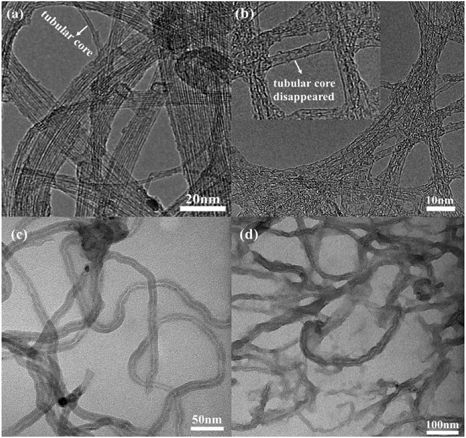 | ||
| Fig. 2 TEM images of (a) pristine SWNTs, (b) uSWNTs, (c) pristine MWNTs, and (d) uMWNTs. | ||
Fig. 3(a) gives FTIR spectra of SWNTs, MWMTs, uSWNTs, and uMWNTs. The broad peak at ca. 3400 cm−1 indicates the presence of –OH. A weak absorption band observed near 1730 cm−1 indicates the presence of the C![[double bond, length as m-dash]](https://www.rsc.org/images/entities/char_e001.gif) O tensile. The peaks near 1213 cm−1 and 1044 cm−1 observed for uSWNTs are related to the C–O asymmetric stretching. Comparison of SWNTs and uSWNTs indicates a slightly higher intensity of carboxylic and alkoxy groups and a very higher intensity of –OH group for unzipped CNTs. Probably, the oxidants may be mainly used to oxidize the already-formed functional groups.30 We observe a weaker intensity of the characteristic bands of functional oxygen groups on uMWNTs that may be an indication of the weaker unzipping and only partial oxidation of MWNTs. TEM and FTIR data suggest that the strong permanganate oxidation forms oxygen-containing groups that are the unzipped sp2-carbon product.11,30,31 Increasing the amount of the functional oxygen groups should help dispersion of unzipped CNTs in PSCs.
O tensile. The peaks near 1213 cm−1 and 1044 cm−1 observed for uSWNTs are related to the C–O asymmetric stretching. Comparison of SWNTs and uSWNTs indicates a slightly higher intensity of carboxylic and alkoxy groups and a very higher intensity of –OH group for unzipped CNTs. Probably, the oxidants may be mainly used to oxidize the already-formed functional groups.30 We observe a weaker intensity of the characteristic bands of functional oxygen groups on uMWNTs that may be an indication of the weaker unzipping and only partial oxidation of MWNTs. TEM and FTIR data suggest that the strong permanganate oxidation forms oxygen-containing groups that are the unzipped sp2-carbon product.11,30,31 Increasing the amount of the functional oxygen groups should help dispersion of unzipped CNTs in PSCs.
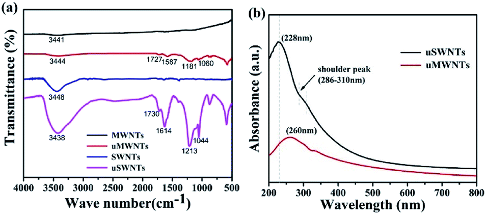 | ||
| Fig. 3 (a) FTIR spectrum of MWNTs, uMWNTs, SWNTs, and uSWNTs. (b) UV-vis absorption spectra of the uSWNTs and uMWNTs. | ||
UV-vis absorption spectra of the uSWNTs and uMWNTs are presented in Fig. 3(b), in which the photon absorption is a single strong peak for all samples. The appearance of the peak is due to the sp2 hybridization of the material and the linking units, e.g., CC, CO, and C–O bonds. The uSWNTs show a strong peak at 228 nm corresponds to π–π* transition of CC, and the shoulder peak from 286 to 310 nm which corresponds to n–π* transition of CO.32,33 The absorption of uMWNTs in the UV region is weaker compared to uSWNTs, a single strong peak at 260 nm is mainly related to CC, but the shoulder peaks are not obvious. Based on FTIR and UV-vis characterizations, the uSWNTs sample has a higher oxidation degree and may have better dispersion stability in PSCs compared to uMWNTs.
The XRD pattern reflects the typical structural characteristics of SWNTs and MWNTs as shown in Fig. 4(a) and (b). Due to the single structure of SWNTs, the XRD spectrum has broad peaks as it follows from the data presented in Fig. 4(a). After unzipping, the XRD pattern of uSWNTs sample becomes broader and flatter, suggesting that the initial cylinder structure was oxidized and unzipped, indicating more amorphous characteristics of uSWNTs. A strong peak at 26.1° is observed in Fig. 4(b), which is assigned to (002) diffraction of the graphitic layer-by-layer structure. After treating with the strong oxidant (sample uMWNTs), the intensity of the peak in 26.1° decreases, whereas a broad peak located at ∼25° appears, which reflects the change in the atomic arrangement of MWNTs due to the large number of oxygen-containing functional groups introduced into the graphite intermediate layer by the oxidation process.34,35 Therefore, the MWNTs have been successfully unzipped. We should point out that the lattice arrangement of the SWNTs and MWNTs carbon atoms is destroyed and the oxygen-containing groups increased after unzipping. These observations are in good agreement with TEM, FTIR, and UV-vis data.
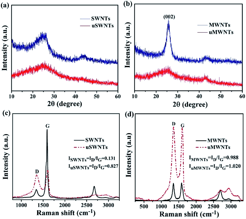 | ||
| Fig. 4 XRD spectra of (a) SWNTs and uSWNTs, (b) MWNTs and uMWNTs. Raman spectra of (c) SWNTs and uSWNTs, (d) MWNTs and uMWNTs. | ||
Fig. 4(c) and (d) shows the Raman spectra of the SWNTs, uSWNTs, MWNTs, and uMWNTs recorded with a 532 nm (2.34 eV) laser excitation wavelength. Pristine SWNTs show strong G-band at 1592 cm−1 and a very weak D-band, indicating that SWNTs are of high quality15 which is in a good agreement with TEM. After unzipping, a strong D-band (1261 cm−1) and a falling G-band (1604 cm−1) are observed. The significant increase in the intensity ratio (ID/IG) between D-band and G-band also confirms the unzipping of SWNTs. The decrease in G-band reflects that some carbon atoms have been removed and a large number of oxygen-containing functional groups has been introduced. A significant increase in D-band is attributed to carbon defects introduced at the edges and on the surface of uSWNTs.34 Fig. 4(d) shows that MWNTs and uMWNTs have G-band and D-band at similar positions. After unzipping, the intensity ratio (ID/IG) of D-band and G-band increases. It confirms that the intervention of a large number of oxygen-containing functional groups causes the damage of both, the graphite structure and the tubular structure. This observation is in good agreement with TEM and XRD data.
The specific surface area of samples were studied from the N2 adsorption–desorption isotherm. At standard temperature and pressure, the N2 adsorption–desorption isotherm for SWNTs, uSWNTs, MWNTs and uMWNTs are shown in Fig. 5. The values of BET specific surface area of pristine SWNTs was 495 m2 g−1, whereas the specific surface area of uSWNTs was 641 m2 g−1 in Fig. 5(a). Identically, specific surface area for pristine MWNTs was 143 m2 g−1, whereas the specific surface area of uMWNTs was 187 m2 g−1 in Fig. 5(b). The significant enhancement in the surface area of unzipped CNTs confirms that the small outer layer of the pristine CNTs has been successfully unraveled. It is observed that the unzipped CNTs has more nitrogen adsorption than the pristine CNTs, which means that the microporous surface area of the unzipped CNTs is enhanced owing to unzipping of few outer layers of the pristine CNTs. As can be seen from Fig. 2, during the unzipping process, the space between the unzipped outer layer and the inner core increases, which may be owe to the adhesion of functional groups on the outer surface of the unzipped layer. The surface of the pristine CNTs is smooth, while the unzipped CNTs show a wrinkled surface. Thus, specific surface area analysis study confirms that unzipped CNTs have a higher specific surface area compared to the pristine CNTs, which also confirms the successful functionalization of CNTs.
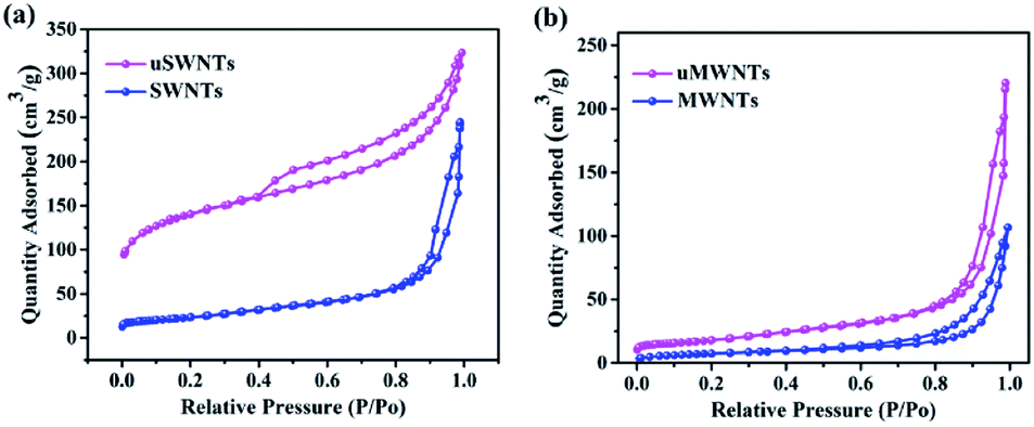 | ||
| Fig. 5 Nitrogen adsorption–desorption curve of (a) SWNTs and uSWNTs, (b) MWNTs and uMWNTs. | ||
To further study the chemical bonding of SWNTs and MWNTs in the oxidized state, we carried out XPS characterization of the SWNTs, MWNTs, uSWNTs, and uMWNTs. The ratio of the peak intensity of C 1s to the peak intensity of O 1s (C/O ratio) in the XPS spectrum of carbon materials is an indicator of the degree of oxidation of carbon materials.11,30,31,36 The XPS quantification result is summarized in Table 1. It shows that the C/O ratio decreases after unzipping, indicating that the degree of oxidation of the uSWNTs and uMWNTs increases. The C 1s spectra of MWNTs before and after oxidation (Fig. 6(c) and (d)) can be divided into four peaks, graphite-like sp2-C or sp3-C (CC), the epoxy group (C–O), the carbonyl group (CO), and the carboxyl group (O–CO). Fig. 5(a) gives C 1s spectra of pristine SWNTs indicating two peaks centered at 284.74 and 285.52 eV which are attributed to graphite-like sp2-C or sp3-C (CC) and epoxy groups (C–O). Unzipping the SWNTs results in appearing additional peaks as it follows from the data presented in Fig. 6(b). XPS of uSWNTs highlights presence of graphite-like sp2-C or sp3-C (CC) at 284.76 eV, epoxy group (C–O) at 286.52 eV, carbonyl group (CO) at 287.11 eV, and carboxyl group (O–CO) at 288.60 eV. XPS study supports that uSWNTs have a large number of carboxyl and hydroxyl groups.11 This observation is consistent with the result of FTIR shown in Fig. 3(a). Compared to the pristine SWNTs, strong peaks appear at 1614 cm−1 and 3438 cm−1 for uSWNTs, which are assigned to a CO and COO–H/O–H stretch. That verifies the carboxyl and hydroxyl functionalities are presented on the surface of uSWNTs. An attach of oxygen atoms to the nanotube walls would distort neighbouring CC double bond, which makes them more easily to be oxidized resulting in the nanotube opening.37 Therefore, the unzipping of SWNTs appears due to the attached epoxy, carbonyl, and carboxyl groups on the defective sites and edges of SWNTs. After unzipping, the amount of oxygen-containing functional groups and, particularly, carbonyl groups, increases significantly for uSWNTs contrarily to uMWNTs. Therefore, the number of defects introduced into uSWNTs is much more higher compared to uMWNTs. Moreover, compared to uMWNTs, the uSWNTs tend to be amorphous, which is consistent with the Raman and XRD data. Based on these observations, we suggested that uSWNTs blended with PEDOT:PSS as HTL on PSCs.
| Sample | O% | C% | C/O |
|---|---|---|---|
| SWNTs | 12.39 | 87.07 | 6.73 |
| uSWNTs | 42.10 | 57.90 | 1.38 |
| MWNTs | 1.73 | 98.27 | 57.10 |
| uMWNTs | 31.53 | 68.47 | 2.17 |
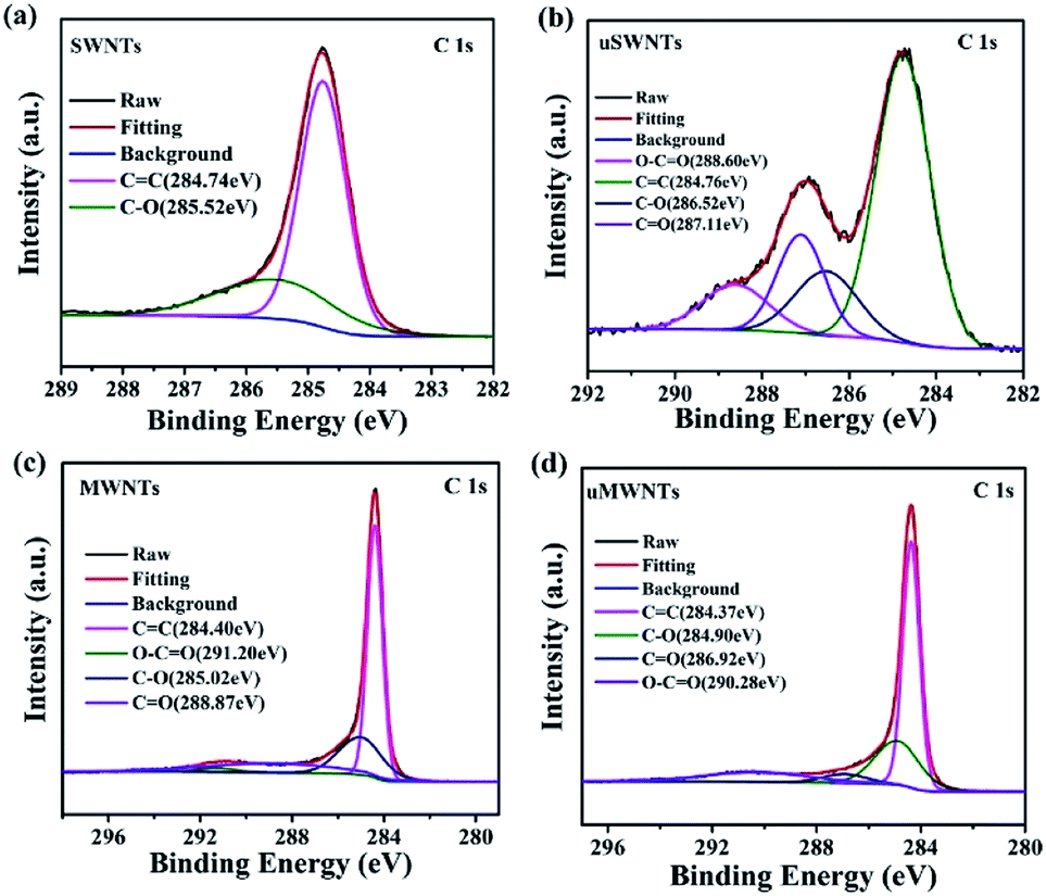 | ||
| Fig. 6 XPS C 1s spectra of (a) pristine SWNTs, (b) uSWNTs, (c) pristine MWNTs and (d) uMWNTs. | ||
Before the fabrication of the devices, we investigated the optical characteristics of the HTLs on ITO. The optical transparency of HTLs is an important factor determining photocurrent to absorb maximum light by photo-active layer. The transmittance spectra of all three types of HTLs along with bare ITO are shown in Fig. 7. All of the HTLs are highly transparent in the overall wavelength range with transmittance values up to 85% and do not significantly alter the transparency of ITO. Furthermore, the transmittance spectra of the ITO/PEDOT:PSS and ITO/uSWNTs/PEDOT:PSS is almost 15% higher compared to the transmittance of pure ITO and ITO/uSWNTs in the region of ∼400–500 nm. The difference of transmittance in the ∼400–500 nm region could potentially bring a significant effect on the photo-generated current (Jsc) of the device. Therefore, better efficiency is expected for ITO/PEDOT:PSS and ITO/uSWNTs/PEDOT:PSS, in good agreement with the photovoltaic studies of similar devices.19,21,38
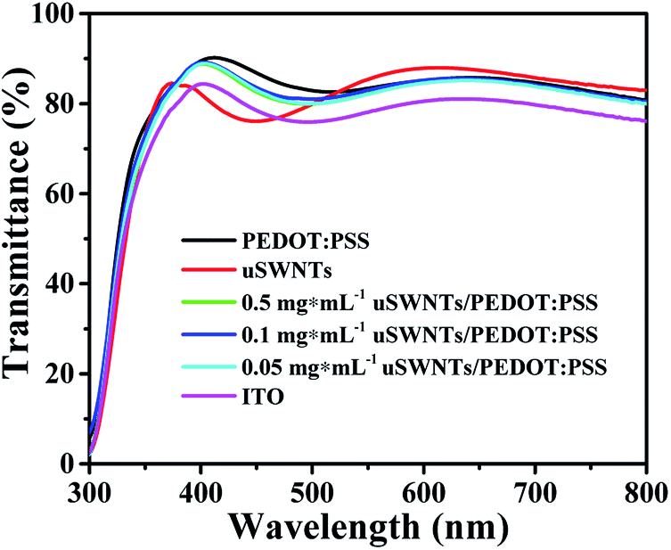 | ||
| Fig. 7 Transmittance spectra of ITO glass, ITO coated with pure PEDOT:PSS, uSWNTs, and uSWNTs/PEDOT:PSS with different concentrations. | ||
Fig. 8(a) shows the typical current density–voltage (J–V) characteristics under the illumination of the PBDB-T-2F:IF-4F device with uSWNTs, pure PEDOT:PSS, and uSWNTs/PEDOT:PSS with different concentrations of uSWNTs. The key parameters of the devices are summarized in Table 2. The J–V curves indicate that the device with single uSWNTs exhibited poor performance with an open circuit voltage (Voc) of 0.512 V, a short-circuit current (Jsc) of 21.50 mA cm−2, a fill factor (FF) of 53.94%, and a power conversion efficiency (PCE) of 5.93%. The reason is mainly attributed to inhomogeneity of the uSWNTs layer which high surface roughness results in inefficient transportation of holes. The device with pure PEDOT:PSS as a HTL exhibited a relatively low performance with a Voc of 0.856 V, a Jsc of 22.16 mA cm−2, a FF of 72.35%, and a PCE of 13.72%. The devices using the concentrations at 0.5 mg mL−1 or 0.05 mg mL−1 of the uSWNTs/PEDOT:PSS double-decked HTL showed a low performance with PCE of 13.42% or 13.69%. The reason is mainly attributed to the too high or too low concentration of uSWNTs, result in inhomogeneity of the uSWNTs/PEDOT:PSS affect transportation of hole transport. In comparison, the devices using the concentrations at 0.1 mg mL−1 of the uSWNTs/PEDOT:PSS double-decked HTL showed superior performance with a Voc of 0.853 V, a Jsc of 23.39 mA cm−2, a FF of 73.17%, and a higher PCE of 14.60%. For the devices based on uSWNTs/PEDOT:PSS HTL, the improvement is attributable to high Jsc, FF, and Voc values as compared to either uSWNTs or pure PEDOT:PSS HTLs. Perhaps, a change in the devise performance is mainly associated with the ability of the oxygen-containing polar groups of uSWNTs to improve the compatibility between uSWNTs and PEDOT:PSS polar environment. As a result, uSWNTs/PEDOT:PSS hybrid layer does not destroy the structure of the heterojunction. Moreover, that can sufficiently block electrons and may partially inhibit ITO/PBDB-T-2F:IF-4F from forming an interface through the gap of uSWNTs, reinforcing the carrier collection in uSWNTs/PEDOT:PSS devices.
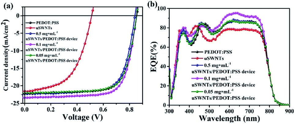 | ||
| Fig. 8 (a) Current density versus voltage characteristics. (b) External quantum efficiency (EQE) curves of devices using uSWNTs/PEDOT:PSS (different concentrations) as cathode buffer layers. | ||
| HTL configuration | Conductivity (S cm−1) | Voc (V) | Jsc (mA cm−2) | FF (%) | PCE (%) | Rs (Ω cm−2) |
|---|---|---|---|---|---|---|
| PEDOT:PSS | 1.968 | 0.856 | 22.16 | 72.35 | 13.72 | 3.75 |
| uSWNTs | 0.002 | 0.512 | 21.50 | 53.94 | 5.93 | 7.31 |
| 0.5 mg mL−1 uSWNTs/PEDOT:PSS | 1.724 | 0.842 | 22.33 | 71.38 | 13.42 | 4.14 |
| 0.1 mg mL−1 uSWNTs/PEDOT:PSS | 2.083 | 0.853 | 23.39 | 73.17 | 14.60 | 3.08 |
| 0.05 mg mL−1 uSWNTs/PEDOT:PSS | 2.041 | 0.854 | 22.12 | 72.53 | 13.69 | 3.45 |
The uSWNTs/PEDOT:PSS HTL exhibited an increase in conductivity compared to uSWNTs or PEDOT:PSS single HTLs as it follows from the data presented in Table 2. Measuring the conductivity of uSWNTs, pure PEDOT:PSS, and uSWNTs/PEDOT:PSS with different uSWNTs concentrations reveals that the conductivity is extremely low if only uSWNTs is used, whereas the conductivity of pure PEDOT:PSS and uSWNTs/PEDOT:PSS is almost the same. The conductivity of uSWNTs/PEDOT:PSS layer at the uSWNTs concentration of 0.1 mg mL−1 is highest. The corresponding device exhibits the best photovoltaic performance of PSCs. The high conductivity of uSWNTs/PEDOT:PSS film may be associated with a low value of Rs.4,20,39,40 A relatively low value of Rs for uSWNTs/PEDOT:PSS HTL demonstrates the improved charge transfer efficiency, which suggests the better charge transportation ability of the double-decked structure compared to single uSWNTS and pure PEDOT:PSS based devices.
To verify the high photocurrent density of uSWNTs/PEDOT:PSS devices, we measured the external quantum efficiency (EQE). Fig. 8(b) shows the EQE spectra of the PSCs based on the pure PEDOT:PSS and uSWNTs/PEDOT:PSS interlayer. Compared with the pure PEDOT:PSS cathode transport layer devices, the uSWNTs/PEDOT:PSS interlayer-based device has significantly enhanced EQE in the 500–770 nm wavelength range, indicating that the uSWNTs/PEDOT:PSS device has a lager Jsc, following the measured photocurrent density.7,41–43 It shows that the formation of uSWNTs/PEDOT:PSS structure increases the photocurrent density and enhance the EQE. In summary, uSWNTs/PEDOT:PSS device can effectively enhance the hole transport effect of PSCs resulting in higher Jsc, and EQE due to the improvement of the hole transport layer.
In order to confirm the repeatability of using uSWNTs/PEDOT:PSS HTLs, we recorded the photovoltaic parameters of uSWNTs/PEDOT:PSS devices with a concentration of 0.1 mg mL−1 and presented in Fig. 9. Devices based on uSWNTs/PEDOT:PSS and PEDOT:PSS exhibited excellent repeatability and reliability with very little change in Voc, FF and PCE. On the contrary, devices with uSWNTs showed relatively wide variations attributed to inhomogeneity of the uSWNTs results in inefficient transportation of holes.
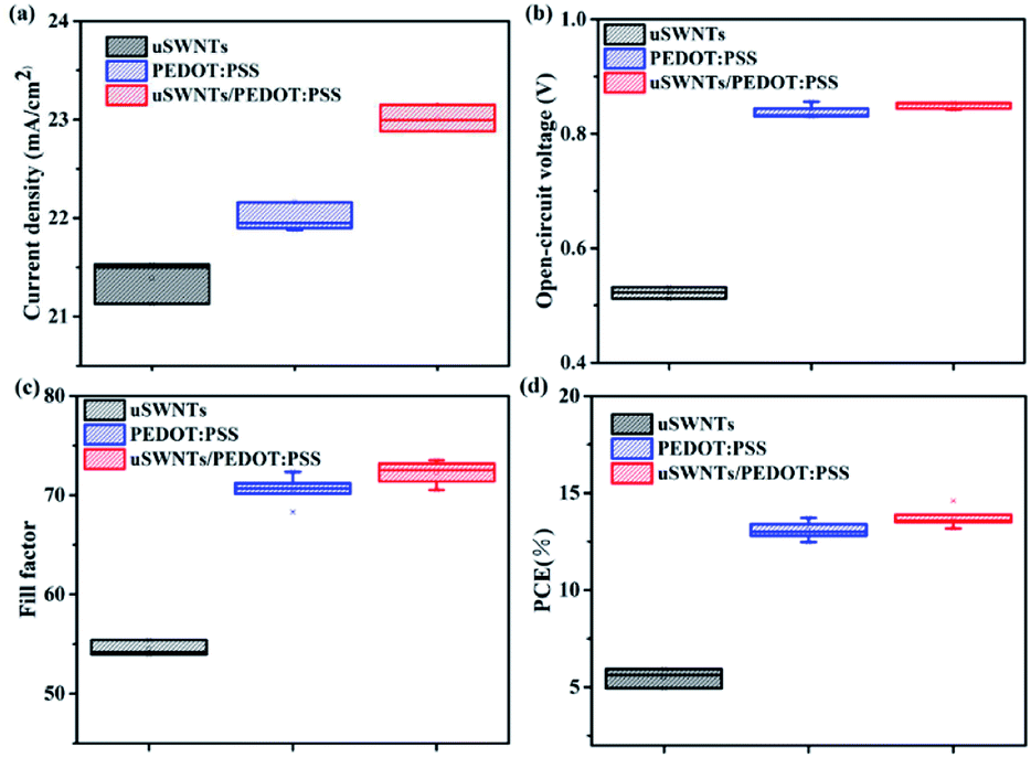 | ||
| Fig. 9 Photovoltaic performance parameters including (a) Jsc, (b) Voc, (c) FF and (d) PCE (%). | ||
The selection of the double-decked uSWNTs/PEDOT:PSS as HTL played a vital role in improving the efficiency and stability of the device. Using a single uSWNTs or pure PEDOT:PSS as the HTL in PSCs may cause serious instability issues at the anode interface. The acidic and hygroscopic PEDOT:PSS aqueous solution may react with ITO and the photosensitive layer. Identically, a single uSWNTs layer may cause uneven coatings on ITO, which would directly contact ITO and the photosensitive layer in uncovered areas and enormously reduces device performance. However, the combination of uSWNTs and PEDOT:PSS in a double-decked structure is a compatible solution to improve the deficiencies of both materials.
4. Conclusions
In this work, we demonstrated a facile method to fabricate an effective hole transport layer of uSWNTs/PEDOT:PSS to enhance the photovoltaic performances as an efficient HTL for highly efficient and stable PSCs. The uSWNTs/PEDOT:PSS is a promising candidate to replace conventional PEDOT:PSS or single uSWNTs HTL by complimenting the defects of both materials. Compared with traditional PEDOT:PSS, the uSWNTs/PEDOT:PSS, obtained by mixing the concentrations at 0.1 mg mL−1 of uSWNTs with PEDOT:PSS in a volume ratio of 7:3, results in a highly stable device. It demonstrates a Jsc = 23.39 mA cm−2, Voc = 0.853 V, FF = 73.17%, and PCE = 14.60%. The improved performance is also attributed to the increased conductivity and hole transport efficiency, which can be highly desired for carrier transportation and collection as evident from charge carrier mobility results. Moreover, the insensitivity of performances depending on thickness promises that the facile fabricated uSWNTs/PEDOT:PSS layer has more potential to apply to the future roll-to-roll process of PSCs with extremely low cost. Therefore, our study shows that uSWNTs/PEDOT:PSS nanocomposites can be used as HTL for high-performance and reliable PSCs.
Conflicts of interest
There are no conflicts to declare.Acknowledgements
This work was supported by National Natural Science Foundation of China (51473082), State Key Project of International Cooperation Research (2017YFE0108300, 2016YFE0110800), the National High-End Foreign Expert of China, the Program for Introducing Talents of Discipline to Universities (“111” plan), 1st class discipline program of Materials Science of Shandong Province, and Qingdao Basic research on application of science and technology plan (19-6-2-82-cg).Notes and references
- E. Kymakis, G. Klapsis, E. Koudoumas, E. Stratakis, N. Kornilios, N. Vidakis and Y. Franghiadakis, Eur. Phys. J.: Appl. Phys., 2007, 36, 257–259 CrossRef.
- Y. Wang, H. Wang, J. Xu, B. He, W. Li, Q. Wang, S. Yang and B. Zou, Polym. Compos., 2018, 39, 3066–3072 CrossRef CAS.
- Y. Zhang, H. Yao, S. Zhang, Y. Qin, J. Zhang, L. Yang, W. Li, Z. Wei, F. Gao and J. Hou, Sci. China: Chem., 2018, 61, 1328–1337 CrossRef CAS.
- J. Niu, D. Yang, X. Ren, Z. Yang, Y. Liu, X. Zhu, W. Zhao and S. Liu, Org. Electron., 2017, 48, 165–171 CrossRef CAS.
- S. Yoon, H. Kim, E.-Y. Shin, Y.-Y. Noh, B. Park and I. Hwang, Phys. Status Solidi A, 2016, 213, 2431–2437 CrossRef CAS.
- W. Shen, W. Chen, X. Xu, D. Zhu and J. Zhang, J. Mater. Chem. A, 2017, 5, 12400–12406 RSC.
- J. C. Yu, J. A. Hong, E. D. Jung, D. B. Kim, S. M. Baek, S. Lee, S. Cho, S. S. Park, K. J. Choi and M. H. Song, Sci. Rep., 2018, 8, 1070 CrossRef PubMed.
- P. C. Mahakul, K. Sa, B. Das, B. V. R. S. Subramaniam, S. Saha, B. Moharana, J. Raiguru, S. Dash, J. Mukherjee and P. Mahanandia, J. Mater. Sci., 2017, 52, 5696–5707 CrossRef CAS.
- W. Shen, Int. J. Electrochem. Sci., 2017, 12, 6676–6693 CrossRef CAS.
- R. C. Shende and S. Ramaprabhu, Sol. Energy Mater. Sol. Cells, 2016, 157, 117–125 CrossRef CAS.
- D. Torres, J. L. Pinilla and I. Suelves, Appl. Surf. Sci., 2017, 424, 101–110 CrossRef CAS.
- I. Janowska, O. Ersen, T. Jacob, P. Vennégues, D. Bégin, M.-J. Ledoux and C. Pham-Huu, Appl. Catal., A, 2009, 371, 22–30 CrossRef CAS.
- I. Jeon, R. Xiang, A. Shawky, Y. Matsuo and S. Maruyama, Adv. Energy Mater., 2018, 9, 1801312 CrossRef.
- D. V. Kosynkin, A. L. Higginbotham, A. Sinitskii, J. R. Lomeda, A. Dimiev, B. K. Price and J. M. Tour, Nature, 2009, 458, 872–876 CrossRef CAS PubMed.
- D. Wei, L. Xie, K. K. Lee, Z. Hu, S. Tan, W. Chen, C. H. Sow, K. Chen, Y. Liu and A. T. Wee, Nat. Commun., 2013, 4, 1374 CrossRef PubMed.
- D. B. Shinde, M. Majumder and V. K. Pillai, Sci. Rep., 2014, 4, 4363 CrossRef PubMed.
- J. Lim, U. N. Maiti, N. Y. Kim, R. Narayan, W. J. Lee, D. S. Choi, Y. Oh, J. M. Lee, G. Y. Lee, S. H. Kang, H. Kim, Y. H. Kim and S. O. Kim, Nat. Commun., 2016, 7, 10364 CrossRef CAS PubMed.
- L. Jiao, L. Zhang, X. Wang, G. Diankov and H. Dai, Nature, 2009, 458, 877–880 CrossRef CAS PubMed.
- X. Huang, H. Guo, J. Yang, K. Wang, X. Niu and X. Liu, Org. Electron., 2016, 39, 288–295 CrossRef CAS.
- G.-H. Jeong, S.-J. Kim, H.-S. Ko, E.-M. Han and K. H. Park, Mol. Cryst. Liq. Cryst., 2015, 620, 117–122 CrossRef CAS.
- D. Y. Lee, S. I. Na and S. S. Kim, Nanoscale, 2016, 8, 1513–1522 RSC.
- S. Yoon, S. R. Ha, T. Moon, S. M. Jeong, T.-J. Ha, H. Choi and D.-W. Kang, J. Power Sources, 2019, 435, 226765 CrossRef CAS.
- S. AbdulAlmohsin and J. B. Cui, J. Phys. Chem. C, 2012, 116, 9433–9438 CrossRef CAS.
- W. Shen, J. Tang, D. Wang, R. Yang, W. Chen, X. Bao, Y. Wang, J. Jiao, Y. Wang, R. Yang, J. Yun and L. A. Belfiore, Mater. Sci. Eng., B, 2016, 206, 61–68 CrossRef CAS.
- Y. Xia, Y. Pan, H. Zhang, J. Qiu, Y. Zheng, Y. Chen and W. Huang, ACS Appl. Mater. Interfaces, 2017, 9, 26252–26256 CrossRef CAS PubMed.
- W. Shen, J. Tang, Y. Wang, J. Liu, L. Huang, W. Chen, L. Yang, W. Wang, Y. Wang and R. Yang, ACS Appl. Mater. Interfaces, 2017, 9, 5358–5365 CrossRef CAS PubMed.
- W. Shen, C. Yang, X. Bao, L. Sun, N. Wang, J. Tang, W. Chen and R. Yang, Mater. Sci. Eng., B, 2015, 200, 1–8 CrossRef CAS.
- W. Chen, W. Shen, H. Wang, F. Liu, L. Duan, X. Xu, D. Zhu, M. Qiu, E. Wang and R. Yang, Dyes Pigm., 2019, 166, 42–48 CrossRef CAS.
- W. E. Mahmoud, F. S. Al-Hazmi and G. H. Al-Harbi, Chem. Eng. J., 2015, 281, 192–198 CrossRef CAS.
- C.-I. Chang, K.-H. Chang, H.-H. Shen and C.-C. Hu, J. Taiwan Inst. Chem. Eng., 2014, 45, 2762–2769 CrossRef CAS.
- D. Torres, J. L. Pinilla, R. Moliner and I. Suelves, Carbon, 2015, 81, 405–417 CrossRef CAS.
- V. Gupta, N. Sharma, U. Singh, M. Arif and A. Singh, Optik, 2017, 143, 115–124 CrossRef CAS.
- S. Schöche, N. Hong, M. Khorasaninejad, A. Ambrosio, E. Orabona, P. Maddalena and F. Capasso, Appl. Surf. Sci., 2017, 421, 778–782 CrossRef.
- H.-C. Youn, S.-H. Park, K. C. Roh and K.-B. Kim, Curr. Appl. Phys., 2015, 15, S21–S26 CrossRef.
- S. Cho, K. Kikuchi and A. Kawasaki, Carbon, 2011, 49, 3865–3872 CrossRef CAS.
- S. R. Dhakate, N. Chauhan, S. Sharma and R. B. Mathur, Carbon, 2011, 49, 4170–4178 CrossRef CAS.
- C. Wang, Y. S. Li, J. Jiang and W. H. Chiang, ACS Appl. Mater. Interfaces, 2015, 7, 17441–17449 CrossRef CAS PubMed.
- S. Rafique, S. M. Abdullah, M. M. Shahid, M. O. Ansari and K. Sulaiman, Sci. Rep., 2017, 7, 39555 CrossRef CAS PubMed.
- S. Chen, X. Yu, M. Zhang, J. Cao, Y. Li, L. Ding and G. Shi, J. Mater. Chem. A, 2015, 3, 18380–18383 RSC.
- X. Huang, H. Yu, Z. Wu and Y. Li, J. Solid State Electrochem., 2017, 22, 317–329 CrossRef.
- B. Sun, D. Zhou, C. Wang, P. Liu, Y. Hao, D. Han, L. Feng and Y. Zhou, Org. Electron., 2017, 44, 176–182 CrossRef CAS.
- H. Luo, X. Lin, X. Hou, L. Pan, S. Huang and X. Chen, Nano-Micro Lett., 2017, 9, 39 CrossRef PubMed.
- F. Bu, W. Shen, X. Zhang, Y. Wang, L. A. Belfiore and J. Tang, Nanomaterials, 2020, 10, 80 CrossRef CAS PubMed.
Footnote |
| † Wenna Zhang and Fanchen Bu contributed equally to this work. |
| This journal is © The Royal Society of Chemistry 2020 |