DOI:
10.1039/D0RA03364B
(Paper)
RSC Adv., 2020,
10, 28766-28777
The influence of the interfacial layer on the stability of all-solution-processed organic light-emitting diodes†
Received
15th April 2020
, Accepted 6th July 2020
First published on 3rd August 2020
Abstract
Improving the stability of large-area organic light-emitting diodes is very important for practical applications. The interfacial layer plays a crucial role to improve the electron injection characteristic. In this work, devices prepared by various solution-processed interfacial materials and thermal-evaporated CsF were compared. In the devices with active area of 2.25 mm × 2.25 mm, we found that the performance and lifetime of the device with solution-processed Liq interfacial layer was comparable with the device with thermal-evaporated CsF. However, for the devices with active area of 2.4 cm × 3.7 cm, the device based on thermal-evaporated CsF was the champion in both performance and lifetime. The influence of the thickness of CsF on the stability was investigated. The most stable blue fluorescent devices can be achieved when the thickness of CsF is about 0.1 nm, while the most stable green phosphorescent devices can be obtained by depositing 0.2 nm CsF. The best current efficiency for the blue fluorescent device is 4 cd A−1, while the best one for the green phosphorescent device is 22 cd A−1. Furthermore, burning points causing the failure of the devices were investigated by scanning electron microscopy, atomic force microscopy, thermography and secondary ion mass spectrometry. We demonstrated that burning points are defects, which can be observed after long-time operation, showing higher local temperature and fragmentary electrode.
1. Introduction
In the field of the organic light-emitting diodes (OLEDs), low work function metals have been used as cathodes to reduce electron injection barrier.1,2a–d However, low work function metals, such as calcium, are susceptible to atmospheric moisture and oxygen, causing stability issues. Aluminum (Al) has been extensively used as cathode because of its stability in air. However, the work function of Al is 4.3 eV, causing a high electron injection barrier.3 Conventionally, to reduce the electron injection barrier, a very thin interfacial dipole layer between Al electrode and organic layer is used.4,5 The interfacial dipole layer can be prepared by thermal evaporation or solution process.6–10 However, for large-area OLEDs, there are still many problem needed to be solved to realize devices with solution-processed interfacial layers.
We have studied all-solution-processed large-area OLEDs without electron transport layer.11 The electron transport material, 2,7-bis(diphenylphosphoryl)-9,9′-spirobifluorene (SPPO13) was doped into the emission layer for electron–hole balance. This simple device structure make the fabrication process easier. The mechanism of operation of LiF/Al and CsF/Al cathode in OLEDs have been widely investigated.12–22 The current efficiency of CsF/Al cathode is better than that of LiF/Al cathode.23,24 When CsF film is deposited between Al and organic layer, Al reacts and dissociates CsF to form AlF3, releasing metallic Cs. Then, the metallic Cs dopes the organic layer and forms ohmic contact.25
Large-area and solution-processed devices have many applications.26,27 Many interfacial materials had been investigated as cathode modification interlayer of semiconductor devices so far.4,5,28–33 The advantage of a solution-processed cathode modification interlayer is that some materials can be doped into an interfacial layer, which can help to produce beneficial reaction between an interfacial layer and cathode. In accordance with these references, we investigated interfacial layers with a solution-processed blade coating. In this work, four types materials were used and compared for large-area (3.7 cm × 2.4 cm) and small-area (2.25 mm × 2.25 mm) blue fluorescent OLEDs and green phosphorescent OLEDs: (i) solution-processed metallic salt, cesium carbonate (Cs2CO3), 8-hydroxyquinolato lithium (Liq), lithium nitride (Li3N) and lithium phenolate complexes (Libpp), (ii) expensive solution-processed conjugated organic molecules, poly[(9,9-bis(3-(N,N-dimethylamino)propyl)-2,7-fluorene)-alt-2,7-(9,9-dioctylfluorene)] (PFN-Br), (iii) cheap solution-coated non-conjugated organic molecules, polyethylene glycol (PEG), and (iv) evaporated metallic salt, cesium fluoride (CsF). The commonly used materials in these four material types were selected. The performance and lifetime of large-area devices with various CsF thickness were also compared. Finally, the defect, called burning points, were investigated by scanning electron microscopy (SEM), atomic force microscopy (AFM), thermography and secondary ion mass spectroscopy (SIMS).
2. Results and discussion
2.1 Solution-processed versus thermal-evaporated interfacial materials
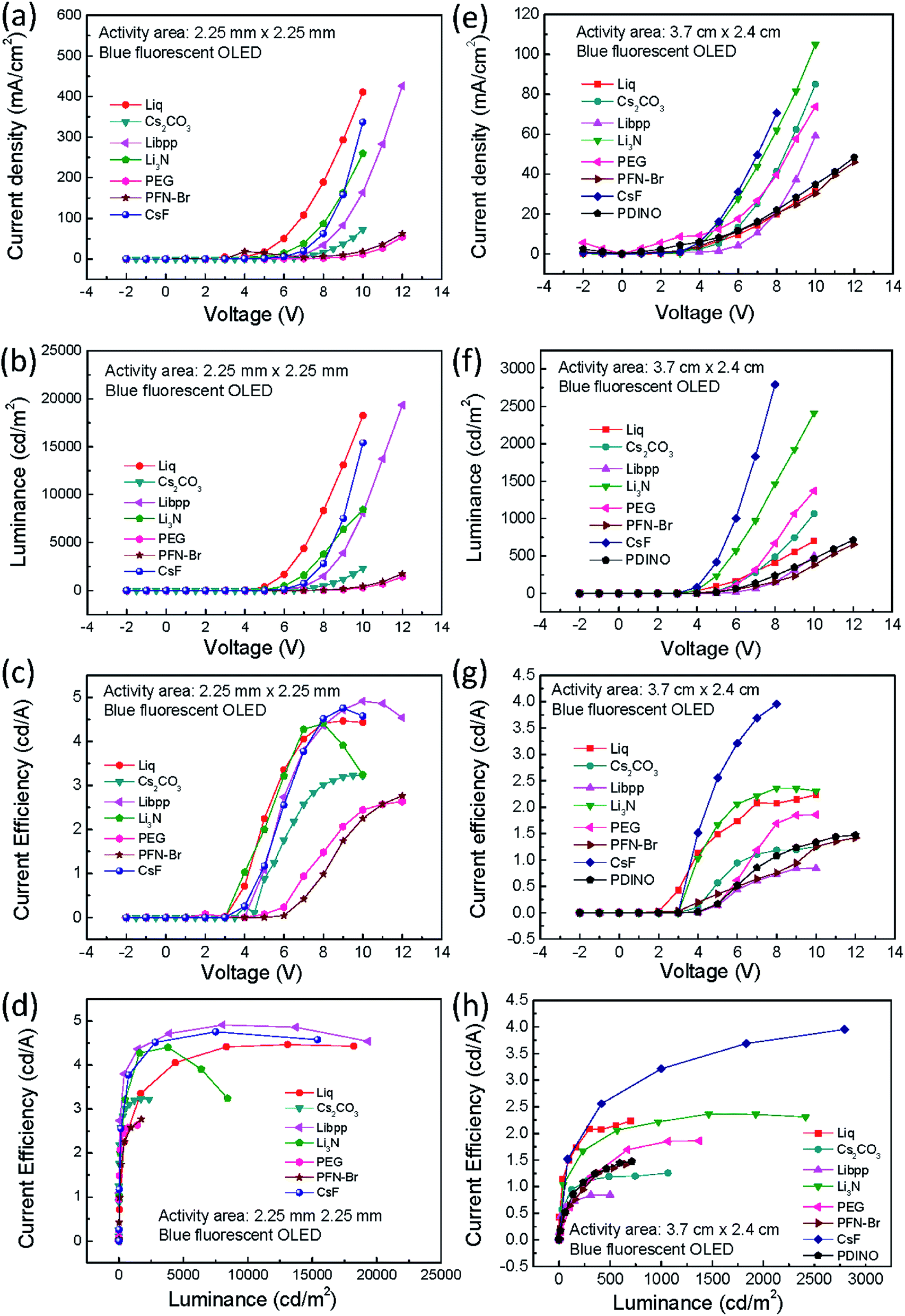
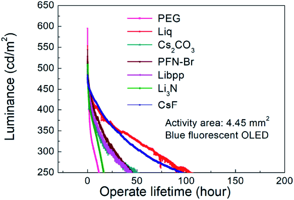
To understand the influence of interfacial layer on the performance of the OLEDs, many materials were used as the interfacial layer for comparison. All the fabrication procedures of the devices were the same, excepting the materials used for the interfacial layer. The chemical structures of the materials used in this work are shown in Fig. 1. Both large-area (3.7 cm × 2.4 cm) and small-area (2.25 mm × 2.25 mm) OLEDs were prepared and compared. The device structure and the energy level diagram of the device are shown in Fig. 2a and b, respectively. The active area of the large-area device was determined by depositing an insulating SiO layer surrounding the active area, as shown in Fig. S1.† In this way, the leakage current at the boundary of the active area can be reduced, and the efficiency of the large-area devices with a SiO layer was demonstrated to be better than the devices without a SiO layer.34 The devices structure are ITO/PEDOT:PSS(100 nm)/TFB(10 nm)/PT-404:SPPO13:Blue D (90 nm)/interfacial layer (5 nm)/Al (100 nm). The devices were prepared by blade coating method published before.11,35–39 The performance of small-area devices (large-area devices) with various interfacial materials are shown in Fig. 3a–d (Fig. 3e–h). For the small-area devices, the current density (Fig. 3a) of solution-processed Liq, Li3N, Libpp, and thermal evaporated CsF showed better electron injection than the others interfacial layers, leading to higher luminance (Fig. 3b) than the others interfacial layers. Furthermore, the current efficiency of the devices with solution-processed Liq, Libpp, and Li3N as the interfacial layer are comparable with the device with thermal-evaporated CsF. These devices shown current efficiency (Fig. 3c) and luminance (Fig. 3b) higher than 4 cd A−1 and 8000 cd m−2, respectively. The detailed small-area data of all interfacial layers were shown in Table 1. When considering the stability of the solution-processed devices, the device with Liq as the interfacial layer showed better stability, as shown in Fig. 4. The half-lifetime (LT50) the device with Liq as the interfacial layer is about 100 hours, which is comparable to the LT50 of the device with thermal-evaporated CsF.
 |
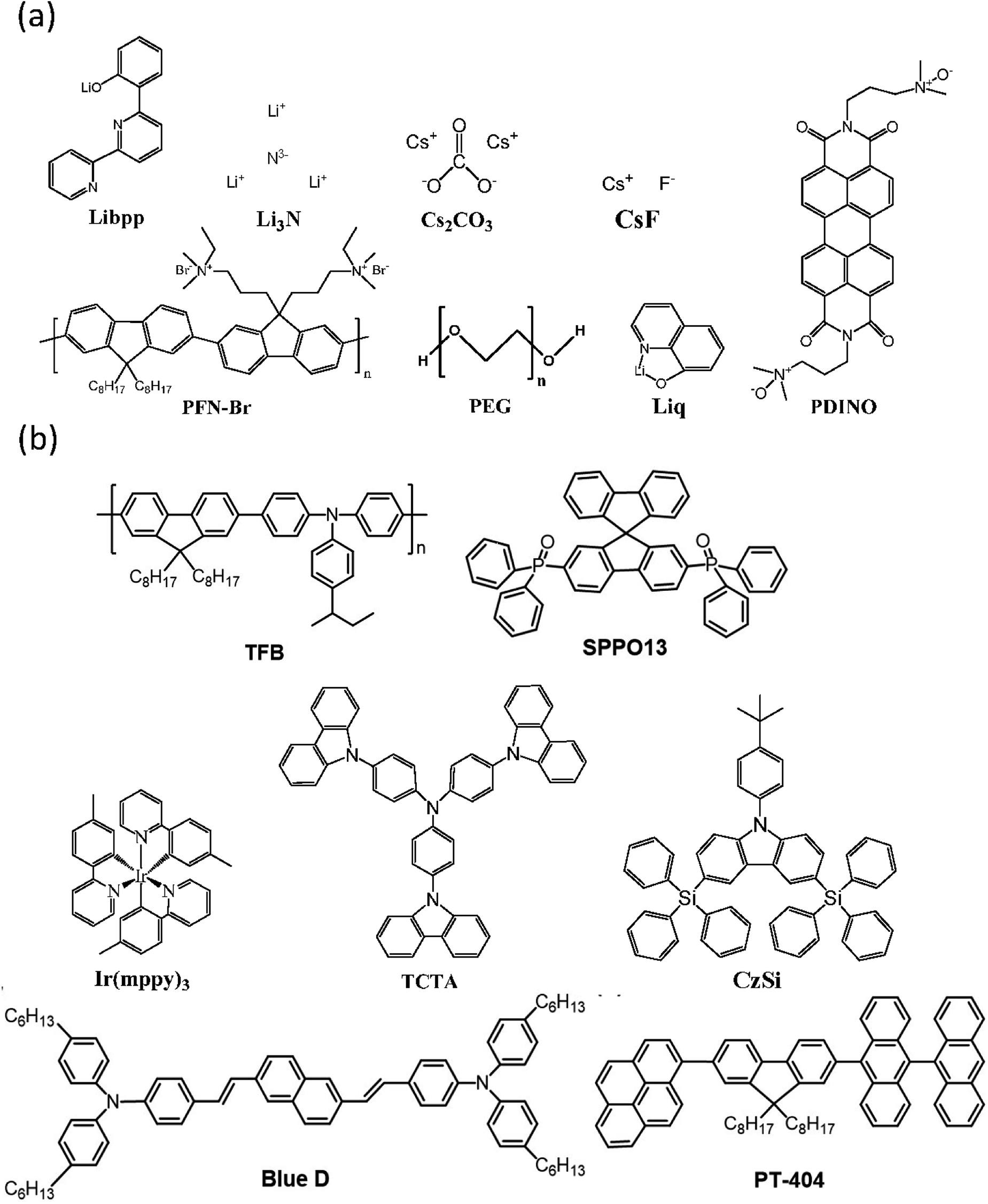
| | Fig. 1 The chemical structures of (a) the interfacial materials and (b) the materials used in the emission layer. | |
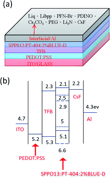 |
| | Fig. 2 (a) The schematic device structure and (b) the energy band diagram of the device. | |
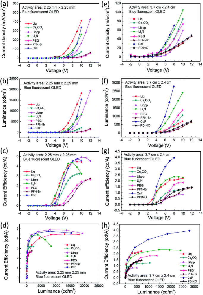 |
| | Fig. 3 (a) and (e) The current density versus voltage, (b) and (f) the luminance versus voltage, (c) and (g) the current efficiency versus voltage, and (d) and (h) the current efficiency versus luminance of the (a–d) small-area and (d–h) large-area blue OLEDs with different interfacial materials. | |
Table 1 OLED performance of small-area devices with various interfacial layers
| Materials |
5 V |
8 V |
| Current density (mA cm−2) |
Luminance (cd m−2) |
Current efficiency (cd A−1) |
Current density (mA cm−2) |
Current density (mA cm−2) |
Current efficiency (cd A−1) |
| Thermal-evaporated CsF |
1.96 |
22.92 |
1.117 |
62.3 |
2815 |
4.517 |
| Solution-processed Liq |
17.2 |
386.5 |
2.246 |
189 |
8334 |
4.414 |
| Cs2CO3 |
0.317 |
2.792 |
0.882 |
16.7 |
503.1 |
3.015 |
| Libpp |
0.867 |
9.397 |
1.084 |
33.9 |
1477 |
4.363 |
| Li3N |
5.14 |
102.6 |
1.997 |
86.4 |
3805 |
4.404 |
| PEG |
0.398 |
0.3055 |
0.077 |
2.19 |
32.36 |
1.48 |
| PFN-Br |
14.7 |
0.3501 |
0.002 |
6.51 |
64.03 |
0.983 |
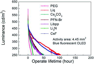 |
| | Fig. 4 The lifetime of the small-area blue fluorescent OLEDs with various interfacial materials. | |
However, due to the built-in resistance, the turned-on voltage of large-area devices became large so that the current density (Fig. 3e) and the luminance (Fig. 3f) of large-area devices are lower than that of small-area devices, contributing to lower current efficiency (Fig. 3g). Moreover, the performance of the devices with solution-processed interfacial layers is inferior to the performance of the device with thermal-evaporated CsF, as shown in Fig. 3e–h. The detailed large-area data of all interfacial layers were shown in Table 2. The reason for that is probably that thermal-evaporated interfacial material has better atomic arrangement than solution-processed interfacial layers in the large-area devices. Besides, the stability of the large-area devices with thermal-evaporated CsF are better than those with solution-processed interfacial layers, in which defects and decrease in luminescence can be observed on devices with solution-processed interfacial layers in a short time, as shown in Fig. 5. These defects might be attributed to the difficulty to control the uniformity and thickness of the solution-coated interfacial layer in the nanometer range. These results indicated that, for large-area applications, thermal-evaporated CsF is a better choice than all the other solution-processed materials tested in this work. Therefore, the influence of the thickness of the thermal-evaporated CsF on the performance of large-area green phosphorescent and blue fluorescent devices were investigated.
Table 2 OLED performance of large-area devices with various interfacial layers
| Materials |
5 V |
8 V |
| Current density (mA cm−2) |
Luminance (cd m−2) |
Current efficiency (cd A−1) |
Current density (mA cm−2) |
Current density (mA cm−2) |
Current efficiency (cd A−1) |
| Thermal-evaporated CsF |
16.2 |
415.6 |
2.558 |
70.7 |
2795 |
3.953 |
| Solution-processed Liq |
6.48 |
96.52 |
1.49 |
19.9 |
411.9 |
2.074 |
| Cs2CO3 |
5.29 |
29.96 |
0.567 |
41.3 |
490.1 |
1.187 |
| Libpp |
1.46 |
2.012 |
0.138 |
20.8 |
151.3 |
0.728 |
| Li3N |
14.1 |
234.7 |
1.669 |
62 |
1465 |
2.364 |
| PEG |
12.3 |
18.78 |
0.153 |
39.6 |
670.4 |
1.692 |
| PFN-Br |
7.34 |
26.14 |
0.356 |
20.4 |
154.7 |
0.759 |
| PDINO |
8.22 |
13.64 |
0.166 |
22 |
237.1 |
1.078 |
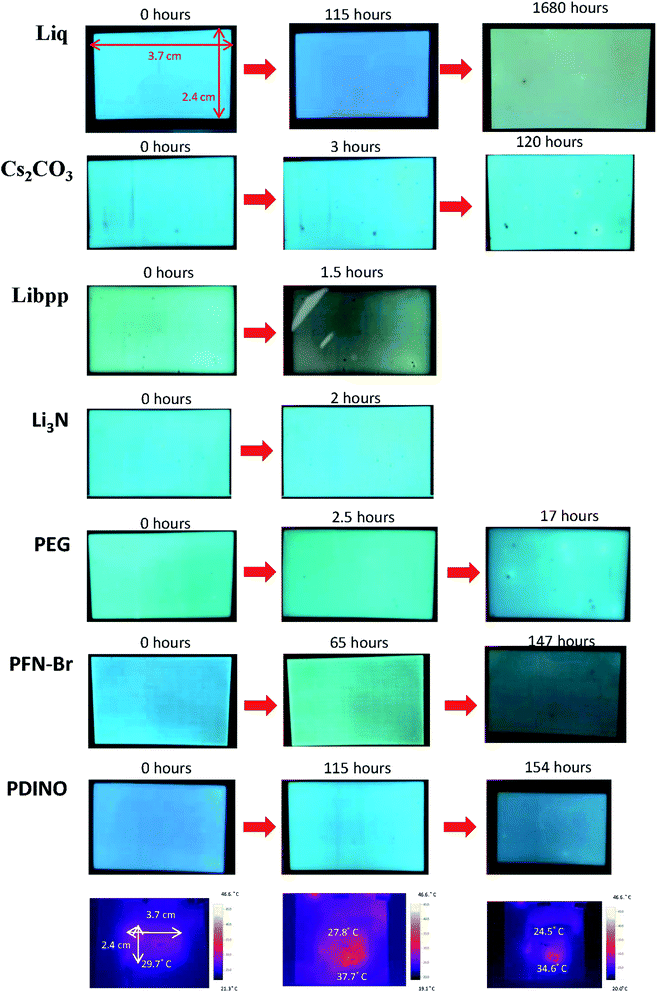 |
| | Fig. 5 The photographs of the large-area blue fluorescent OLEDs with various interfacial materials operating for a long time. | |
2.2 The influence of the thickness of CsF films
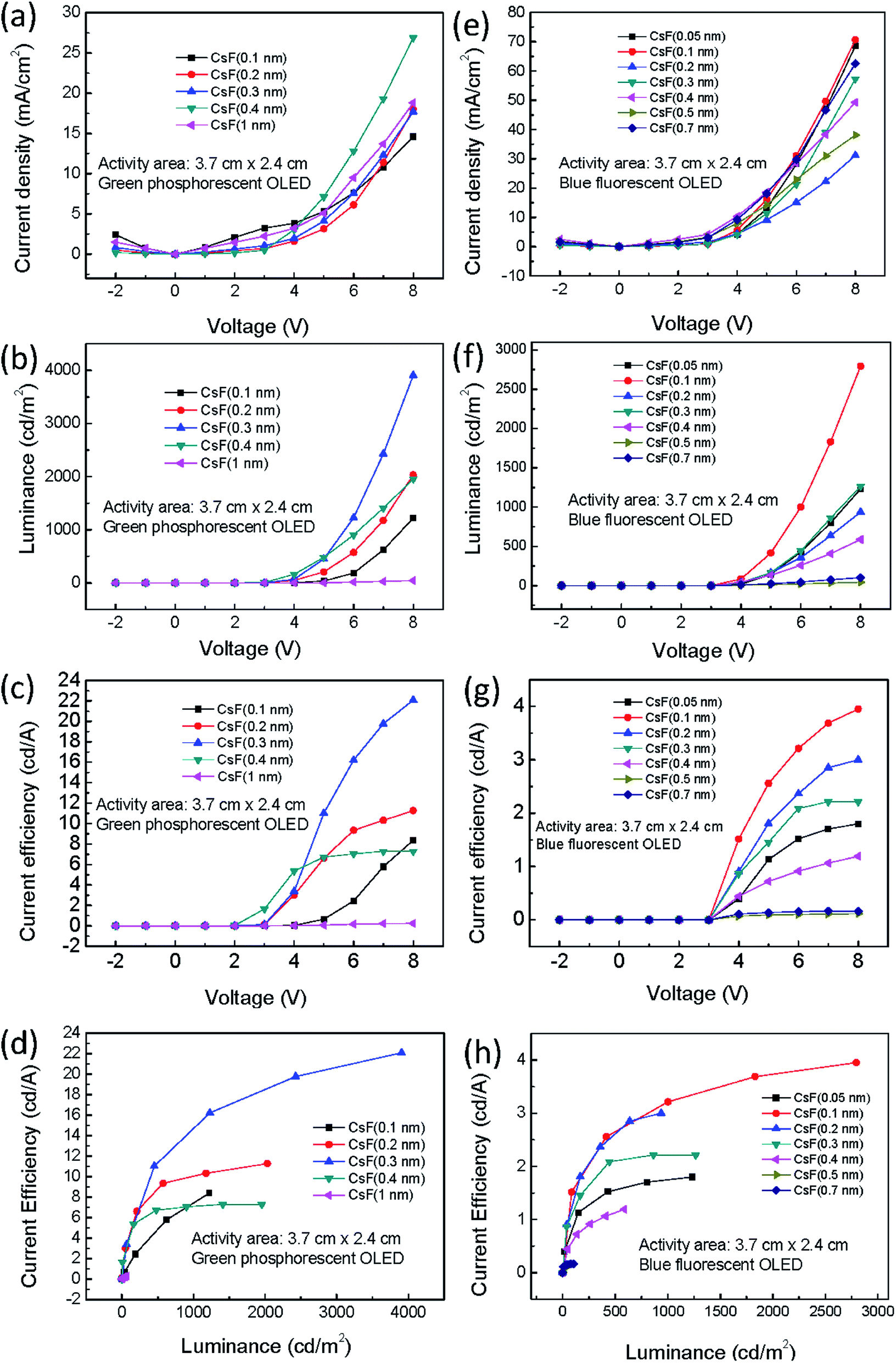
Green phosphorescent and blue fluorescent OLED large-area (3.7 cm × 2.4 cm) devices with various CsF thickness were fabricated to investigate the influence of CsF thickness on the device performance. The device performance of the green phosphorescent devices are shown in Fig. 6a–d, and the device performance of the blue fluorescent devices are shown in Fig. 6e–h. When the thickness of CsF thicker than 0.4 nm, both the green and blue devices showed poor performance. As shown in Fig. 6c, it was observed that the optimized CsF thickness and efficiency at 8 V for green phosphorescent devices was 0.3 nm and 22 cd A−1, respectively. As for the blue fluorescent devices, the optimized CsF thickness and efficiency was 0.1 nm and 4 cd A−1, as shown in Fig. 6g. The reproducibility of these devices with various CsF thicknesses are shown in Fig. S2–S13.†
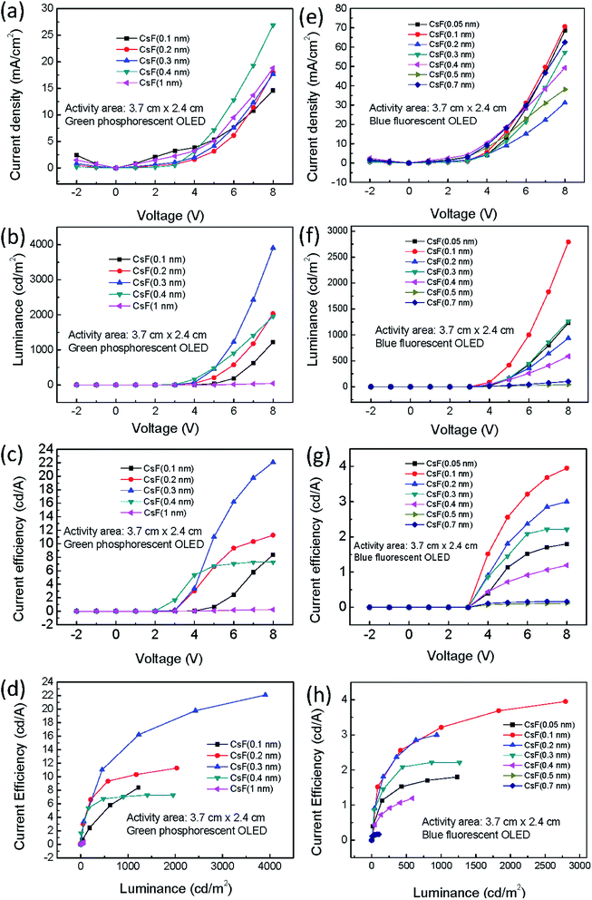 |
| | Fig. 6 (a) and (e) The current density versus voltage, (b) and (f) the luminance versus voltage, (c) and (g) the current efficiency versus voltage, and (d) and (h) the current efficiency versus luminance of the large-area (a–d) green and (d–h) blue OLEDs with different CsF thickness. | |
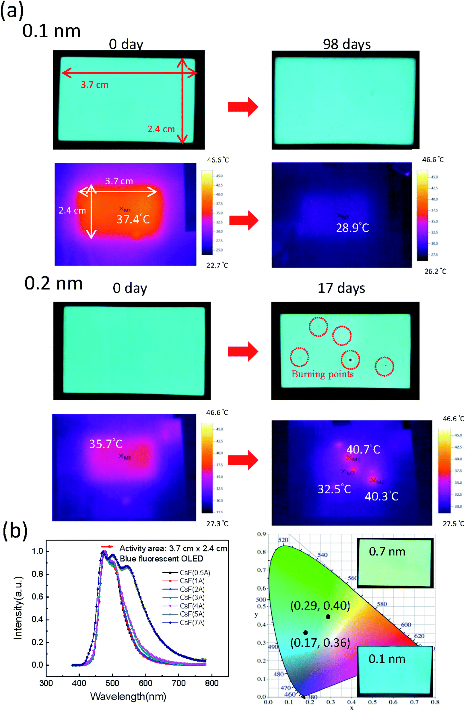
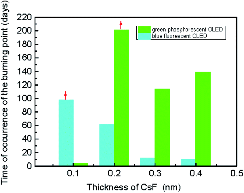
The stability of the large-area devices with thermal-evaporated CsF are also related to the thickness of CsF, as shown in Fig. 7, 8, S14 and S15.† The photograph and thermal image of the turned-on blue fluorescent OLED large-area device with optimized CsF thickness of 0.1 nm is shown in Fig. 7a. This device showed uniform emission and temperature distribution even after 98 days. However, for the device with other CsF thicknesses, the burning point appeared after long-tern operation. The influence of CsF thickness on the time when burning point was observed was shown in Fig. 8. The red arrows indicated that the number of days will continue to increase because those devices show no burning point so far. The best CsF thickness for blue fluorescent OLED devices to have a better stability is about 0.1 nm, while for green phosphorescent OLED devices the best CsF thickness is about 0.2 nm. Thick CsF induces the burning point easily. The thickness of CsF is also an influential factor to the electroluminescence (EL) spectra and CIE coordinates, as shown in Fig. 7b. Both the EL spectra and CIE coordinates are different for the device with CsF thicker and thinner than 0.4 nm. The CIE coordinates were changed from (0.17, 0.36) to (0.29, 0.40). Even though the device performance is relatively insensitive to the CsF thickness for the devices with CsF thickness thicker than 0.4 nm,25 the devices with thick CsF thickness in this work showed shifted spectra and high driving voltage making them meaningless. When the size was increased to 6 cm × 11.5 cm and the blue emitter was changed to EB-N02, the devices prepared with optimized conditions also functions very well, as shown Fig. S14.†
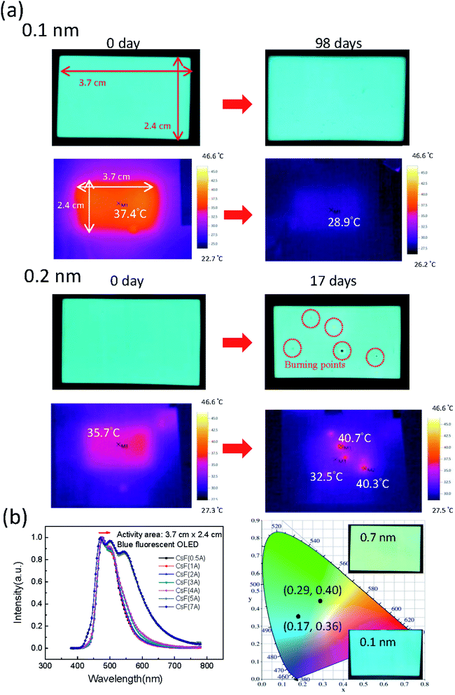 |
| | Fig. 7 (a) The photographs, thermal images, (b) spectra and CIE coordinates of the large-area blue OLEDs with different CsF thickness. | |
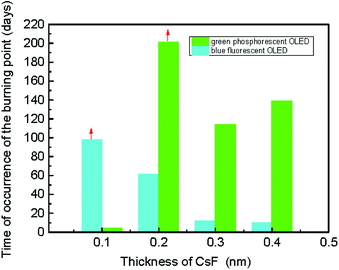 |
| | Fig. 8 The influence of the thickness of CsF on the time burning points can be observed in the large-area blue OLEDs. | |
The burning points mentioned above are different from the conventional black spots. The black spots mentioned in this work are not those spot in previous reports.40–43 The influence of the black spots on the OLED devices have been discussed in detail.40–43 The black spots in this work usually refer to the defects caused by dusts. After operating the devices for a long time, these black spots do not lead to high local current density and temperature. Therefore, black spots do not affect the long time-operating stability of devices. Controlling the fabrication conditions could eliminate black spots. However, the burning points mentioned in this work are local areas which cause leakage current and high temperature areas. When the devices are just turned on, these burning points cannot be observed. These burning points can only be observed after operating devices for a long time. Usually, a burning point show higher temperature with a bright circle surrounding a black area.
The above mentioned characteristics can also be observed for the green phosphorescent OLED devices, as shown Fig. S15.† The green phosphorescent device with optimized CsF thickness of 0.2 nm showed uniform emission and temperature distribution even after 180 days. Both the EL spectra and CIE coordinates changed dramatically when the thickness of CsF is thicker than 0.4 nm. The CIE coordinates were changed from (0.30, 0.61) to (0.28, 0.41).
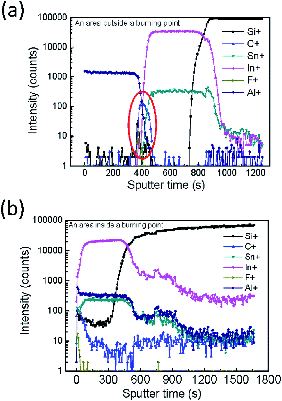
To further analyze the burning points, many images of the burning point were taken, as shown in Fig. 9. The burning point observed on a large-area device (Fig. 9a) was marked and cut into small pieces. The optical microscope image of the burning point showed that the aluminum electrode lose it reflectivity at the location of the burning point, indicating that there is a rough surface. The top-view scanning electron microscope (SEM) images (Fig. 9b) and atomic force microscopy (AFM) images (Fig. 9e) confirmed the rough surface at the burning point. The cross-sectional view SEM images further showed that the aluminum electrode was detached from the underlayer, as shown in Fig. 9c. However, the device structure at the place without burning point showed a flat and smooth layer-by-layer structure (Fig. 9d and f). Secondary ion mass spectroscopy (SIMS) showed signal from aluminum, fluoride, carbon and indium in sequence, indicating a sharp interface at the place without burning point (Fig. 10a). In contrast, at the place with burning point, SIMS showed all the signals in the beginning, indicating a broken and discontinue aluminum electrode (Fig. 10b). All these indicated that there might be a local high current density, leading to the high local temperature and the damage of the electrode.
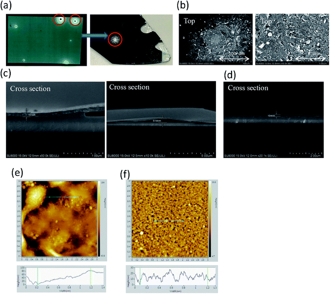 |
| | Fig. 9 (a) The photographs of the device with burning points. (b) The top-view SEM images and (c) side-view SEM images of a burning point. (d) The side-view SEM image of the device without burning point. The AFM image (e) inside and (f) outside the burning point. | |
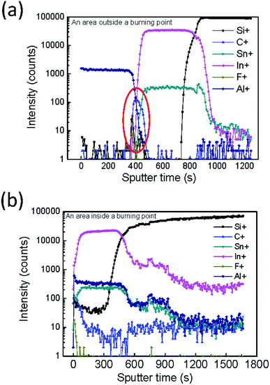 |
| | Fig. 10 The SIMS profiles (a) inside a burning point and (b) outside a burning point. | |
3. Conclusions
Various solution-processed interfacial materials were used as the interfacial layer in OLEDs. It was found that small-area devices based on Liq are comparable with small-area devices based on CsF. However, large-area devices based on CsF were superior to all the other devices with solution-processed interfacial layer. The influence of CsF thickness on the stability of large-area devices was investigated. The optimized CsF thicknesses were found for blue fluorescent and green phosphorescent devices. The best current efficiency for the blue fluorescent device is 4 cd A−1, while the best one for the green phosphorescent device is 22 cd A−1. The burning points which cause the instability of the devices were also investigated. It was found that electrode at the burning point was rough and discontinuous, showing high temperature in the thermal image.
4. Experimental section
4.1 Materials
The chemical structure of cesium carbonate (Cs2CO3), polyethylene glycol (PEG), poly[(9,9-bis(3-(N,N-dimethylamino)propyl)-2,7-fluorene)-alt-2,7-(9,9-dioctylfluorene)] (PFN-Br), lithium phenolate complexes (Libpp), 8-hydroxyquinolato lithium (Liq), lithium nitride (Li3N), poly-(9,9-dioctylfluorenyl-2,7-diyl)-co-(4,4-(N-(4-sec-butylphenyl))diphenylamine) (TFB), 4-40-(1E,10E)-2,20-(naphthalene-2,6-diyl)bis(ethane-2,1-diyl)bis(N,N-bis(4-hexyl-phenyl)aniline) (Blue D), tris[2-(p-tolyl)pyridine]iridium(III) (Ir(mppy)3), 4,4′,4′′-tri(9-carbazoyl)triphenylamine (TCTA), 9-(4-tert-butylphenyl)-3,6-bis(triphenylsilyl)-9H-carbazole (CzSi), 1-(7-(9,90-bianthracen-10-yl)-9,9-dioctyl-9H-fluoren-2-yl)pyrene (PT-404), and 2,7-bis(diphenylphosphoryl)-9,9′-spirobifluorene (SPPO13) are shown in Fig. 1. The Blue D, PT-404, SPPO13, Ir(mppy)3, and TCTA were purchased from Lumtec Corp., the TFB was purchased from Xi'an Polymer Light Technology Corp. The Cs2CO3, Liq, CzSi and Libpp were purchased from e-ray Optoelectronic Technology Co., the PEG and Li3N were purchased from SIGMA-ALDRICH Co., The PFN-Br was purchased from Orgentec Materials, Inc. The blue emitter EB-N02 is provided by e-ray Optoelectronic Technology Co. and the properties of this material is not public information. The ITO glass was purchased from UNI-ONWARD Corp.
4.2 Experiment methods
The OLED devices were fabricated on the glass with a patterned indium-tin-oxide (ITO) layer. The ITO was patterned by laser etching machine. The ITO was treated by UV–ozone for 20 min. Subsequently, the poly-(3,4-ethylenedioxythiophene):poly-(styrenesulfonate) (PEDOT:PSS, CLEVIOS™ P VP AI 4083) was diluted by ethanol and blade coated on the ITO as the hole injection layer. The PEDOT:PSS layer was annealed at 150 °C for 15 min. The weight ratio of PEDOT:PSS and ethanol is 1![[thin space (1/6-em)]](https://www.rsc.org/images/entities/char_2009.gif) :2.5. The thickness of PEDOT:PSS film was 100 nm. The TFB was dissolved in toluene (0.5 wt%) and blade coated on the PEDOT:PSS film as the hole transport layer. The TFB was annealed at 180 °C for 40 min. The thickness of TFB film was 10 nm. The emission layer was dissolved in the chloroform (1.2 wt%) and formed on the hole transport layer.
:2.5. The thickness of PEDOT:PSS film was 100 nm. The TFB was dissolved in toluene (0.5 wt%) and blade coated on the PEDOT:PSS film as the hole transport layer. The TFB was annealed at 180 °C for 40 min. The thickness of TFB film was 10 nm. The emission layer was dissolved in the chloroform (1.2 wt%) and formed on the hole transport layer.
For the blue fluorescent devices, the emission layer was composed of Blue D, SPPO13 and PT-404, and the weight ratio of Blue D, SPPO13 and PT-404 is 2:7:91. As for the green phosphorescent devices, the emission layer was composed of Ir(mppy)3, TCTA, CzSi and SPPO13, and the weight ratio of Ir(mppy)3, TCTA, CzSi, and SPPO13 is 6:13.5:13.5:67. The emission layer was annealed at 90 °C for 10 min. The thickness of the emission layer was 90 nm. The materials (Cs2CO3, PEG, PFN-Br, Libpp, Liq, and Li3N) used as the interfacial layer were dissolved in methanol (0.1 wt%) and blade coated on the emission layer. The interfacial layer was annealed at 90 °C for 10 min. The thickness of the interfacial layer was 5 nm. CsF films with various thickness from 0.05 nm to 1 nm was deposited by thermal evaporation under 4 × 10⁻⁶ Pa. Finally, the aluminum was deposited on the interfacial layer by thermal evaporation under 4 × 10⁻⁶ Pa.
The electroluminescence characteristics of the OLEDs were measured using Keithley 2400 and PR655 SpectroScan spectrometers. The thermal images of the OLED device were measured using testo-875i thermal imager. The lifetime of the OLED devices was measured using Chroma 58131 Lifetime Test System. The top and cross section of the OLED devices were measured using the SU8000 Scanning Electron Microscope (SEM). The thickness of each layer was measured by ET 200 from Kosaka Laboratory Ltd.
Conflicts of interest
There are no conflicts to declare.
Acknowledgements
This work was supported by Ministry of Science and Technology, R.O.C. under contract MOST 107-2112-M-009-014-MY2.
References
- C. W. Tang and S. A. VanSlyke, Appl. Phys. Lett., 1987, 51, 913 CrossRef CAS.
-
(a) Y. Cao, G. Yu, I. D. Parker and A. J. Heeger, J. Appl. Phys., 2000, 88, 3618 CrossRef CAS;
(b) M. Y. Chan, S. L. Lai, M. K. Fung, C. S. Lee and S. T. Lee, J. Appl. Phys., 2004, 95, 5397 CrossRef CAS;
(c) M. Stossel, J. Staudigel, F. Steuber, J. Simmerer and A. Winnacker, Appl. Phys. A: Mater. Sci. Process., 1999, 68, 387 CrossRef;
(d) M. Stößel, J. Staudigel, F. Steuber, J. Blassing, J. Simmerer, A. Winnacker, H. Neuner, D. Metzdorf, H. Johannes and W. Kowalsky, Synth. Met., 2000, 19, 111–112 Search PubMed.
- C. W. Tang and S. A. Vanslyke, Appl. Phys. Lett., 1987, 51, 913 CrossRef CAS.
- L. Duan, Q. Liu, Y. Gao, G. Zhang, D. Zhang, L. Wang and Y. Qiu, J. Phys. Chem. C, 2009, 113, 13386–13390 CrossRef CAS.
- Y. J. Pu, M. Miyamoto, K. I. Nakayma, T. Oyama, Y. Masaaki and J. Kido, Org. Electron., 2009, 10, 228–232 CrossRef CAS.
- S. Ohisa, T. Kato, T. Takahashi, M. Suzuki, Y. Hayashi, T. Koganezawa, C. R. McNeill, T. Chiba, Y. J. Pu and J. Kido, ACS Appl. Mater. Interfaces, 2018, 10, 17318–17326 CrossRef CAS PubMed.
- T. Chiba, Y. J. Pu, T. Ide, S. Ohisa, H. Fukuda, T. Hikichi, D. Takashima, T. Takahashi, S. Kawata and J. Kido, ACS Appl. Mater. Interfaces, 2017, 9, 18113–18119 CrossRef CAS PubMed.
- S. Stolz, M. Scherer, E. Mankel, R. Lovrinčić, J. Schinke, W. Kowalsky, W. Jaegermann, U. Lemmer, N. Mechau and G. H. Sosa, ACS Appl. Mater. Interfaces, 2014, 6, 6616–6622 CrossRef CAS PubMed.
- J. Endo, T. Matsumoto and J. Kido, Jpn. J. Appl. Phys., 2002, 41, 800 CrossRef.
- J. S. Huang, Z. Xu and Y. Yang, Adv. Funct. Mater., 2007, 17, 1966 CrossRef CAS.
- L. S. Yang, H. F. Meng, Y. F. Chang, C. H. Lien, H. W. Zan, S. F. Horng, L. Duan, Y. Qiu and C. W. Luo, Org. Electron., 2017, 51, 6–15 CrossRef CAS.
- G. E. Jabbour, Y. Kawabe, S. E. Shaheen, J. F. Wang, M. M. Morrell, B. Kippelen and N. Peyghambarian, Appl. Phys. Lett., 1997, 71, 1762 CrossRef CAS.
- S. E. Shaheen, G. E. Jabbour, M. M. Morrell, Y. Kawabe, B. Kippelen, N. Peyghambarian, M. F. Nabor, R. Schlaf, E. A. Mash and N. R. Armstrong, J. Appl. Phys., 1998, 84, 2324 CrossRef CAS.
- G. E. Jabbour, B. Kippelen, N. R. Armstrong and N. Peyghambarian, Appl. Phys. Lett., 1998, 73, 1185 CrossRef CAS.
- T. Mori, H. Fujikawa, S. Tokito and Y. Taga, Appl. Phys. Lett., 1998, 73, 2763 CrossRef CAS.
- M. Matsumura, K. Furukawa and Y. Jinde, Thin Solid Films, 1998, 331, 96 CrossRef CAS.
- M. Matsumura and Y. Jinde, Appl. Phys. Lett., 1998, 73, 2872 CrossRef CAS.
- D. Yoshimura, T. Yokoyama, E. Ito, H. Ishii, Y. Ouchi, S. Hasegawa and K. Seki, Synth. Met., 1999, 102, 1145 CrossRef CAS.
- Q. T. Le, L. Yan, Y. G. Gao, M. G. Mason, D. J. Giesen and C. W. Tang, J. Appl. Phys., 2000, 87, 375 CrossRef CAS.
- M. Stossel, J. Staudigel, F. Steuber, J. Blassing, J. Simmerer and A. Winnacker, Appl. Phys. Lett., 2000, 76, 115 CrossRef CAS.
- V. E. Choong, S. Shi, J. Curless and F. So, Appl. Phys. Lett., 2000, 76, 958 CrossRef CAS.
- J. Yoon, J. J. Kim, T. W. Lee and O. O. Park, Appl. Phys. Lett., 2000, 76, 2152 CrossRef CAS.
- G. E. Jabbour, B. Kippelen, N. R. Armstrong and N. Peyghambarian, Appl. Phys. Lett., 1998, 73, 9 Search PubMed.
- L. Niu and Y. Guan, Phys. Status Solidi A, 2010, 207, 993–997 CrossRef CAS.
- P. Piromreun, H. Oh, Y. Shen and G. G. Malliaras, Appl. Phys. Lett., 2000, 77, 2403 CrossRef CAS.
- H. Wang, Z. Wang, X. Xu, W. Zhao, D. Wu, M. Muhammad, Y. Liu, C. Chen, B. Liu and Y. Duan, Adv. Opt. Mater., 2019, 1901320 CAS.
- C. Y. Chen, H. W. Chang, Y. F. Chang, B. J. Chang, Y. S. Lin, P. S. Jian, H. C. Yeh, H. T. Chien, E. C. Chen, Y. C. Chao, H. F. Meng, H. W. Zan, H. W. Lin, S. F. Horng, Y. J. Cheng, F. W. Yen, I. F. Lin, H. Y. Yang, K. J. Huang and M. R. Tseng, J. Appl. Phys., 2011, 110, 094501 CrossRef.
- T. Chiba, Y. J. Pu, T. Ide, S. Ohisa, H. Fukuda, T. Hikichi, D. Takashima, T. Takahashi, S. Kawata and J. Kido, ACS Appl. Mater. Interfaces, 2017, 9, 18113–18119 CrossRef CAS PubMed.
- Z. G. Zhang, B. Qi, Z. Jin, D. Chi, Z. Qi, Y. Li and J. Wang, Energy Environ. Sci., 2014, 7, 1966–1973 RSC.
- S. Ohisa, T. Kato, T. Takahashi, M. Suzuki, Y. Hayashi, T. Koganezawa, C. R. McNeil, T. Chiba, Y. J. Pu and J. Kido, ACS Appl. Mater. Interfaces, 2018, 10, 17318–17326 CrossRef CAS PubMed.
- J. Huang, Z. Xu and Y. Yang, Adv. Funct. Mater., 2007, 17, 1966–1973 CrossRef CAS.
- J. Huang, G. Li, E. Wu, Q. Xu and Y. Yang, Adv. Mater., 2006, 18, 114 CrossRef CAS.
- G. Li, C.-W. Chu, V. Shrotriya, J. Huang and Y. Yang, Appl. Phys. Lett., 2006, 88, 253503 CrossRef.
- S. Y. Liao, H. T. Su, Y. H. Hsiao, Y. F. Chang, C. W. Chang, M. C. Niu, H. F. Meng, C. Yen, Y. C. Chao, C. Y. Chang, H. W. Zan and S. F. Horng, RSC Adv., 2019, 9, 10584–10598 RSC.
- Y. F. Chang, H. F. Meng, G. L. Fan, K. T. Wong, H. W. Zan, H. W. Lin, H. L. Huang and S. F. Horng, Org. Electron., 2016, 29, 99–106 CrossRef CAS.
- C. Y. Chen, H. W. Chang, Y. F. Chang, B. J. Chang and Y. S. Lin, J. Appl. Phys., 2011, 110, 094501 CrossRef.
- H. C. Yeh, H. F. Meng, H. W. Lin, T. C. Chao, M. R. Tseng and H. W. Zan, Org. Electron., 2012, 13, 914–918 CrossRef CAS.
- Y. F. Chang, Y. C. Chiu, H. C. Yeh, H. W. Chang, C. Y. Chen, H. F. Meng, H. W. Lin, H. L. Huang, T. C. Chao, M. R. Tseng, H. W. Zan and S. F. Horng, Org. Electron., 2012, 13, 2149–2155 CrossRef CAS.
- Y. F. Chang, L. S. Yang, H. T. Su, S. Y. Liao, M. C. Niu, K. P. O. Mahesh, C. H. Chen, Y. C. Chao, H. F. Meng, H. L. Huang, T. C. Chao, M. R. Tseng, C. W. Luo, H. W. Zan and S. F. Horng, ChemPlusChem, 2019, 84, 1–11 CrossRef PubMed.
- A. Böhler, S. Dirr, H.-H. Johannes, D. Ammermann and W. Kowalsky, Synth. Met., 1997, 91, 95–97 CrossRef.
- P. V. D. Weijer, K. Lu, R. R. Janssen, S. H. P. M. D. Winter and H. B. Akkerman, Org. Electron., 2016, 37, 155–162 CrossRef.
- M. Kiy, I. Gamboni, U. Suhner, I. Biaggio and P. Günter, Synth. Met., 2000, 111–112, 307–310 CrossRef CAS.
- J. Endo, T. Matsumoto and J. Kido, Jpn. J. Appl. Phys., 2002, 41, 800 CrossRef.
Footnote |
| † Electronic supplementary information (ESI) available. See DOI: 10.1039/d0ra03364b |
|
| This journal is © The Royal Society of Chemistry 2020 |
Click here to see how this site uses Cookies. View our privacy policy here. 
 Open Access Article
 This Open Access Article is licensed under a Creative Commons Attribution-Non Commercial 3.0 Unported Licence
 *c,
Hu-Chi Huangb,
Chih-Wei Luo
*c,
Hu-Chi Huangb,
Chih-Wei Luo