
 Open Access Article
 This Open Access Article is licensed under a Creative Commons Attribution-Non Commercial 3.0 Unported Licence
Optical and electronic properties of lithium thiogallate (LiGaS2): experiment and theory
Tuan V. Vu *ab,
A. A. Lavrentyevc,
B. V. Gabreliand,
Dat D. Voab,
Pham D. Khange,
L. I. Isaenkofg,
S. I. Lobanovfg,
A. F. Kurus’fg and
O. Y. Khyzhun*h
*ab,
A. A. Lavrentyevc,
B. V. Gabreliand,
Dat D. Voab,
Pham D. Khange,
L. I. Isaenkofg,
S. I. Lobanovfg,
A. F. Kurus’fg and
O. Y. Khyzhun*h
aDivision of Computational Physics, Institute for Computational Science, Ton Duc Thang University, Ho Chi Minh City, Vietnam. E-mail: vuvantuan@tdtu.edu.vn; voduydat@tdtu.edu.vn
bFaculty of Electrical & Electronics Engineering, Ton Duc Thang University, Ho Chi Minh City, Vietnam
cDepartment of Electrical Engineering and Electronics, Don State Technical University, 1 Gagarin Square, 344010 Rostov-on-Don, Russian Federation
dDepartment of Computational Technique and Automated System Software, Don State Technical University, 1 Gagarin Square, 344010 Rostov-on-Don, Russian Federation
eLaboratory of Applied Physics, Advanced Institute of Materials Science, Ton Duc Thang University, Ho Chi Minh City, Vietnam
fV.S. Sobolev Institute of Geology and Mineralogy SB RAS, 630090, Ac. Koptyug Avenue 3, Novosibirsk, Russia
gNovosibirsk State University, 630090, Pirogova Street 2, Novosibirsk, Russia
hFrantsevych Institute for Problems of Materials Science, National Academy of Sciences of Ukraine, 3 Krzhyzhanivsky Street, 03142 Kyiv, Ukraine. E-mail: khyzhun@ipms.kiev.ua
First published on 17th July 2020
Abstract
We report the relation between the optical properties and electronic structure of lithium thiogallate (LiGaS2) by performing XPS and XES measurements and theoretical calculations. According to the XPS measurements, the LiGaS2 crystals grown by the Bridgman–Stockbarger method possess promising optical qualities, low hygroscopicity and high stability upon middle-energy Ar+-ion irradiation. The difference in the LiGaS2 band gaps obtained by theoretical calculations and experimental measurements was, for the first time, reduced down to 0.27 eV by applying the Tran–Blaha modified Becke–Johnson (TB-mBJ) potential where the Coulomb repulsion was considered by introducing Hubbard parameter, U. The TB-mBJ+U method also reproduces the XPS spectrum well. The TB-mBJ+U band-structure calculations of LiGaS2 are found to be in good agreement with the XPS and XES experimental data. The accurate electronic structure of LiGaS2 allows further investigation of the optical properties. The relation between the photoluminescence of LiGaS2 and its electronic structure was revealed. Moreover, the theoretical results show the possibility of emissions at higher energy levels in LiGaS2, that has not been measured in experiments yet. Good phase-matching of LiGaS2 was expected to occur at energy levels of 5, 6, 6.2, 7, 7.2, and 8 eV.
1 Introduction
For the last 30 years, non-linear optical (NLO) materials have been developed and studied due to their crucial role in many mid-IR applications including solar energy, optoelectronic devices, optical frequency conversion, and detectors.1,2 However, many obstacles remain and silver thiogallate (AgGaS2), selenogallate (AgGaSe2), and zinc germanium phosphide (ZnGeP2), are still the most popular mid-IR NLO materials. The main drawbacks of these widely used NLO crystals are low laser damage threshold, limited phase-matching, and two-photon absorption.3–5 In order to overcome these drawbacks, the Ag element can be replaced by Li in the LiGaX2 family (X = S, Se) resulting in higher optical damage thresholds due to a larger band gap.6–8 At the same time, the LiGaX2 orthorhombic crystals are also distinguished from non-oxide NLO crystals by high thermal conductivity, better phase-matching,9,10 two-photon absorption suppression, and lower mismatching of group-velocity.11 Both LiGaS2 and LiGaSe2 have been successfully synthesized.12–14 These compounds reach their damage thresholds under about 3 J cm−2 fluence, where the pulses are 14 ns at 1.0642 μm,15 with no gray tracking formation.16 These advantageous properties make LiGaX2 some of the very rare crystals which are suitable for frequency down-conversion. However, LiGaSe2 exhibits low chemical stability, meanwhile LiGaS2 can resist the surface degradation for more than 7 years.15 In 2016, a 1 mm-thick sample of LiGaS2 was observed to be optically stable under the pump intensity of 200 GW cm−2.17It is well-known that the electronic structure of NLO materials plays a crucial role in many properties such as the second-order susceptibilities, the generation of free charge carriers, photoluminescence, absorption edge, and the higher order wave-mixing processes.18–20 Despite the fact that LiGaS2 has been thoroughly studied in both theoretical and experimental work, its electronic structure remains controversial. In 1990, the atomic positions, bond length, and bond angles were determined by Leal-Gonzalez et al. using X-ray techniques.14 In 2003, Isaenko et al. grew LiGaS2 single crystals to study the crystallographic parameters, absorption spectra, and refractive indices.10 In 2009, theoretical calculations were used to describe the electronic structure of LiGaS2 based on which the optical properties of the compound can be revealed. However, the LDA+U calculation was modified according to X-ray photoelectron spectroscopy (XPS) measurements resulting in a band gap of 3.28 eV.21 Many theoretical studies have been performed leading to the same situation where the band gap of the electronic structure is about 3.08–3.29 eV,21–24 which is much lower than the experimental band gap of 4.15 eV.10
In order to achieve more reliable data on the electronic structure, and optical properties of LiGaS2, both experimental and theoretical studies have been performed in the present work. A sample of this compound was grown and measured with XPS and X-ray emission spectroscopy (XES) methods. The band gap was experimentally determined by the cross point between abscissa axis and the line of the absorption spectrum. As the Tran–Blaha modified Becke–Johnson potential with Hubbard parameter U (TB-mBJ+U)25–30 technique has been successfully applied to study the electronic structure and optical properties of different families of sulfides,31–38 it is also applied in the current study. The theoretical result was verified by comparing it with experimental data.
2 Experimental procedure
The LiGaS2 crystals for the present experimental studies of its electronic structure were grown using the Bridgman–Stockbarger method following the technique reported in detail in ref. 10. For the present XPS and XES measurements, the crystal was shaped as a plate with dimensions 8.7 × 4.5 × 4.5 mm3, and its surface was polished similar to that reported elsewhere.39 Photos of the as-grown LiGaS2 crystal boule and the polished LiGaS2 plate used in the present XPS and XES measurements are presented in Fig. 1. The XPS spectra of the LiGaS2 crystal were recorded with the UHV Analysis System (SPECS, Germany) operated at a constant pass energy of 30 eV, and employing a Mg Kα X-ray source. When using such a source for spectra excitation, in the case of Ga-bearing compounds, the Auger Ga L3M23M45 line superimposes the C 1s core-level spectrum of hydrocarbon surface adsorbates that generally serves as a reference to compensate for the surface charging effects in the XPS technique.40 Therefore, to overcome this problem, the charging effects in the present XPS experiments were compensated for by employing a flood gun, as previously recommended in such a case.41 The technique used to measure the XES S Kβ1,3 (transition MII,III → K) and Ga Kβ2 (transition NII,III → K) bands, giving information on the energy distribution of S 3p and Ga 4p electronic states, respectively, is the same as reported in ref. 42. Briefly, a DRS 2M spectrograph with analyzing elements prepared according to Johan as reported elsewhere,41 and equipped with an X-ray BKhV-7 tube (Au anode) operated at 42 kV and 72 mA was used. The XES S Kβ1,3 and Ga Kβ2 spectra were measured with apparatus energy resolution better than 0.3 eV.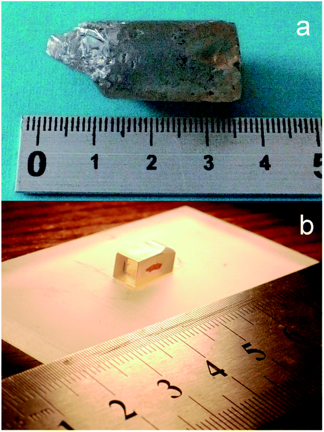 | ||
| Fig. 1 (a) Photo of as-grown LiGaS2 crystal boule, (b) polished LiGaS2 plate used in the present XPS and XES measurements. | ||
3 Computational method
Lithium thiogallate LiGaS2 (LGS) crystalizes in a non-centrosymmetric structure with space group Pna21. The orthorhombic system was simulated based on experimental lattice parameters a = 6.5133 Å, b = 7.8629 Å, c = 6.2175 Å.10 As shown in Fig. 2, one Ga atom connects with four S atoms to create a GaS4 tetrahedron. Meanwhile, the Li atoms are situated in cavities formed by Ga–S bonds.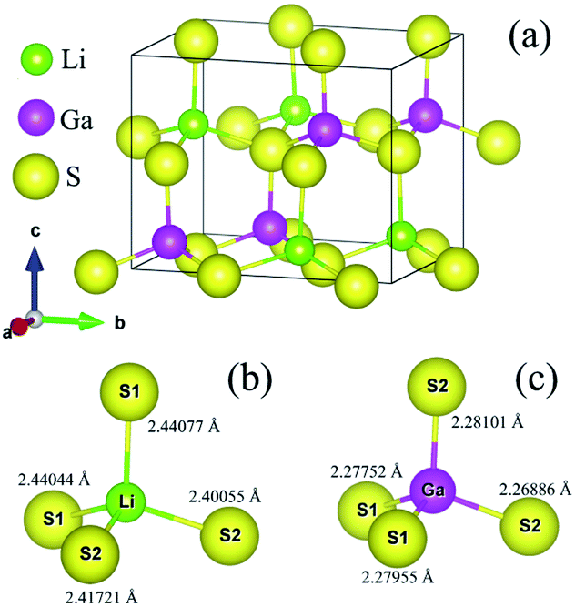 | ||
| Fig. 2 (a) Orthorhombic structure of LiGaS2, and distorted (b) LiS4 and (c) GaS4 tetrahedra in the LiGaS2 crystal. | ||
The electronic structure calculation for LiGaS2 crystals was performed by applying the augmented plane wave plus local-orbital (APW+lo) method43,44 as implemented in the WIEN2k package.45 The Muffin-Tin (MT) model was used to reproduce the system’s full potential without shape approximations, where the MT radius for Li, Ga, and S was 2.09 (a.u), 2.29 (a.u) and 1.97 (a.u), respectively. The expansion of the wavefunction, within a Brillouin zone of 3000 k-points, was limited by the maximum angular momentum lmax = 10, and RMTminkmax = 8. The Fourier expansion of charge density was carried out until Gmax = 14 (a.u.)−1. The exchange–correlation potential was modeled by both traditional GGA-PBE method46 and a TB-mBJ functional.47,48 The Coulomb repulsion of strongly correlated Ga-3d states was treated by the Hubbard technique.49,50 The Hubbard parameter U = 0.515 Ry was applied for 3d states of Ga, because this U value was proven to be suitable for systems containing the Ga element.26 The convergence of a self-consistent process was controlled by setting the charge density difference to be less than 10−4 Ry.
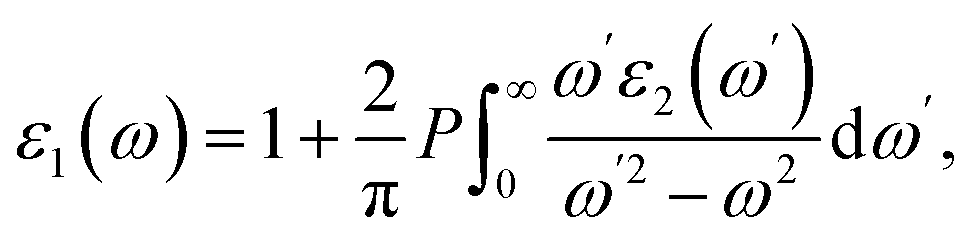
The optical properties of the LiGaS2 crystal were calculated based on the dielectric function ε(ω) = ε1(ω) + ε2(ω)51 which in turn depends on the unit-cell volume V, the crystal momentum k, spin σ, and the eigenvalue energy Ekn of the wave function |knp〉. Applying the Kramers–Kronig relations,52 ε2(ω), and ε1(ω) can be calculated as follows:53
 | (1) |
 | (2) |
4 Results and discussion
4.1 XPS studies of the LiGaS2 crystal
The survey XPS spectrum of the pristine surface of the LiGaS2 crystal (Fig. 3) reveals only the presence of the constituent elements and, in addition, signals associated with adsorbed oxygen- and hydrocarbon-containing species. The binding energy value of the C 1s line is impossible to evaluate precisely because it superimposes the Auger Ga L3M23M45 line in the LiGaS2 crystal; however, its presence is evidenced through the existence of the Auger C KLL line when measuring the pristine crystal surface (Fig. 3). The binding energy of the O 1s line in the case of the pristine LiGaS2 crystal surface (the spectrum is not presented here) gives the value of 531.8 ± 0.1 eV, corresponding exclusively to oxygen adsorbed from the laboratory air.54 Treatment of the pristine surface with middle-energy (3 keV) Ar+ ions (5 min duration, ion current density was set to be equal to about 17 mA cm−2 as we used in the case of the related chalcogenide compounds, LiGaSe2 (ref. 26) and LiGa0.5In0.5Se2 (ref. 28)), leads to almost complete elimination of adsorbed oxygen- and hydrocarbon-containing species. These facts show the high optical quality and low-hygroscopicity of the LiGaS2 crystal surface. Previously, such peculiarities have been found to be characteristic of the related selenides LiGaSe2 (ref. 26) and LiGa0.5In0.5Se2.28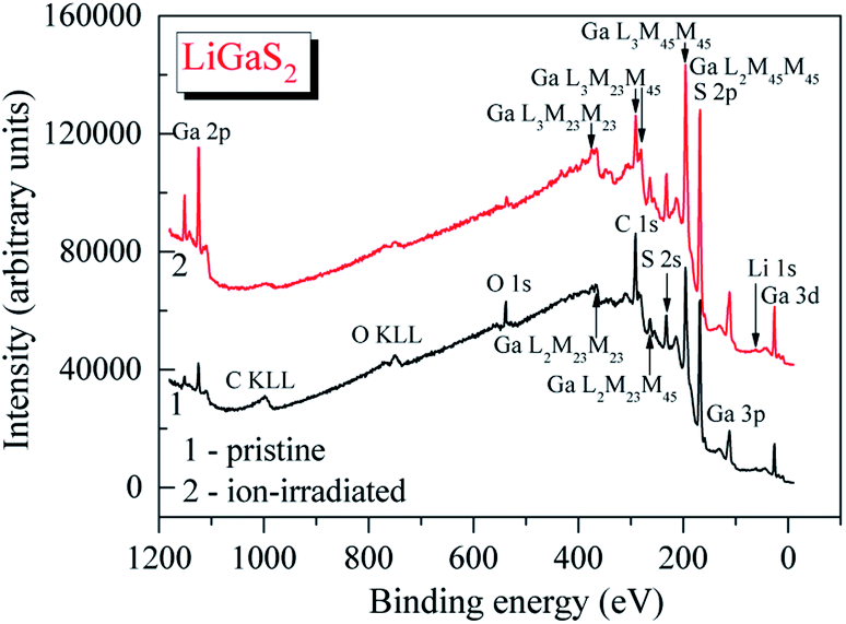 | ||
| Fig. 3 Survey XPS spectra of (1) pristine and (2) Ar+-ion irradiated surfaces of the LiGaS2 crystal. | ||
Detailed XPS measurements of the most important core-level spectra associated with lithium, gallium and sulfur atoms (Fig. 4) indicate that the 3 keV Ar+ ion-treatment does not lead to visible changes in the shapes of the XPS spectra or the binding energy values (Table 1). We do not see the formation of new fine-structure peculiarities in the XPS valence-band spectra in such a case (Fig. 5). Therefore, like in the case of selenides LiGaSe2,26 and LiGa0.5In0.5Se2,28 the LiGaS2 crystal also reveals the high chemical stability. In the LiGaS2 crystal, the XPS S 2p core-level spectrum superimposes the Auger Ga L2M45M45 line, as Fig. 4(c) demonstrates.
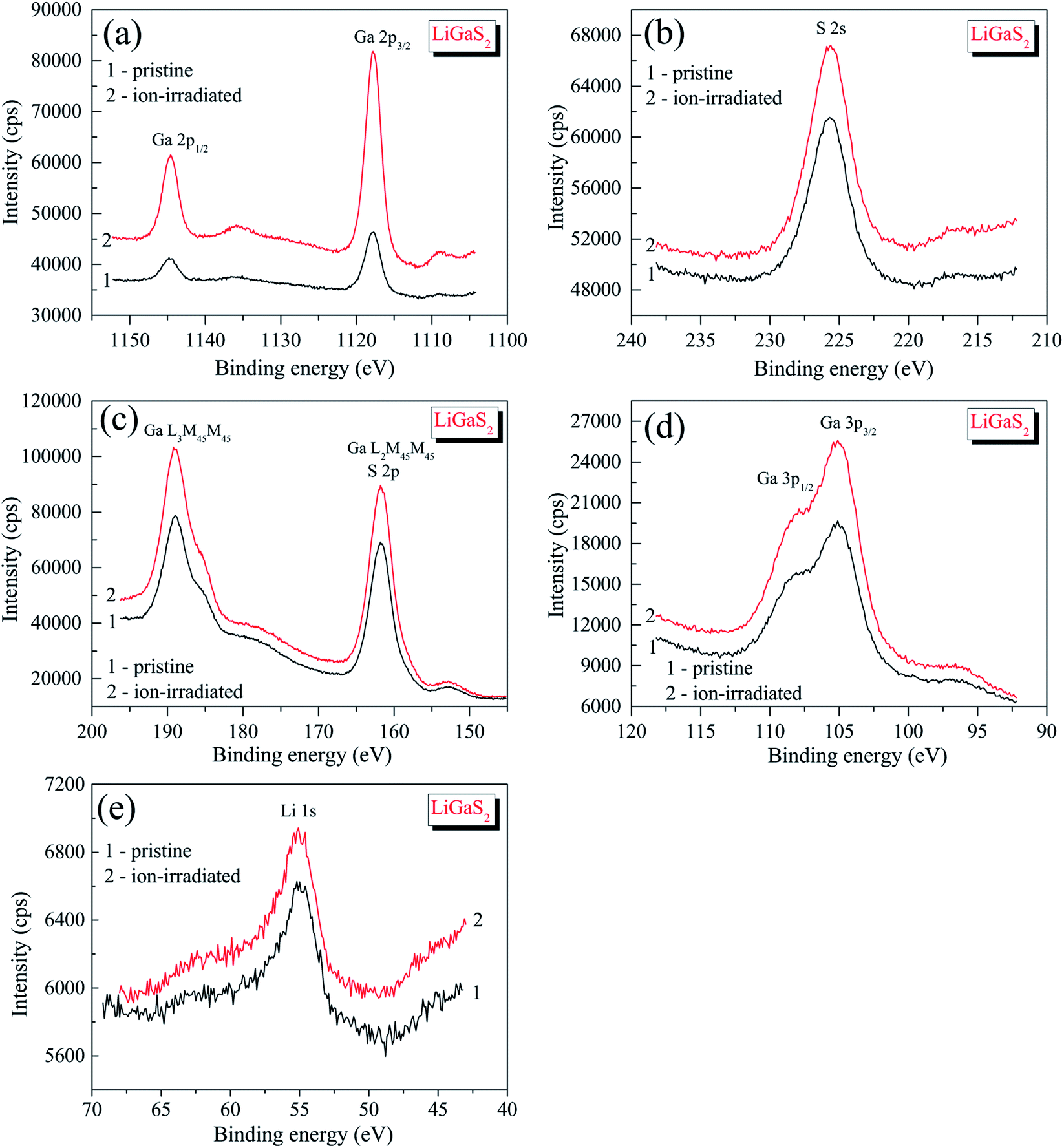 | ||
| Fig. 4 Detailed XPS core-level spectra of (1) pristine and (2) Ar+-ion irradiated surfaces of the LiGaS2 crystal: (a) Ga 2p, (b) S 2s, (c) S 2p (and Auger Ga L3M45M45 and Ga L2M45M45 lines), (d) Ga 3p, and (e) Li 1s. | ||
 | ||
| Fig. 5 XPS valence-band spectra of (1) pristine and (2) Ar+-ion irradiated surfaces of the LiGaS2 crystal. | ||
It is worth mentioning that XPS is recognized as an experimental technique that is very sensitive to peculiarities in the chemical bonding in solids.40,54 However, it is also very sensitive to surface charge effects and calibration methods. Therefore, it is beneficial to ensure that XPS measurements are performed with one instrument and the same experimental conditions are used. Previously, we measured XPS spectra of the related selenide, LiGaSe2 (ref. 26), and derived a binding energy of 1117.34 ± 0.05 eV for Ga 2p3/2 core-level spectrum. Since the experiments in ref. 26 were performed under similar experimental conditions as compared to those used in the present work, comparison of the above binding energy value with that derived for the Ga 2p3/2 core-level of LiGaS2 (1117.88 ± 0.05 eV; Table 1) allows us to conclude that the ionic component of the Ga–X bonds (X = S, Se) decreases when in the LiGaX2, the chalcogenide sulfur is substituted by selenium. The comparison of the ionic component of the Li–X bonds (X = S, Se) in LiGaX2 can not be made because the Li 1s spectrum superimposes the Se 3d spectrum in selenide LiGaSe2.26
4.2 Electronic properties of LiGaS2
The band gap Eg is one of the key factors to define the laser damage resistance of LiGaS2. However, it has not been well reproduced by previous theoretical studies of this sulfide. Due to the discontinuity of the exchange–correlation potential or the over-delocalization of the valence band (VB) in the GGA/LDA calculation, the LiGaS2 band gap is about 1 eV smaller than the experimental data.10,21–24,55,56 The experimental band gap of LiGaS2 can be 3.93 eV, 4.03 eV, and 4.15 eV, depending on temperature and the thickness of sample.10,57,58 To achieve consistency between theory and experiment, the atomic positions in LiGaS2 were taken from an experimental study which reveals an LiGaS2 band gap of 4.15 eV,10 the strongly correlated electrons of Ga d-orbitals were treated by Hubbard U parameter as it is reported to improve the Eg by about 0.2 eV,21,23 and correction is added to the exchange effect in the TB-mBJ method.47,48,59,60As can be seen from the data reported in Table 2, the LiGaS2 band gap obtained by PBE-GGA and PBE-GGA+U are 3.259 eV, and 3.202 eV, respectively. These values are just slightly different from previous theoretical studies, and the introduction of the Hubbard parameter U does not lead to a significant improvement of the LiGaS2 band structure, as shown in Fig. 6. The TB-mBJ method results in a remarkable shift of conduction band (CB) to an upper energy level, Fig. 6, giving a LiGaS2 band gap of 4.566 eV, which is about 0.4 eV bigger than the experimental data.10 Meanwhile, the TB-mBJ+U method reduces the difference between theoretical and experimental band gaps down to 0.27 eV. The TB-mBJ+U band structure of LiGaS2 is presented in Fig. 7. As both VB maximum and CB minimum are located at Γ-point, LiGaS2 is also a direct band gap semiconductor like other members in the family LiMX2 (M = In, Ga, X = S, Se).10 This result is consistent with experimental studies.58 The band dispersion near the valence region is mainly flat implying rather high effective mass, and peculiarities of the bonding nature in LiGaS2. Subsequently, the hopping of particles between different regions in real space is expected to be inhibited.
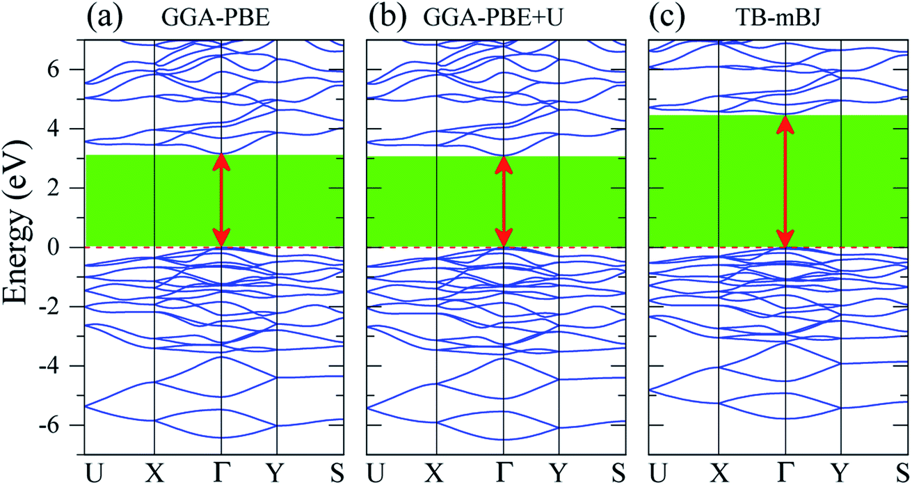 | ||
| Fig. 6 Band structure of LiGaS2 calculated by (a) GGA-PBE, (b) GGA-PBE+U, and (c) TB-mBJ methods (the Fermi level is set to zero). | ||
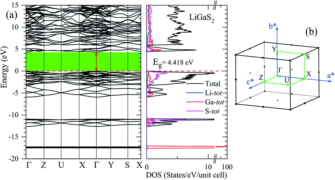 | ||
| Fig. 7 (a) TB-mBJ+U band structure and DOS of LiGaS2 along the high-symmetric direction in (b) the Brillouin zone. | ||
In previous work, the TDOS calculated by GAA/LDA fails in describing the d-orbital of Ga which is at very low density.18 The d-orbital of Ga as well as the whole VB is shifted to a higher energy level, and therefore, the calculated band gap is significantly reduced.22 The reliability of the TB-mBJ+U method is confirmed by comparing the TDOS with the XPS spectrum of the VB in the LiGaS2 crystal (Fig. 8). It can be seen that the TB-mBJ+U method is very good with respect to reproducing the XPS spectrum with main peaks in the vicinity of −17.6 eV, −13 to −11 eV, −6 to −4 eV, and −3 to 0 eV. The highest part of the LiGaS2 VB is mainly constructed by the hybridization of s/p-orbitals from the Li, Ga, and S elements. The strong hybridization of Li-2s and S-3p orbitals reveals the covalent nature of the Li–S bonds. Meanwhile, the admixture of S-3p and Li-2p orbitals results in a sharp increase of DOS at the VB maximum. While the d-orbitals of Ga are the only contributors to VB with the lowest part at −17.5 eV, the unoccupied CB is formed by hybridization of Li-2p, Ga-4s, and S-3p orbitals.
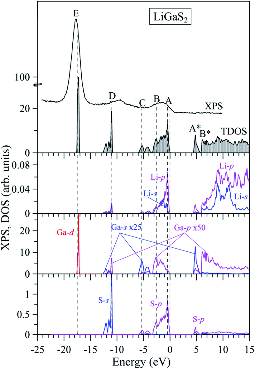 | ||
| Fig. 8 Total and partial DOS of LiGaS2 compound (obtained by the TB-mBJ+U method) in comparison with the XPS spectrum. The DOS of Ga-s, and Ga-p are zoomed-in by 25, and 50 times, respectively. The VB maximum was set to be at the Fermi level, while the energy level of the XPS spectrum was also shifted to match the total DOS. | ||
Regarding the occupancy of the LiGaS2 VB by S-3p and Ga-4p states, the substantial contributors in the valence-band region, as Fig. 9 presents, show that the above theoretical predictions are reasonably supported by the data of the present XES measurements. Fig. 9 presents the comparison results, on a general energy scale, of the XES S Kβ1,3 and Ga Kβ2 spectra, providing the energy distribution of the S 3p and Se 4p states in LiGaS2, respectively, with the XPS VB spectrum. From Fig. 9, it is clear that the main maximum of the S Kβ1,3 band (S-3p states) is detected at the top of the XPS VB spectrum (peculiarity A), while the main maximum of the XES Ga Kβ2 band (Ga-4p states) is positioned near peculiarity B of the XPS spectrum (cf. Fig. 8 and 9). As can be seen from Fig. 8, the theoretical data also predict substantial input from the Ga-4s states at the bottom of the LiGaS2 VB, while minor contributions of Li-2s, 2p states contribute to the upper portion. However, the available ability of our group does not allow experimental measurements of those states in the LiGaS2 crystal.
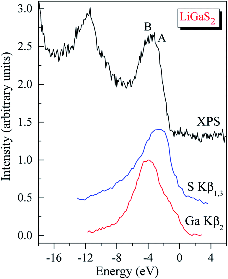 | ||
| Fig. 9 XPS valence-band spectrum of the LiGaS2 crystal matched on a common energy scale with the XES S Kβ1,3 and Ga Kβ2 bands. | ||
One of the emission maxima in LiGaS2 was observed at 5 eV,58 this is exactly the band-to-band transition between peak A in the VB maximum and the highest peak A* in the CB lowest peak, as shown in Fig. 8. The remaining extrema in the spectra of pink, blue, and violet photoluminescence are at lower intensity and they are observed at 3.4 eV, 3.94 eV, 2.9 eV, 2.74 eV, 2.98 eV, and 3.28 eV.58 The reduction in emission energies may arise from experimental factors including temperature, defects, self-trapped exciton.61,62 In the framework of theoretical calculations, this reduction may also originate from the low intensity of bands near the band gap, as shown in Fig. 8. Since the photoluminescence originates from absorption and recombination processes, the optical properties of LiGaS2, including dielectric function, and absorption rate are calculated in the next paragraph.
4.3 Optical properties of LiGaS2
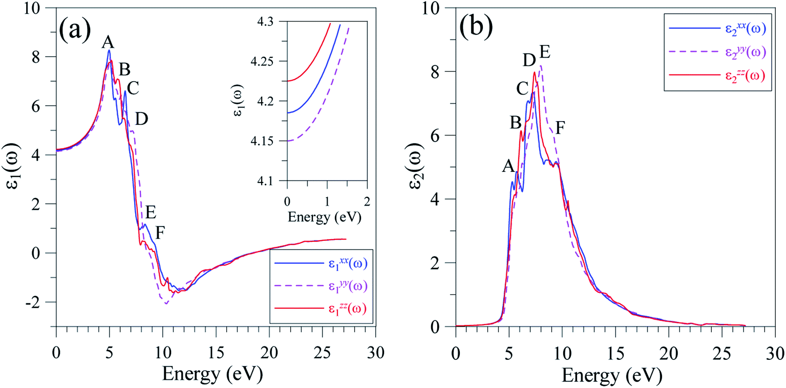
The reliable TB-mBJ+U electronic structure allows for the study of the dielectric function of LiGaS2 that is formed as a result of intra-band and inter-band transitions. As the LiGaS2 is a direct semiconductor, the indirect inter-band transition, which arises from phonon-scattering, is negligible.63–65The ε1(ω) spectrum of LiGaS2, as shown in Fig. 10(a), is characterized with main extrema A, B, C, D, E, and F in the vicinities of 4 eV, 5 eV, 5.5 eV, 6.5 eV, 7.5 eV, and 9 eV, respectively. The static values of ε1(0) are almost the same (ε1xx(0) = 4.185, ε1yy(0) = 4.150, ε1zz(0) = 4.225). It can be seen in Fig. 10(a), that LiGaS2 possesses high reflectivity for photons with energy of 3–6.5 eV. The polarization of dielectric function is strong in the energy level range 4–11 eV, within this range (ε1xx(0) is slightly higher than (ε1yy(0), and (ε1zz(0). The damping of the electro-magnetic wave occurs at about 9 eV where ε1(ω) becomes negative. At energy levels higher than 13 eV, ε1(ω) is almost isotropic, and slightly increases to a positive value near zero. The imaginary part of the dielectric function (Fig. 10(b)) is only anisotropic in the energy range 6–11 eV. The extrema A, B, C, D, E, and F occur near energy levels of 5.5 eV, 6 eV, 6.5 eV, 7 eV, 8, and 9 eV, respectively. Analyzing Fig. 8 and 10, it is obvious that the extrema in the ε2(ω) spectra correspond to the inter-band transitions from S-3p/Li-2s/Li-2p/Ga-4s states to Ga-4s/Ga-4p/Li-2p/Li-2s states. The inter-band transition happens only from energy levels of −4 to 0 eV in the VB to energy levels of 4–6 eV in the CB. It is also shown that the value of ε2xx(ω) is always lower than those of ε2yy(ω), and ε2zz(ω) which are close to each other.
 | ||
| Fig. 10 Polarization of (a) ε1(ω), and (b) ε2(ω) spectra along x-, y-, and z-directions in the LiGaS2 crystal. | ||
It is well-known that the imaginary part of the dielectric function is proportional to the joint density of states,66,67 which is relative to the power of emission. As ε2(ω) reaches its extrema at 5.5 eV, 6 eV, 6.5 eV, 7 eV, 8, and 9 eV, it is expected that the emission is from a high intensity of photons in these energy ranges. However, previous measurements58 show only one theoretical maximum at 5 eV. Our theoretical results indicate a need to measure the emission in LiGaS2 at higher energy levels. Meanwhile, in the framework of theoretical calculations, some aspects of the photoluminescence can be revealed via the absorption spectrum α(ω), which was calculated by the TB-mBJ+U method and is presented in Fig. 11.
 | ||
| Fig. 11 Polarization of the absorption spectrum α(ω) along x-, y-, and z-directions in the LiGaS2 crystal. | ||
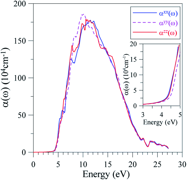
For the energy range 0.1–3.9 eV (0.32–11.6 μm), the LiGaS2 compound is reported to be nearly transparent.58 This experimental result is reasonable because the electromagnetic wave absorption of LiGaS2 in this energy level is very low. However, the α(ω) neatly maintains at 104 cm−1 which results in pink, blue, and violet emission with main extrema at 2.74 eV, 2.9 eV, 2.98 eV, 3.28 eV, 3.38 eV, 3.4 eV, and 3.94 eV.63
As shown in Fig. 11, the optical absorption edge is observed near 4.4 eV. The first extremum of α(ω) is near 5 eV, which is also the highest intensity of emission observed in previous work.62 The emission at higher energy levels has not been available, however it can be seen that LiGaS2 single crystal intensively absorbs propagating electro-magnetic waves with photon energies in the range of 7–17 eV, where the α(ω) is in the order of magnitude of 106 cm−1. At energy ranges of 8–11 eV, the absorption αyy(ω) is slightly higher than αxx(ω), and αzz(ω), whose intensities are almost the same. At energy levels higher than 17 eV, there is a sharp decrease of absorption in LiGaS2, and negligible polarization.
Since the polarization of absorption α(ω) is significant at high energy levels, it is expected that the intensity of photoluminescence in LiGaS2 also depends on different directions. It is necessary to note that the emission at high energy level results in a high refractive index.68 Therefore, the photoluminescence is actually observed to be best preserved in the normal direction.69 On the other hand, the reflected emission can cause attenuation of photoluminescence.69 Therefore, the refractive index n(ω) and extinction coefficient k(ω) were calculated and are presented in Fig. 12.
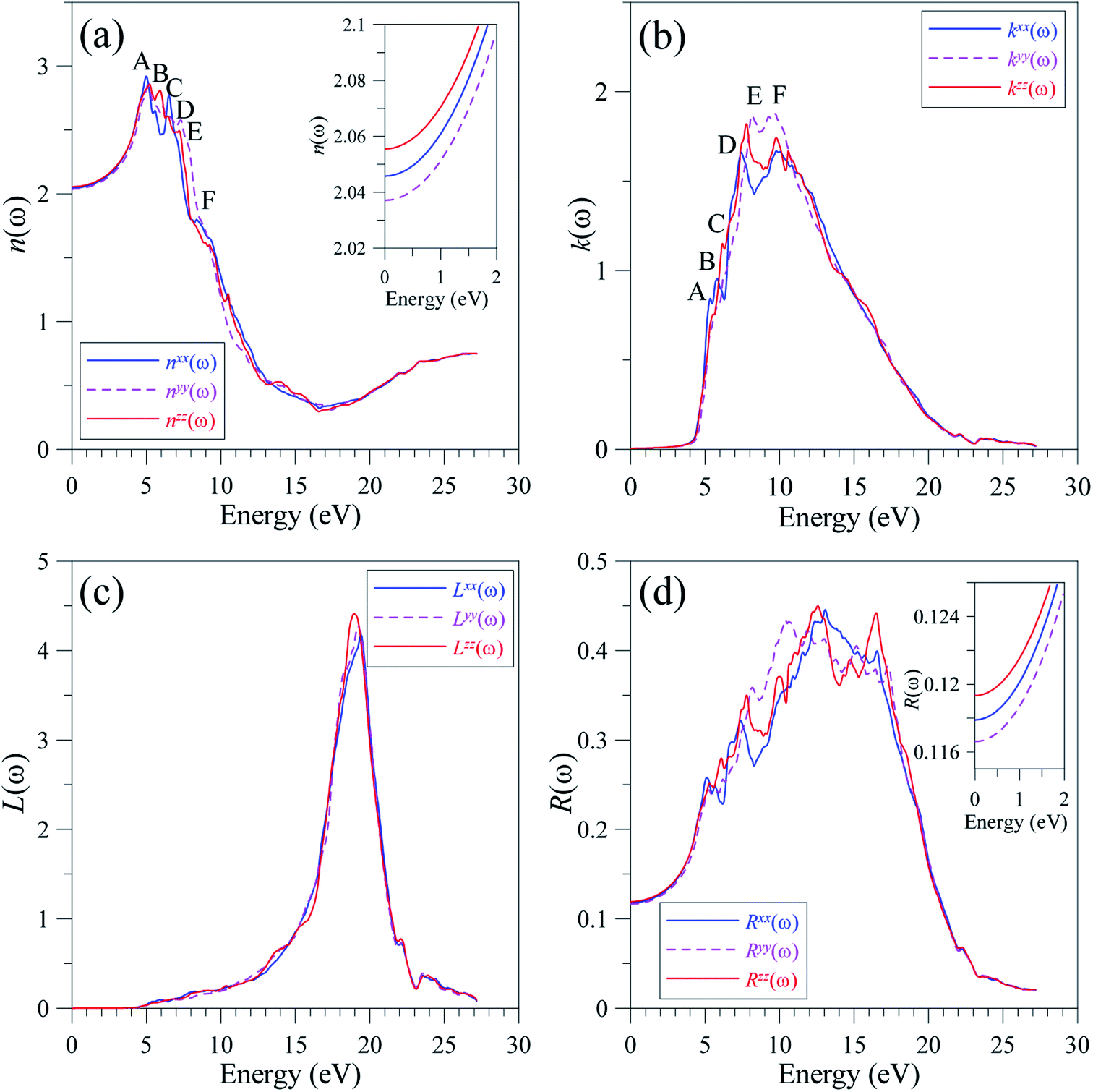 | ||
| Fig. 12 Polarization of (a) refractive index n(ω), (b) extinction coefficient k(ω), (c) electron energy-loss spectrum L(ω), and (d) optical reflectivity R(ω) along x-, y-, and z-directions in the LiGaS2 crystal. | ||
At equilibrium, the refractive indices n(ω) along x-, y-, and z-directions in the LiGaS2 crystal are very close to each other. The difference in the values of n(ω) remains minor in the transparent region of 0–3.9 eV.58 The polarization becomes strong in the energy range of 4.4–13 eV, where nxx(ω) > nzz(ω) > nyy(ω) (Fig. 12(a)). In the energy range of 5–8 eV, n(ω) reaches its extrema in the vicinity of 5, 6, 6.2, 7, 7.2, and 8 eV, where LiGaS2 exhibits its best phase-matching as the birefringence is most remarkable.70 As the conditions for phase-matching are met, the constructive interference is expected to occur leading to a high intensity field. Generally, the intensities of k(ω) along the three crystal directions of LiGaS2 are nearly the same, Fig. 12(b). However, there is a remarkable shift of kyy(ω) to higher energy levels within the energy range of 7–11 eV. At the energy range of 5–17 eV, the attenuation of the propagating wave is at a high rate as the extinction coefficient k(ω) is as high as 1–2. This is also the energy range where the absorption rate α(ω) is the highest. So, the extinction coefficient k(ω) is well proportional to α(ω). Due to the absorption process, the energy-loss L(ω) is partly caused by thermalization during the inter-band transition. As shown in Fig. 12(c), the energy loss becomes significant in the energy range of 5–18 eV, then it sharply increases to the highest values of about 4.5 in the narrow energy range of 18–20 eV. The plasma frequency is expected to be at 19 eV, signifying a plasma frequency of about 4594 THz. This is also the energy level of strong polarization, where Lzz(ω) is obviously higher than Lxx(ω), and Lyy(ω). The reflectivity spectrum R(ω) extends to 22 eV with strong polarization at the extrema in the vicinity of 5, 6, 7, 10, 12, and 16 eV (Fig. 12(d)). The static values of the reflectivity spectrum R(ω) are as follows: (Rxx(ω) = 11.79%, Ryy(ω) = 11.661%, Rzz(ω) = 11.933%).
5 Conclusion
The electronic and optical properties of lithium thiogallate (LiGaS2) were studied by XPS and XES measurements, and DFT calculations. The theoretical calculation was performed using the GGA, and TB-mBJ methods where the effect of the Coulomb repulsion was also considered by introducing the Hubbard parameter U into the GGA+U, and TB-mBJ+U methods.Despite the fact that the LiGaS2 crystal structure was modeled based on experimental data, both GGA and LDA methods reproduce a band gap that is about 1 eV smaller than the experimental measurements. The improvement of exchange–correlation potential via the TB-mBJ method leads to a band gap of about 0.4 eV higher than the experimental data. The Hubbard parameter in the TB-mBJ+U method plays an important role in reducing the difference between theoretical and experimental results to 0.27 eV.
The nature of the band-to-band transition, which is relative to the photoluminescence in LiGaS2, was studied by analyzing the DOS, TDOS, and XPS spectra. Both the TB-mBJ+U method and XPS spectrum separate the valance band of LiGaS2 into the lowest part at −17.6 eV (mainly contributed to by the d-orbitals of Ga); the middle part at −13 to −11 eV (donated by s/p-orbitals from Li, Ga, and S elements); and the highest part at −6 to 0 eV (donated by s/p-orbitals of Li, and S elements). Meanwhile, the Li-2p, Ga-4s, and S-3p orbitals provide the major contribution to the CB. Regarding the occupancy of the LiGaS2 VB by S-3p and Ga-4p states, the above theoretical predictions are reasonably supported by data of the present XES and XPS measurements when comparing them on the general energy scale of the XES S Kβ1,3 and Ga Kβ2 spectra bringing the energy distribution of S 3p an Se 4p states with the XPS VB spectrum. Furthermore, the XPS data indicate the low hygroscopicity of the LiGaS2 crystal surface. The ionic component of the Ga–X bonds (X = S, Se) decreases when in the LiGaX2 chalcogenide sulfur is substituted by selenium.
LiGaS2 possesses high reflectivity for photons with energies 3–6.5 eV, where the ε1(ω) spectrum reaches its extrema. The polarization of dielectric function is strong in the energy level range 4–11 eV. The theoretical spectra of LiGaS2 dielectric function ε(ω) confirm the band-to-band transition relating to the photoluminescence of pink, blue, and violet spectra, where the emission is observed at energy levels lower than 5 eV. As ε2xx(ω) reaches its extremum beyond 5 eV, it is recommended to measure the emission of LiGaS2 at higher energy levels. The transparency of LiGaS2 in the energy range 0.1–3.9 eV (0.32–11.6 μm) is confirmed by the current theoretical results. The LiGaS2 single crystal is predicted to intensively absorb photons with energies of 7–17 eV, with the absorption rate α(ω) is in the order of magnitude of 106 cm−1, where the polarization is remarkable in such a case.
LiGaS2 can exhibit constructive interference with high intensity fields at 5, 6, 6.2, 7, 7.2, and 8 eV, where the birefringence is most remarkable (nxx(ω) > nzz(ω) > nyy(ω)). The extinction coefficient k(ω) is highest in the energy range of 5–17 eV. The loss energy L(ω) reaches the highest value near 19 eV, signifying a plasma frequency of about 4594 THz. The reflectivity spectrum R(ω) is at high intensity (0.1–0.5) in the energy range of 0–20 eV.
Conflicts of interest
There are no conflicts to declare.Acknowledgements
This research is funded by the Vietnam National Foundation for Science and Technology Development (NAFOSTED) under grant number 103.01-2018.334. This work was partly done on state assignment of IGM SB RAS, Ministry of Science and Higher Education of the Russian Federation.References
- J. Kim and T. Hughbanks, Inorg. Chem., 2000, 39, 3092–3097 CrossRef CAS PubMed.
- B. F. Levine, Phys. Rev. B: Solid State, 1973, 7, 2600–2626 CrossRef CAS.
- G. D. Boyd, E. Buehler and F. G. Storz, Appl. Phys. Lett., 1971, 18, 301–304 CrossRef CAS.
- G. Boyd, H. Kasper, J. McFee and F. Storz, IEEE J. Quantum Electron., 1972, 8, 900–908 CrossRef CAS.
- D. S. Chemla, P. J. Kupecek, D. S. Robertson and R. C. Smith, Opt. Commun., 1971, 3, 29–31 CrossRef CAS.
- S. Fossier, S. SalaÃijn, J. Mangin, O. Bidault, I. ThÃľnot, J.-J. Zondy, W. Chen, F. Rotermund, V. Petrov, P. Petrov, J. Henningsen, A. Yelisseyev, L. Isaenko, S. Lobanov, O. Balachninaite, G. Slekys and V. Sirutkaitis, J. Opt. Soc. Am. B, 2004, 21, 1981–2007 CrossRef CAS.
- L. Isaenko, A. Yelisseyev, S. Lobanov, P. Krinitsin, V. Petrov and J. J. Zondy, J. Non-Cryst. Solids, 2006, 352, 2439–2443 CrossRef CAS.
- V. Petrov, J.-J. Zondy, O. Bidault, L. Isaenko, V. Vedenyapin, A. Yelisseyev, W. Chen, A. Tyazhev, S. Lobanov, G. Marchev and D. Kolker, J. Opt. Soc. Am. B, 2010, 27, 1902–1927 CrossRef CAS.
- L. Isaenko, I. Vasilyeva, A. Yelisseyev, S. Lobanov, V. Malakhov, L. Dovlitova, J. J. Zondy and I. Kavun, J. Cryst. Growth, 2000, 218, 313–322 CrossRef CAS.
- L. Isaenko, A. Yelisseyev, S. Lobanov, A. Titov, V. Petrov, J.-J. Zondy, P. Krinitsin, A. Merkulov, V. Vedenyapin and J. Smirnova, Cryst. Res. Technol., 2003, 38, 379–387 CrossRef CAS.
- V. Petrov, Prog. Quantum Electron., 2015, 42, 1–106 CrossRef.
- L. Isaenko, I. Vasilyeva, A. Merkulov, A. Yelisseyev and S. Lobanov, J. Cryst. Growth, 2005, 275, 217–223 CrossRef CAS.
- K. Kuriyama and T. Nozaki, J. Appl. Phys., 1981, 52, 6441–6443 CrossRef CAS.
- J. Leal-Gonzalez, S. A. Melibary and A. J. Smith, Acta Crystallogr., Sect. C: Cryst. Struct. Commun., 1990, 46, 2017–2019 CrossRef.
- A. Tyazhev, V. Vedenyapin, G. Marchev, L. Isaenko, D. Kolker, S. Lobanov, V. Petrov, A. Yelisseyev, M. Starikova and J.-J. Zondy, Opt. Mater., 2013, 35, 1612–1615 CrossRef CAS.
- V. Petrov, A. Yelisseyev, L. Isaenko, S. Lobanov, A. Titov and J. J. Zondy, Appl. Phys. B: Lasers Opt., 2004, 78, 543–546 CrossRef CAS.
- K. Kaneshima, N. Ishii, K. Takeuchi and J. Itatani, Opt. Express, 2016, 24, 8660–8665 CrossRef CAS PubMed.
- C. T. Chen, L. Bai, Z. Z. Wang and R. K. Li, J. Cryst. Growth, 2006, 292, 169–178 CrossRef CAS.
- F. Meyers, J. L. Bredas and J. Zyss, J. Am. Chem. Soc., 1992, 114, 2914–2921 CrossRef CAS.
- A. P. Yelisseyev, L. I. Isaenko, P. Krinitsin, F. Liang, A. A. Goloshumova, D. Y. Naumov and Z. Lin, Inorg. Chem., 2016, 55, 8672–8680 CrossRef CAS PubMed.
- V. V. Atuchin, L. I. Isaenko, V. G. Kesler, S. Lobanov, H. Huang and Z. S. Lin, Solid State Commun., 2009, 149, 572–575 CrossRef CAS.
- T.-h. Ma, C.-h. Yang, Y. Xie, L. Sun, W.-q. Lv, R. Wang and Y.-l. Ren, Phys. B, 2010, 405, 363–368 CrossRef CAS.
- A. H. Reshak, S. Auluck, I. V. Kityk, Y. Al-Douri, R. Khenata and A. Bouhemadou, Appl. Phys. A: Mater. Sci. Process., 2009, 94, 315–320 CrossRef CAS.
- L.-H. Li, J.-Q. Li and L.-M. Wu, J. Solid State Chem., 2008, 181, 2462–2468 CrossRef CAS.
- N. Guechi, A. Bouhemadou, I. Benaisti, S. Bin-Omran, R. Khenata and Y. Al-Douri, J. Alloys Compd., 2020, 815, 152384 CrossRef CAS.
- A. A. Lavrentyev, B. V. Gabrelian, V. T. Vu, L. N. Ananchenko, L. I. Isaenko, A. P. Yelisseyev and O. Y. Khyzhun, Opt. Mater., 2017, 66, 149–159 CrossRef CAS.
- A. A. Lavrentyev, B. V. Gabrelian, V. T. Vu, L. N. Ananchenko, L. I. Isaenko, A. Yelisseyev, P. G. Krinitsin and O. Y. Khyzhun, Phys. B, 2016, 501, 74–83 CrossRef CAS.
- A. A. Lavrentyev, B. V. Gabrelian, T. V. Vu, L. I. Isaenko, A. P. Yelisseyev and O. Y. Khyzhun, Opt. Mater., 2018, 80, 12–21 CrossRef CAS.
- A. H. Reshak, Z. A. Alahmed and J. Bila, J. Alloys Compd., 2019, 771, 607–613 CrossRef CAS.
- N. B. Stambouli, T. Ouahrani, M. Badawi, A. H. Reshak and S. Azizi, J. Alloys Compd., 2019, 803, 1127–1135 CrossRef CAS.
- S. N. Rashkeev and W. R. L. Lambrecht, Appl. Phys. Lett., 2000, 77, 190–192 CrossRef CAS.
- A. Lavrentyev, B. Gabrelian, V. Vu, P. Shkumat, V. Ocheretova, O. Parasyuk and O. Khyzhun, Opt. Mater., 2015, 47, 435–444 CrossRef CAS.
- T. V. Vu, A. A. Lavrentyev, B. V. Gabrelian, K. D. Pham, C. V. Nguyen, K. C. Tran, H. L. Luong, M. Batouche, O. V. Parasyuk and O. Y. Khyzhun, J. Electron. Mater., 2019, 48, 705–715 CrossRef CAS.
- T. Djaafri, H. Bouafia, B. Sahli, B. Djebour, Ş. Uğur, G. Uğur and H. Moussa, J. Magn. Magn. Mater., 2020, 493, 165730 CrossRef CAS.
- T. V. Vu, A. A. Lavrentyev, B. V. Gabrelian, H. D. Tong, V. A. Tkach, O. V. Parasyuk and O. Y. Khyzhun, Opt. Mater., 2019, 96, 109296 CrossRef CAS.
- T. V. Vu, A. A. Lavrentyev, B. V. Gabrelian, H. D. Tong, V. A. Tkach, O. V. Parasyuk and O. Y. Khyzhun, Optik, 2020, 202, 163709 CrossRef.
- B. V. Gabrelian, A. A. Lavrentyev, T. V. Vu, V. A. Tkach, O. V. Marchuk, K. F. Kalmykova, L. N. Ananchenko, O. V. Parasyuk and O. Y. Khyzhun, Chem. Phys., 2020, 536, 110821 CrossRef CAS.
- T. V. Vu, A. A. Lavrentyev, B. V. Gabrelian, V. A. Tkach, K. D. Pham, O. V. Marchuk, O. V. Parasyuk and O. Y. Khyzhun, Solid State Sci., 2020, 104, 106287 CrossRef CAS.
- A. Y. Tarasova, L. I. Isaenko, V. G. Kesler, V. M. Pashkov, A. P. Yelisseyev, N. M. Denysyuk and O. Y. Khyzhun, J. Phys. Chem. Solids, 2012, 73, 674–682 CrossRef CAS.
- Practical Surface Analysis, ed. D. Briggs and P. M. Seach, John Willey & Sons Ltd., Chichester, 2nd edn, 1990, vol. 1: Auger and X-Ray Photoelectron Spectroscopy Search PubMed.
- O. Y. Khyzhun, V. V. Halyan, I. V. Danyliuk and I. A. Ivashchenko, J. Mater. Sci.: Mater. Electron., 2016, 27, 3258–3264 CrossRef CAS.
- V. V. Halyan, O. Y. Khyzhun, I. A. Ivashchenko, A. H. Kevshyn, I. D. Olekseyuk, P. Tyshchenko, O. P. Vovk and Y. V. Bulik, Phys. B, 2018, 544, 10–16 CrossRef CAS.
- K. Schwarz, P. Blaha and G. K. H. Madsen, Comput. Phys. Commun., 2002, 147, 71–76 CrossRef.
- W. Kohn, A. D. Becke and R. G. Parr, J. Phys. Chem., 1996, 100, 12974–12980 CrossRef CAS.
- P. Blaha, K. Schwarz, G. K. H. Madsen, D. Kvasnicka, J. Luitz, R. Laskowski, F. Tran and L. D. Marks, WIEN2k, An Augmented Plane Wave + Local Orbitals Program for Calculating Crystal Properties, ed. Karlheinz Schwarz, Techn. Universität Wien, Austria, 2018 Search PubMed.
- J. P. Perdew, K. Burke and M. Ernzerhof, Phys. Rev. Lett., 1996, 77, 3865–3868 CrossRef CAS PubMed.
- D. Koller, F. Tran and P. Blaha, Phys. Rev. B: Condens. Matter Mater. Phys., 2012, 85, 155109 CrossRef.
- F. Tran and P. Blaha, Phys. Rev. Lett., 2009, 102, 226401 CrossRef PubMed.
- V. I. Anisimov, I. V. Solovyev, M. A. Korotin, M. T. Czyżyk and G. A. Sawatzky, Phys. Rev. B: Condens. Matter Mater. Phys., 1993, 48, 16929–16934 CrossRef CAS PubMed.
- P. Novák, F. Boucher, P. Gressier, P. Blaha and K. Schwarz, Phys. Rev. B: Condens. Matter Mater. Phys., 2001, 63, 235114 CrossRef.
- F. Wooten, Optical Properties of Solids, Academic Press, New York, 1972 Search PubMed.
- C. Ambrosch-Draxl and J. O. Sofo, Comput. Phys. Commun., 2006, 175, 1–14 CrossRef CAS.
- T. V. Vu, A. A. Lavrentyev, B. V. Gabrelian, O. V. Parasyuk, V. A. Ocheretova and O. Y. Khyzhun, J. Alloys Compd., 2018, 732, 372–384 CrossRef CAS.
- O. Y. Khyzhun, V. L. Bekenev, V. V. Atuchin, E. N. Galashov and V. N. Shlegel, Mater. Chem. Phys., 2013, 140, 588–595 CrossRef CAS.
- A. J. Cohen, P. Mori-Sánchez and W. Yang, Phys. Rev. B: Condens. Matter Mater. Phys., 2008, 77, 115123 CrossRef.
- D. Mei, W. Yin, K. Feng, Z. Lin, L. Bai, J. Yao and Y. Wu, Inorg. Chem., 2012, 51, 1035–1040 CrossRef CAS PubMed.
- J. Aarik, H. Mändar, M. Kirm and L. Pung, Thin Solid Films, 2004, 466, 41–47 CrossRef CAS.
- A. P. Yelisseyev, M. K. Starikova, V. V. Korolev, L. I. Isaenko and S. I. Lobanov, J. Opt. Soc. Am. B, 2012, 29, 1003–1011 CrossRef CAS.
- H. Jiang, J. Chem. Phys., 2013, 138, 134115 CrossRef.
- A. D. Becke and E. R. Johnson, J. Chem. Phys., 2006, 124, 221101 CrossRef PubMed.
- L.-C. Tang, C.-S. Chang, L.-C. Tang and J. Y. Huang, J. Phys.: Condens. Matter, 2000, 12, 9129–9143 CrossRef CAS.
- R. T. Williams and K. S. Song, J. Phys. Chem. Solids, 1990, 51, 679–716 CrossRef CAS.
- S. Hüfner, R. Claessen, F. Reinert, T. Straub, V. N. Strocov and P. Steiner, J. Electron Spectrosc. Relat. Phenom., 1999, 100, 191–213 CrossRef.
- A. H. Reshak, S. Auluck and I. V. Kityk, J. Alloys Compd., 2009, 473, 20–24 CrossRef CAS.
- N. V. Smith, Phys. Rev. B: Solid State, 1971, 3, 1862–1878 CrossRef.
- S. K. O’Leary, J. Mater. Sci.: Mater. Electron., 2004, 15, 401–410 CrossRef.
- Handbook of Optical Constants of Solids, ed. E. D. Palik, Academic Press, 1985, vol. 1, p. 804 Search PubMed.
- D. D. Sell, H. C. Casey and K. W. Wecht, J. Appl. Phys., 1974, 45, 2650–2657 CrossRef CAS.
- L. Wang, N. M. Haegel and J. R. Lowney, Phys. Rev. B: Condens. Matter Mater. Phys., 1994, 49, 10976–10985 CrossRef CAS.
- C. Chen, Z. Lin and Z. Wang, Appl. Phys. B: Lasers Opt., 2005, 80, 1–25 CrossRef CAS.
| This journal is © The Royal Society of Chemistry 2020 |