
 Open Access Article
 This Open Access Article is licensed under a Creative Commons Attribution-Non Commercial 3.0 Unported Licence
Vertically stacked SnSe homojunctions and negative capacitance for fast low-power tunneling transistors†
Hong Li *a,
Jiakun Lianga,
Peipei Xua,
Jing Luob and
Fengbin Liua
*a,
Jiakun Lianga,
Peipei Xua,
Jing Luob and
Fengbin Liua
aCollege of Mechanical and Material Engineering, North China University of Technology, Beijing 100144, P. R. China. E-mail: lihong@ncut.edu.cn
bBeijing Research Institute of Automation for Machinery Industry, Beijing 100120, P. R. China
First published on 2nd June 2020
Abstract
The two-dimensional (2D) vertical van der Waals (vdW) stacked homojunction is an advantageous configuration for fast low-power tunneling field effect transistors (TFETs). We simulate the device performance of the sub-10 nm vertical SnSe homojunction TFETs with ab initio quantum transport calculations. The vertically stacked device configuration has an effect of decreasing leakage current when compared with its planar counterpart due to the interrupted carrier transport path by the broken connection. A subthreshold swing over four decades (SSave_4 dec) of 44.2–45.8 mV dec−1 and a drain current at SS = 60 mV dec−1 (I60) of 5–7 μA μm−1 are obtained for the optimal vertical SnSe homojunction TFET with Lg = 10 nm at a supply voltage of 0.5–0.74 V. In terms of the device's main figures of merit (i.e., on-state current, intrinsic delay time, and power delay product), the vertical SnSe TFETs and NCTFETs outperform the 2022 and 2028 targets of the International Technology Roadmap for Semiconductors requirements for low-power application (2013 version), respectively.
1 Introduction
A tunneling field effect transistor (TFET) is a competitive post-CMOS low-power (LP) switch for future nano-electronics because avoiding thermionic carrier injection produces sub-60 mV dec−1 subthreshold swings (SS).1–4 The main challenge in adopting TFETs for real application is the low on-state currents (Ion) despite the sharp minimum SS. The use of two-dimensional (2D) (instead of 3D) semiconductors (e.g., black phosphorene (BP), bismuthine, GeSe, and SnSe) as channel materials can effectively improve Ion to enable TFETs even for high-performance (HP) applications with a single channel material and a simple planar p–i–n device configuration.5–8 However, unacceptably high leakage currents (Ileak) for LP applications are also found at the ultrashort sub-10 nm size. The planar ML SnSe TFET is one example.5 To reduce Ileak, structural modifications that can produce an additional tunneling barrier are appreciated. The vertically stacked configuration, i.e., to overlap a top and a bottom layer vertically in the channel region, is one suggested structural modification to lower Ileak.9As the first discovered 2D material with anisotropic charge transport characters, monolayer (ML) and few-layers BP are expected as the potential channel materials for next-generation nano-electronics like transistors and have been extensively investigated in labs.10–13 However, the excellent semiconducting properties of 2D BP would rapidly lose upon exposure to ambient conditions, which would somehow ruin the original outstanding device performances. Though air-stable 2D BP devices are realized by protective layers14–16 and ambient thermal treatment,17 the increased cost would undoubtedly hamper future large-scaled applications. Therefore, exploring new 2D channels with both excellent electronic properties and high stability is crucial for the manufacturing process of future nano-electronics. As one of BP analogs, ML and few-layers SnSe have been synthesized in labs in recent years.18–20 Similar to ML BP, ML SnSe is low-toxic and possesses excellent electronic properties like anisotropic electronic, moderate near direct bandgap, and high carrier mobility.21–23 Moreover, 2D SnSe has good ambient stability22,24 and economic earth-abundance elements, which are another two advantages for practical future nano-electronics. Considering the high current of the planar ML SnSe TFET and the above benefits, it's meaningful to find out whether the vertically stacked SnSe homojunction, which is much less studied than the planar configuration, could enable the SnSe TFET as fast LP device in regard to the International Technology Roadmap for Semiconductors (ITRS) requirements (2013 version). Besides, to find out whether the negative capacitance effect could improve the device performances evidently is also a meaningful issue.
In this paper, we investigate the device performances of the sub-10 nm vertical SnSe homojunction TFETs with ab initio quantum transport calculations. A sub-thermionic SS over four decades (SSave_4 dec) of 44.2–45.8 mV dec−1 and a drain current at SS = 60 mV dec−1 (I60) of 5–7 μA μm−1 are obtained for the 10 nm optimal vertical SnSe homojunction TFETs. The sub-thermionic SSave_4 dec and high I60 indicate a fast low-power device. The device performances (i.e., on-state current, intrinsic delay time, and power delay product) of this sub-10 nm vertical SnSe TFETs and NCTFETs surpass the 2022 and 2028 targets of the ITRS LP device (2013 version), respectively.
2 Models and methods
We first optimized the ML SnSe and bilayer (BL) SnSe with the density functional theory (DFT) using QuantumATK.25,26 We use a norm-conserving pseudopotential of ‘SG15’ with ‘Medium’ basis set, a cutoff energy of 100 Ha, an exchange–correlation functional in the form of generalized gradient approximation of Perdew–Burke–Ernzerh (GGA-PBE)27 with Grimme DFT-D2 correction,28 and a Monkhorst–Pack mesh29 of 31 × 31 × 1 k-points, and an electron temperature of 300 K. To judge the DFT-D2 functional, we compare the optimized lattice and band gap of bulk, bilayer, and ML SnSe obtained with three functionals, i.e., PBE, Grimme DFT-D2, and Grimme DFT-D3, in Table S1.† The DFT-D2 functional gives the best lattice cells among the three checked functionals to reproduce the former theoretical and experimental results.30The double-gated (DG) device model of the vertical SnSe homojunction TFET is presented in Fig. 1(a), where two optimized ML SnSe are stacked vertically with van der Waals interaction and the distance of the top and bottom layer of the vertical SnSe TFET is taken from optimized BL SnSe. Only the zigzag transport direction with lighter effective mass is studied due to the higher on-state current (Ion), as shown in a previous work.5 The stacked overlap region is around 1 nm, and the stacked sites (i.e., the position of the 1 nm overlap region of the top and bottom layer of SnSe) at the left, central, and right and the source/drain doping concentrations (Ns/Nd) are taken into consideration to optimize Ion of the vertical SnSe TFET with a physical gate length (Lg) of 10 nm. The 1 nm overlap region at the central site is highlighted with a dotted rectangle box in Fig. 1(a). With the optimal stacked sites and Ns/Nd, vertical SnSe TFETs with a shorter Lg of 7 and 5 nm and a source underlap of ULs = 10 − Lg nm are studied. The values of supply voltages (Vdd, equals to the bias voltage Vds) of 0.74 and 0.65 V are taken in regard to the International Technology Roadmap for Semiconductors (ITRS) requirements (2013 version) at similar Lg. We also scale down Vdd to 0.5 V for the optimal 10 nm vertical SnSe TFET.
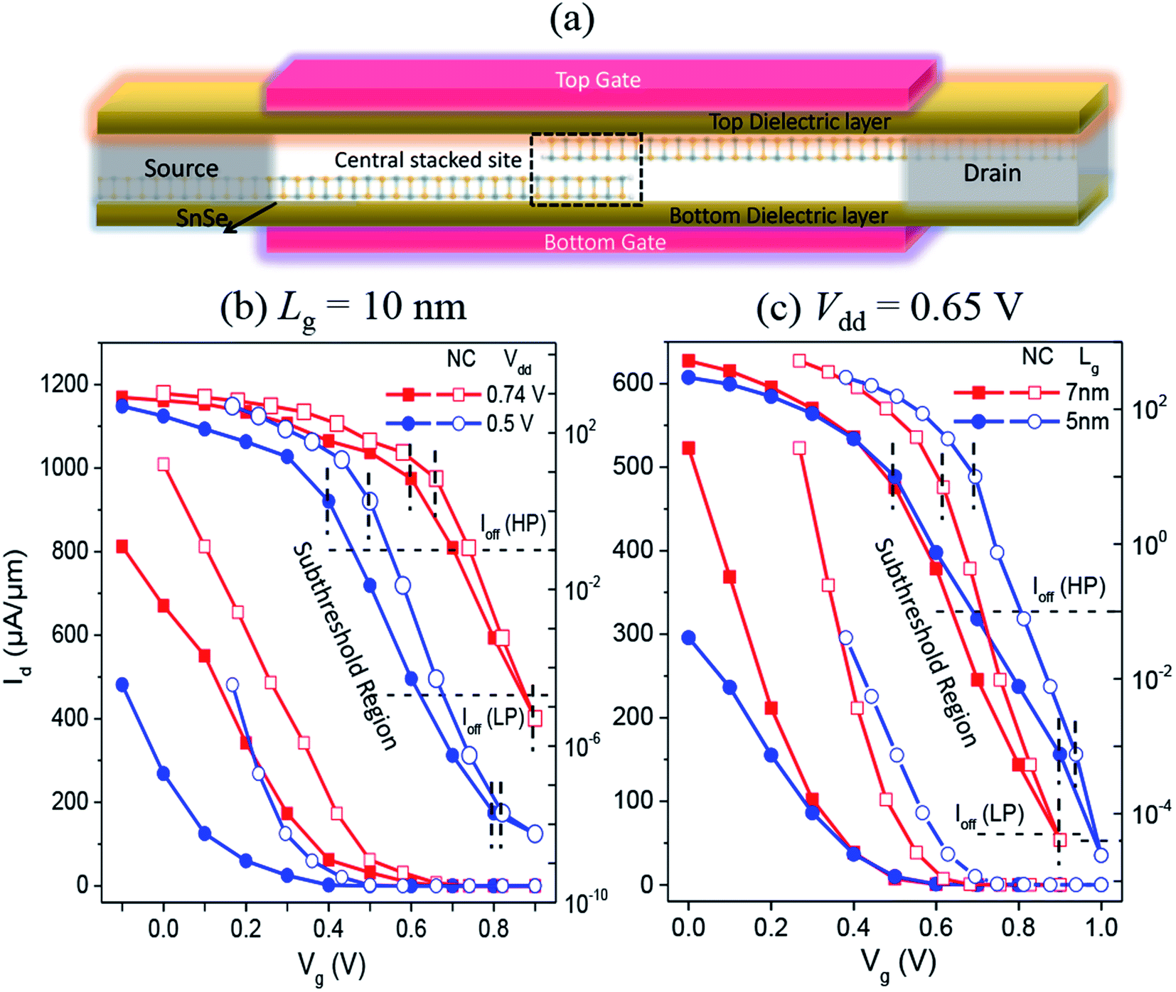 | ||
| Fig. 1 (a) Device model and (b and c) transfer characteristics of the optimal sub-10 nm vertical SnSe homojunction p-TFETs and p-NCTFETs. The subthreshold region is marked with vertical black dash lines. | ||
The vertical SnSe homojunction TFETs are calculated by the DFT coupled with nonequilibrium Green's function (NEGF) using QuantumATK.25,26 We use the same setting parameters as the DFT calculations for device simulations except for 31 × 1 × 151 k-points. It's known that the GGA approximation has underestimate band gaps of intrinsic semiconductors. However, in a device model, the electrodes and channel are in a heavy doped condition, which induces a heavy screening effect to the electron–electron interaction. In the heavy doping case, the GGA approximation becomes a fine approach to the GW method for semiconductor's band gaps as discussed in a previous work.5
The transmission coefficient T(E) is obtained by averaging T(E,kx) over 61 kx-points, where T(E,kx) = Tr[Gr(E,kx)Γs(E,kx)Ga(E,kx)Γd(E,kx)]. Then the current I(Vds,Vg) is then derived from T(E) from the Landauer–Büttiker formula:31
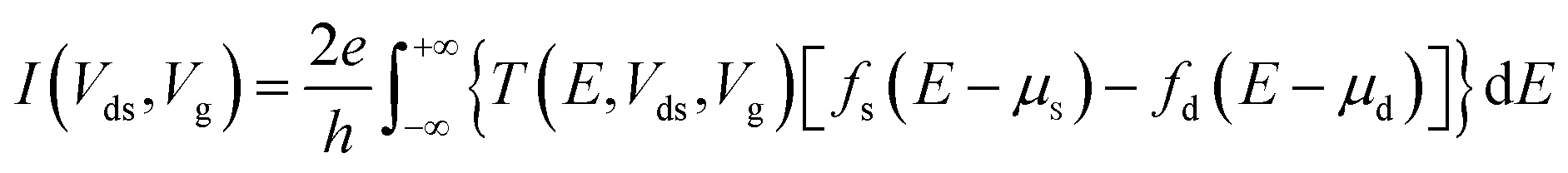
We then use a 100 nm-thick SrBi2Nb2O9 to construct negative capacitance vertical TFETs with the SnSe stacked homojunction, where SrBi2Nb2O9 is the best ferroelectric material among four checked ones for the ML GeSe and GeTe TFETs.32 A negative voltage drop VNC should happen across the ferroelectric layer so that a sharper subthreshold swing is expected. We calculate the VNC with the Landau–Khalatnikov (L–K) theory33 as follows:
| VNC = 2αtFeQ + 4βtFeQ3 + 6γtFeQ5 |
3 Results and discussions
3.1 Device optimization and current
Considering the stacked sites and Ns/Nd might have some effect on currents, we first optimize Ileak and Ion of the 10 nm vertical SnSe homojunction TFET at Vdd = 0.74 V. The transfer characteristics of the vertical SnSe TFETs with stacked sites (fixed Ns/Nd of 5/5 × 1013 cm−2) are given in Fig. S1(a).† Ambipolar characters are seen for the three TFETs as Ns and Nd are the same. All Ileak are ∼10−3 μA μm−1, which are low enough to meet the off-state current (Ioff) of 0.1 μA μm−1 of the HP devices but too high to meet Ioff of 2 × 10⁻⁵ μA μm−1 of the LP devices of the ITRS requirements (2013 version). Thus, we extract Ion from the transfer characteristics for both p- and n-type branches and give the values in Table S2.† The central site of the stacked position is the best one for Ion of both the p- and n-type vertical SnSe TFETs with the values of 791 and 695 μA μm−1, respectively, which meet 61% and 54% of 1287 μA μm−1 of the ITRS HP device.We then pick up the vertical SnSe TFET with the central stacked site and continue to lower Ileak by applying an asymmetric Ns/Nd. In general, the asymmetric Ns/Nd would destroy the ambipolar characters of a TFET, and an improved Ion would be acquired with a light-Ns/heavy-Nd for p-type branch and heavy-Ns/light-Nd for n-type one from previous studies.5–7 The transfer characteristics of the vertical SnSe TFETs with Ns of 1/0.3/0.1 × 1013 cm−2 (fixed Nd of 5 × 1013 cm−2) and Nd of 1/0.3/0.1 × 1013 cm−2 (fixed Ns of 5 × 1013 cm−2) are drawn in Fig. S1(b) and (c),† respectively. A lower Ileak of 10−4–10−7 μA μm−1 and an enhanced p- or n-type character are acquired as expected. Ileak is small enough for LP applications when either Ns or Nd ≤ 0.3 × 1013 cm−2. Benchmark of Ion(HP) and Ion(LP) against the ITRS HP/LP devices and its planar counterpart is presented in Table S3.† For HP application, the asymmetric Ns/Nd does not show a positive effect on Ion. Compared with its planar counterpart at the same Ns/Nd of 1/5 × 1013 cm−2, Ileak decreased from ∼10−2 to ∼10−4 μA μm−1 and Ion(HP) from 1667 to 790 μA μm−1. The descending currents come from the interrupted carrier transport path by the structure modification of vertical stacking. For LP application, the lightest Ns or Nd is the best. In the following, we will focus on the device performances of the enhanced p-type region of the optimal vertical SnSe homojunction TFETs with central stacked sites and Ns/Nd = 0.1/5 × 1013 cm−2 for LP applications.
The transfer characteristics of the sub-10 nm optimal vertical SnSe homojunction p-TFETs are given in Fig. 1(b and c), and the key figures of merit for LP applications are presented in Table 1. As Lg decreases to 7/5 nm, Ileak is also low enough to meet Ioff of 4/5 × 10−5 μA μm−1 of the ITRS LP devices. The ITRS targets for LP devices and the device performances of the planar GeSe,5 planar BP,35 vertical homojunction BP,9 and vertical homojunction antimonene35 TFETs are given for comparison in Table 1. We provide Ion as a function of Ioff of the SnSe homojunction p-TFETs (Lg = 5–10 nm, Vdd = 0.5–0.74 V) and Ion of the devices mentioned above in Fig. 2(a–d). The optimal Ion(LP) are 488, 146, and 62 μA μm−1 for the vertical SnSe p-TFET at Lg = 10, 7, and 5 nm, respectively, which surpass or meet 43% and 21% of 461, 337, and 195 μA μm−1 of the 2022, 2026, and 2028 targets of the ITRS LP devices (2013 version) at similar Lg, respectively. As seen in Fig. 2, when Ioff increases by ∼4 orders of magnitude from ∼10−5 to 10−1 μA μm−1, Ion increases slowly by 1.5–4.1 times, and the increment is more notable for the TFET with a shorter Lg or at a lower Vdd. Though Ion of the vertical SnSe p-TFET show no goodness when compared to other sub-10 nm TFETs, it's worthy to note that Ion of 105 μA μm−1 of the 10 nm vertical SnSe p-TFET is comparable with those of 135–193 μA μm−1 of the vertical antimonene TFET and the planar phosphorene and GeSe TFETs at Vdd = 0.5 V.5,35
| Lg (nm) | Vdd (V) | UL (nm) | Ioff (μA μm−1) | Ion (μA μm−1) | SS (mV dec−1) | gm (mS μm−1) | τ (ps) | PDP (fJ μm−1) | |
|---|---|---|---|---|---|---|---|---|---|
| Vertical SnSe | 10 | 0.74 | 0 | 2 × 10⁻⁵ | 488 | 48.2 | 1.89 | 0.081 | 0.019 |
| Vertical SnSe NCTFET | 10 | 0.74 | 0 | 2 × 10⁻⁵ | 747 | 36.8 | 2.04 | 0.068 | 0.023 |
| Vertical BP9 | 10 | 0.74 | 0 | 2 × 10⁻⁵ | 830 | 39 | 4.30 | 0.029 | 0.027 |
| Planar GeSe5 | 10 | 0.74 | 0 | 2 × 10⁻⁵ | 759 | 45 | 3.92 | 0.062 | 0.035 |
| ITRS 2022 | 10.1 | 0.72 | — | 2 × 10⁻⁵ | 461 | — | — | 1.556 | 0.52 |
| Vertical SnSe | 10 | 0.5 | 0 | 1 × 10⁻⁵ | 105 | 49.0 | 1.78 | 0.346 | 0.011 |
| Vertical SnSe NCTFET | 10 | 0.5 | 0 | 1 × 10⁻⁵ | 404 | 36.7 | 2.77 | 0.133 | 0.017 |
| Vertical Sb35 | 10 | 0.5 | 0 | 1 × 10⁻⁵ | 193 | 22 | — | — | — |
| Planar BP35 | 10 | 0.5 | 0 | 1 × 10⁻⁵ | 135 | 33 | — | — | — |
| Planar GeSe5 | 10 | 0.5 | 0 | 1 × 10⁻⁵ | 146 | — | — | 0.19 | 0.014 |
| Vertical SnSe | 7 | 0.65 | 3 | 4 × 10⁻⁵ | 157 | 74.5 | 1.56 | 0.278 | 0.018 |
| Vertical SnSe NCTFET | 7 | 0.65 | 3 | 4 × 10⁻⁵ | 565 | 47.8 | 1.84 | 0.092 | 0.021 |
| Vertical BP9 | 7 | 0.66 | 0 | 4 × 10⁻⁵ | 350 | 63 | 4.23 | 0.063 | 0.018 |
| ITRS 2026 | 7 | 0.66 | — | 4 × 10⁻⁵ | 337 | — | — | 1.514 | 0.34 |
| Vertical SnSe | 5 | 0.65 | 5 | 5 × 10⁻⁵ | 62 | 91.4 | 0.75 | 0.721 | 0.018 |
| Vertical SnSe NCTFET | 5 | 0.65 | 5 | 5 × 10⁻⁵ | 346 | 60.1 | 1.14 | 0.154 | 0.021 |
| Vertical BP9 | 5 | 0.64 | 5 | 5 × 10⁻⁵ | 312 | 76 | 3.9 | 0.078 | 0.018 |
| ITRS 2028 | 5.9 | 0.64 | — | 5 × 10⁻⁵ | 295 | — | — | 1.493 | 0.28 |
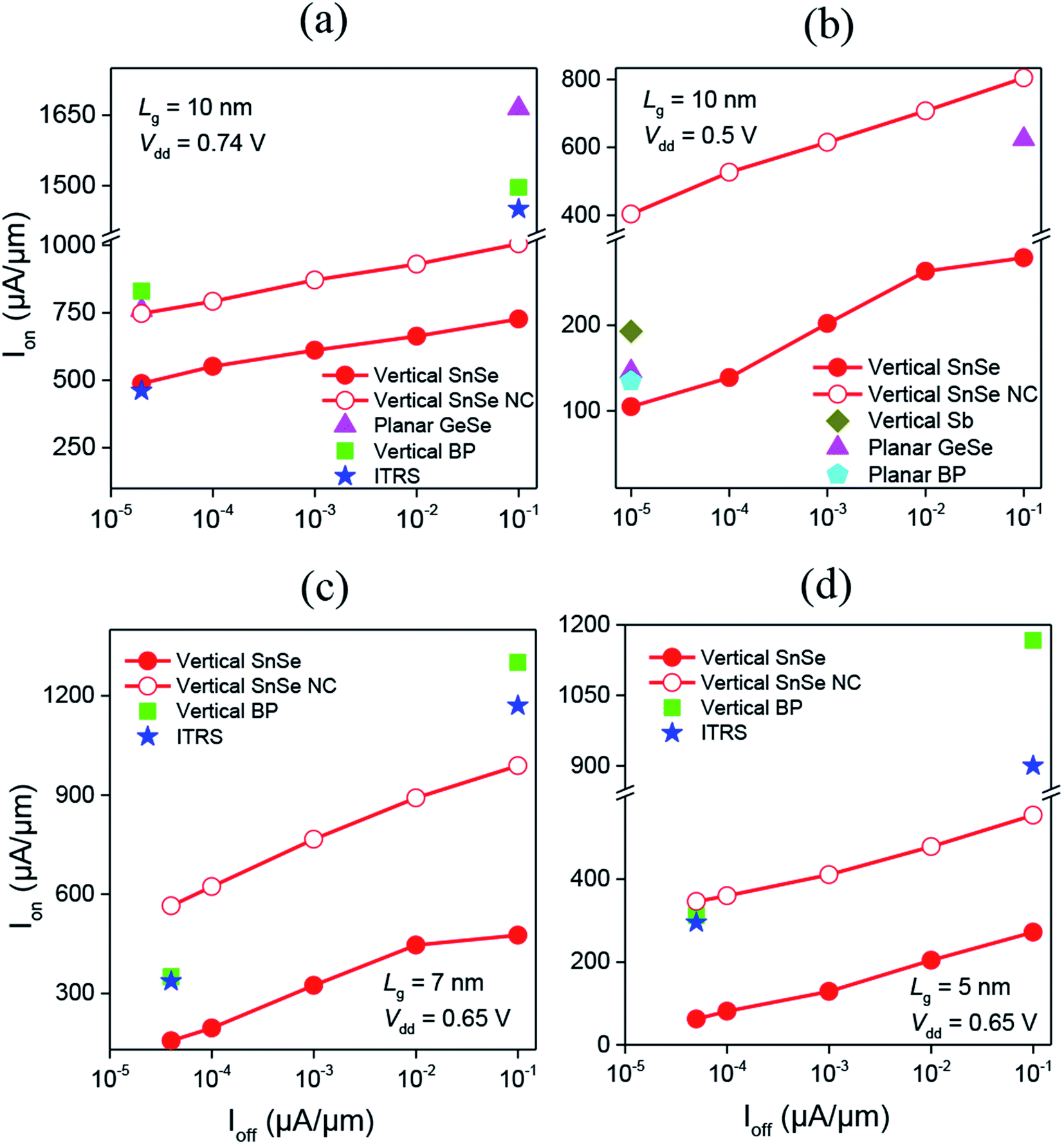 | ||
| Fig. 2 Ion vs. Ioff of the optimal vertical SnSe homojunction p-TFETs and p-NCTFETs with (a) Lg = 10 nm and Vdd = 0.74 V, (b) Lg = 10 nm and Vdd = 0.5 V, (c) Lg = 7 nm and Vdd = 0.65 V, and (d) Lg = 5 nm and Vdd = 0.65 V. Ion of the ITRS requirements for LP and HP devices and those of the planar GeSe,5 planar BP,35 vertical homojunction BP,9 and vertical homojunction antimonene35 TFETs are given for comparison. | ||
3.2 Gate control ability and dynamic performance metrics
The gate control abilities are described by the subthreshold swing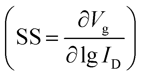 and transconductance
  in the subthreshold and superthreshold regions, respectively. A smaller SS (or a larger gm) stands for a stronger gate control ability. We give SS (in the subthreshold region as marked in Fig. 1) and gm of the sub-10 nm optimal vertical SnSe homojunction p-TFET compared with those of the vertical BP and planar GeSe and SnSe TFETs5,9 in Fig. 3(a and b). The subthreshold regions cover five to eight decades of currents for all the vertical SnSe p-TFETs. Both an increasing SS (48.2 to 91.4 mV dec−1) and decreasing gm (1.89 to 0.75 mS μm−1) with the decreasing Lg are seen for the vertical SnSe p-TFETs, which indicates the descending gate control ability with the decreasing Lg in both subthreshold and superthreshold regions. The slightly larger SS and much smaller gm of the vertical SnSe p-TFETs compared with those of the vertical BP and planar GeSe TFETs5,9 at the same Lg indicate a slightly weaker gate control in the subthreshold region and a much weaker gate control in the superthreshold regions, respectively. Whereas, in regard to its SnSe planar counterpart,5 much enhanced and descended gate controls are found in the subthreshold and superthreshold regions, respectively.
 | ||
| Fig. 3 (a) SS, (b) gm, (c) τ, and (d) PDP as a function of Lg of the optimal sub-10 nm vertical SnSe homojunction p-TFETs and p-NCTFETs (Vdd = 0.64–0.74 V) compared with those of the ITRS requirements for LP devices and those of the planar GeSe5 and vertical homojunction BP.9 | ||
The average SS over four decades of current (SSave_4 dec) and the drain current at SS = 60 mV dec−1 (I60) are regarded as two metrics for fast low-power devices. Basically, SSave_4 dec below 60 mV dec−1 and I60 above 1 μA μm−1 are asked for a fast low-power device. We present the minimum SS (SSmin), SSave_4 dec, and I60 of the vertical SnSe p-TFETs in Table S4.† The sharp SSmin is harder to maintain over decades of current in the vertical SnSe p-TFETs with shorter Lg. Sub-thermionic SSmin and SSave_4 dec and high I60 are only obtained for the 10 nm vertical SnSe p-TFET, i.e., SSmin of 42.0–43.4 mV dec−1, SSave_4 dec of 44.2–45.8 mV dec−1, and I60 of 5–7 μA μm−1 at Vdd = 0.5–0.74 V. For the 7 and 5 nm vertical SnSe p-TFETs, SSmin are 60.7 and 66.7 mV dec−1 and SSave_4 dec are 71.2 and 90.1 mV dec−1, respectively.
The device dynamic performance metrics are represented by the intrinsic delay time 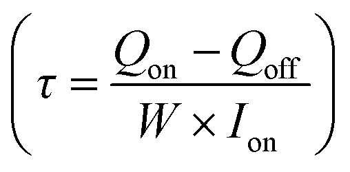 and the power delay product
 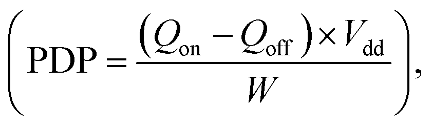 which define the switching speed and energy consumption of a transistor, respectively. Here, Qon/off is the on-/off-state overall charge of the channel and W the channel width. We benchmark τ and PDP of the vertical SnSe p-TFETs against the ITRS LP devices and the planar GeSe and vertical BP TFETs5,9 in Fig. 3(c and d). τ of the vertical SnSe p-TFET increases rapidly from 0.156 to 0.721 ps with the decreasing Lg from 10 to 5 nm, indicating an obvious decaying of the device switching speed with the decreasing Lg. τ of the vertical SnSe p-TFET is half to one-tenth of 1.493–1.556 ps of the ITRS LP devices, but much larger than those of the planar GeSe and vertical BP TFETs at the same Lg. The vertical SnSe p-TFET shows a generally better behavior on energy consumption at a shorter Lg as a decreasing trend of PDP is seen. PDP of 0.018–0.035 fJ μm−1 of the vertical SnSe p-TFET is more than one order of magnitude below the ITRS LP devices (0.28–0.52 fJ μm−1) and nearly equal to those of the planar GeSe and vertical BP TFETs5,9 at the same Lg.
3.3 Negative capacitance
The vertically stacked homojunction has a prominent effect of lowering Ileak of its planar counterpart, but unfortunately, Ion descends as well. We then import negative capacitance to make the SS sharper and therefore to improve Ion. The transfer characteristics of the vertical SnSe p-NCTFETs with a 100 nm-thick ferroelectric layer of SrBi2Nb2O9 are given in Fig. 1(b and c). A remarkable enhanced of Ion by 53–458% is obtained as given in Table 1 and Fig. 2. Ion of 565 and 346 μA μm−1 of the vertical SnSe NCTFETs surpass the 2026 and 2028 targets of 337 and 295 μA μm−1 of the ITRS LP device at Lg = 7 and 5 nm, respectively. At a lower Vdd = 0.5 V, Ion of 404 μA μm−1 of the 10 nm vertical SnSe NCTFET is 2–3 times the vertical antimonene TFET and the planar phosphorene and GeSe TFETs.5,35 The SS and gm of the vertical SnSe NCTFETs are given in Table 1 and Fig. 3(a and b). SS decrease to 36.7–60.1 mV dec−1 and gm increase to 1.14–2.77 mS μm−1, implying an enhanced gate control of the NCTFET counterpart. τ decrease to 0.068–0.154 ps and PDP increase slightly to 0.017–0.023 fJ μm−1 as given in Table 1 and Fig. 3(c and d).3.4 LDDOS, spectral current, and discussion
The local device density of states (LDDOS) together with spectral currents of the vertical SnSe p-TFET at Vg = 1.0 V (leakage current) and 0.0 V (maximum current) compared with its planar counterpart are presented in Fig. 4. An obvious enhanced barrier can be seen from the LDDOS of the vertical SnSe p-TFET for both the leakage-current and maximum-current states, which results in a sound decreasing of spectral currents. As a result, this vertically stacked modification of the SnSe TFET lower the leakage current of its planar counterpart by 2–3 orders of magnetite, but an unwanted descendant of Ion by around a half is accompanied. | ||
| Fig. 4 Local device density of states (LDDOS) and spectral currents of the optimal vertical SnSe homojunction p-TFETs with Lg = 10 nm at Vdd = 0.74 V compared with those of the planar counterpart for the (a) leakage-current state and (b) maximum-current state. | ||
In a word, the structural modification of vertical stacking is a certainly effective solution to lower Ileak of a TFET, and we have succeeded in tuning the SnSe TFET from HP device to LP device in this work and extending the BP TFET to LP application.9 And to import a ferroelectric layer is a remarkable method to improve Ion. Noteworthily, this vertically stacked modification and negative capacitance introduction of a TFET structure is a prototype method, and could easily apply to other 2D planar TFETs, like the Bi and GeTe TFETs,8,32 which possess both high Ileak and Ion simultaneously.
For the realization of 2D FETs in labs, sub-5 nm traditional FETs are reported based on the channel material of ML MoS2,36 bilayer MoS2,37 and bilayer MoTe2.38 For 2D BP traditional FETs, the shortest experiment reported gate length is 20 nm.39 As for 2D TFETs, the progress in experiment is much behind the traditional FETs. To the best of our knowledge, there're no reports of 2D TFETs in the nanometer scale. Recently, the vertical homojunction TFETs based on multilayer BP have been realized in the micrometer scale in labs.40,41 As an analog of BP, 2D SnSe is widely studied in recent years42–44 but rarely reported as FET despite its excellent electronic properties like BP and good air-stability over BP. Our theoretical predicted good device performances of the sub-10 nm vertical SnSe homojunction TFET for a fast LP application would certainly encourage the corresponding experimental studies.
4 Conclusions
To summarize, we investigate the device performances of the sub-10 nm vertical SnSe homojunction TFETs with ab initio quantum transport calculations. The vertically stacked device configuration of the SnSe TFET is beneficial for a fast low-power device in regard to the planar configuration because the broken connected top and bottom layers lead to an enhanced transport barrier. SSave_4 dec of 44.2–45.8 mV dec−1 and I60 of 5–7 μA μm−1 are obtained for the optimal vertical SnSe homojunction TFET with Lg = 10 nm at Vdd = 0.5–0.74 V. In terms of Ion, intrinsic τ, and PDP, the vertical SnSe TFETs and NCTFETs outperform the 2022 and 2028 targets of the ITRS low-power device (2013 version), respectively. The impressive performance of the vertical SnSe TFETs would accelerate future TFET manufacturing.Conflicts of interest
There are no conflicts to declare.Acknowledgements
This work was supported by the National Natural Science Foundation of China (No. 11704008 and 91964101), the Basic Scientific Research Foundation of Beijing Municipal Education Commission (No. 110052971803/031), and the Support Plan of Yuyou Youth and Yuyou Innovation Team, and the fund of high-level characteristic research direction from North China University of Technology.References
- G. Fiori, F. Bonaccorso, G. Iannaccone, T. Palacios, D. Neumaier, A. Seabaugh, S. K. Banerjee and L. Colombo, Nat. Nanotechnol., 2014, 9, 768–779 CrossRef CAS PubMed.
- M. Chhowalla, D. Jena and H. Zhang, Nat. Rev. Mater., 2016, 1, 16052 CrossRef CAS.
- H. Lu and A. Seabaugh, IEEE J. Electron Devices Soc., 2014, 2, 44–49 CAS.
- Y. Lv, W. Qin, C. Wang, L. Liao and X. Liu, Adv. Electron. Mater., 2019, 5, 1800569 CrossRef.
- H. Li, P. Xu and J. Lu, Nanoscale, 2019, 11, 23392–23401 RSC.
- H. Li, B. Shi, Y. Pan, J. Li, L. Xu, X. Zhang, F. Pan and J. Lu, Nanotechnol, 2018, 29, 485202 CrossRef PubMed.
- H. Li, J. Tie, J. Li, M. Ye, H. Zhang, X. Zhang, Y. Pan, Y. Wang, R. Quhe, F. Pan and J. Lu, Nano Res., 2018, 11, 2658–2668 CrossRef CAS.
- H. Li, P. Xu, L. Xu, Z. Zhang and J. Lu, Semicond. Sci. Technol., 2019, 34, 085006 CrossRef CAS.
- H. Li and J. Lu, Appl. Surf. Sci., 2019, 465, 895–901 CrossRef CAS.
- H. Du, X. Lin, Z. Xu and D. Chu, J. Mater. Chem. C, 2015, 3, 8760–8775 RSC.
- A. Carvalho, M. Wang, X. Zhu, A. S. Rodin, H. Su and A. H. Castro Neto, Nat. Rev. Mater., 2016, 1, 16061 CrossRef CAS.
- M. Akhtar, G. Anderson, R. Zhao, A. Alruqi, J. E. Mroczkowska, G. Sumanasekera and J. B. Jasinski, npj 2D Mater. Appl., 2017, 1, 5 CrossRef.
- W. C. Tan, L. Wang, X. Feng, L. Chen, L. Huang, X. Huang and K.-W. Ang, Adv. Electron. Mater., 2019, 5, 1800666 CrossRef.
- J.-S. Kim, Y. Liu, W. Zhu, S. Kim, D. Wu, L. Tao, A. Dodabalapur, K. Lai and D. Akinwande, Sci. Rep., 2015, 5, 8989 CrossRef CAS PubMed.
- D. He, Y. Wang, Y. Huang, Y. Shi, X. Wang and X. Duan, Nano Lett., 2019, 19, 331–337 CrossRef CAS PubMed.
- B. Wan, B. Yang, Y. Wang, J. Zhang, Z. Zeng, Z. Liu and W. Wang, Nanotechnol, 2015, 26, 435702 CrossRef PubMed.
- M.-H. Jeong, D.-H. Kwak, H.-S. Ra, A. Y. Lee and J.-S. Lee, ACS Appl. Mater. Interfaces, 2018, 10, 19069–19075 CrossRef CAS PubMed.
- J. Jiang, C. P. Y. Wong, J. Zou, S. Li, Q. Wang, J. Chen, D. Qi, H. Wang, G. Eda, D. H. C. Chua, Y. Shi, W. Zhang and A. T. S. Wee, 2D Mater., 2017, 4, 021026 CrossRef.
- Y. Huang, L. Li, Y.-H. Lin and C.-W. Nan, J. Phys. Chem. C, 2017, 121, 17530–17537 CrossRef CAS.
- L. Li, Z. Chen, Y. Hu, X. Wang, T. Zhang, W. Chen and Q. Wang, J. Am. Chem. Soc., 2013, 135, 1213–1216 CrossRef CAS PubMed.
- L. Xu, M. Yang, S. J. Wang and Y. P. Feng, Phys. Rev. B, 2017, 95, 235434 CrossRef.
- Y. Guo, S. Zhou, Y. Bai and J. Zhao, ACS Appl. Mater. Interfaces, 2017, 9, 12013–12020 CrossRef CAS PubMed.
- L.-B. Shi, M. Yang, S. Cao, Q. You, Y.-Y. Niu and Y.-Z. Wang, Appl. Surf. Sci., 2019, 492, 435–448 CrossRef CAS.
- L. C. Gomes, A. Carvalho and A. H. C. Neto, Phys. Rev. B, 2016, 94, 054103 CrossRef.
- QuantumATK, version P-2019.03, http://www.synopsys.com/silicon/quantumatk.html Search PubMed.
- S. Smidstrup, T. Markussen, P. Vancraeyveld, J. Wellendorff and K. Stokbro, J. Phys.: Condens. Matter, 2020, 32, 015901 CrossRef CAS PubMed.
- J. P. Perdew, K. Burke and M. Ernzerhof, Phys. Rev. Lett., 1996, 78, 3865–3868 CrossRef PubMed.
- S. Grimme, J. Comput. Chem., 2006, 27, 1787–1799 CrossRef CAS PubMed.
- H. J. Monkhorst, Phys. Rev. B: Solid State, 1976, 13, 5188–5192 CrossRef.
- Y. C. Huang, X. Chen, C. Wang, L. Peng, Q. Qian and S. F. Wang, Nanoscale, 2017, 9, 8616–8622 RSC.
- S. Datta, Electronic Transport in Mesoscopic Systems, Cambridge University Press, Cambridge, England, 1995 Search PubMed.
- P. Xu, J. Liang, H. Li, F. Liu, J. Tie, Z. Jiao, J. Luo and J. Lu, RSC Adv., 2020, 10, 16071 RSC.
- A. Starkov and I. Starkov, Ferroelectrics, 2014, 461, 50–60 CrossRef CAS.
- F. Liu, Y. Zhou, Y. Wang, X. Liu, J. Wang and H. Guo, npj Quantum Mater., 2016, 1, 16004 CrossRef.
- J. Chang, Nanoscale, 2018, 10, 13652–13660 RSC.
- L. Xie, M. Liao, S. Wang, H. Yu, L. Du, J. Tang, J. Zhao, J. Zhang, P. Chen and X. Lu, Adv. Mater., 2017, 29, 1702522 CrossRef PubMed.
- S. B. Desai, S. R. Madhvapathy, A. B. Sachid, J. P. Llinas, Q. Wang, G. H. Ahn, G. Pitner, M. J. Kim, J. Bokor and C. Hu, Science, 2016, 354, 99–102 CrossRef CAS PubMed.
- Q. Zhang, X.-F. Wang, S.-H. Shen, Q. Lu, X. Liu, H. Li, J. Zheng, C.-P. Yu, X. Zhong, L. Gu, T.-L. Ren and L. Jiao, Nat. Electron., 2019, 2, 164–170 CrossRef.
- J. Miao, S. Zhang, L. Cai, M. Scherr and C. Wang, ACS Nano, 2015, 9, 9236–9243 CrossRef CAS PubMed.
- S. Kim, G. Myeong, W. Shin, H. Lim, B. Kim, T. Jin, S. Chang, K. Watanabe, T. Taniguchi and S. Cho, Nat. Nanotechnol., 2020, 15, 203–206 CrossRef CAS PubMed.
- P. Wu and J. Appenzeller, IEEE Electron Device Lett., 2019, 40, 981–984 CAS.
- X. Zhou, Q. Zhang, L. Gan, H. Li, J. Xiong and T. Zhai, Adv. Sci., 2016, 3, 1600177 CrossRef PubMed.
- W. Shi, M. Gao, J. Wei, J. Gao, C. Fan, E. Ashalley, H. Li and Z. Wang, Adv. Sci., 2018, 5, 1700602 CrossRef PubMed.
- W. Huang, C. Li, L. Gao, Y. Zhang, Y. Wang, Z. N. Huang, T. Chen, L. Hu and H. Zhang, J. Mater. Chem. C, 2020, 8, 1172–1197 RSC.
Footnote |
| † Electronic supplementary information (ESI) available: The optimized lattices and band gaps with the PBE, Grimme DFT-D2, and Grimme DFT-D3 functionals; Ion and Ileak of the vertical SnSe TFETs with stacked sites; Ion and Ileak of the vertical SnSe TFETs with Ns/Nd; SSmin, SSave_4 dec, and I60 of the optimal vertical SnSe TFETs; transfer characteristics of the vertical SnSe TFETs with stacked sites and Ns/Nd. See DOI: 10.1039/d0ra03279d |
| This journal is © The Royal Society of Chemistry 2020 |