
 Open Access Article
 This Open Access Article is licensed under a Creative Commons Attribution-Non Commercial 3.0 Unported Licence
Enhanced thermal stability of inverted perovskite solar cells by interface modification and additive strategy†
Xueqing Zheng‡
a,
Tingming Jiang‡b,
Lizhong Baib,
Xu Chenb,
Zeng Chenb,
Xuehui Xub,
Dongdong Songa,
Xiaojian Xua,
Bo Li*a and
Yang (Michael) Yang *b
*b
aDepartment of Applied Physics, College of Science, Zhejiang University of Technology, Hangzhou 310023, People's Republic of China. E-mail: libo@zjut.edu.cn
bState Key Laboratory of Modern Optical Instrumentation, College of Optical Science and Engineering, International Research Center for Advanced Photonics, Zhejiang University, Hangzhou, Zhejiang, People's Republic of China. E-mail: yangyang15@zju.edu.cn
First published on 13th May 2020
Abstract
Inverted perovskite solar cells (PSCs) have recently gained increasing attention because of the long operation lifetime achieved. However, bathocuproine (BCP): a commonly used buffer layer in inverted PSCs, is experimentally confirmed by us to show fast aggregation at the temperature of 85 °C, which is the protocol temperature required by the International Electrotechnical Commission (IEC) standard. This thermal instability of the BCP interfacial layer makes long-term thermal stability of inverted PSCs questionable. Simply removing or replacing it can directly lead to an inferior PCE of a device. We solve this problem by removing the BCP layer and simultaneously increasing the thickness of C60, which obtains a high efficiency of 18% comparable with the device with BCP. This is possibly attributed to the extended migration path of carriers from C60 to metal electrode Ag, consequently reducing the carrier accumulation at the interface. In addition to the interfacial modification, the addition of ionic liquid: BMIMBF4 into perovskite can further improve a device's thermal stability by its effective suppression of perovskite decomposition. The devices with 0.4 mol% of BMIMBF4 exhibit promising thermal stability by retaining 80% of their initial PCE after thermal aging of 400 h at 85 °C.
Introduction
Metal halide perovskite solar cells (PSCs) have achieved rapid progress in the last decade due to the excellent optoelectronic properties of metal halide perovskite semiconductors such as strong light absorption, high charge mobility and long carrier diffusion lengths.1–12 The power conversion efficiency of single-junction PSCs has been boosted from 3.8% (ref. 13) in 2009 to 25.2% (ref. 14) at present based on the regular (n-i-p) structure. As a counterpart of the (n-i-p) structure, PSCs based on inverted (p-i-n) structure have recently gained increasing attention because of their easy fabrication, compatibility with flexible substrates and feasibility of building tandem solar cells.15–19 However, the PCE values of inverted PSCs are generally behind those of devices with regular structure, primarily due to severe non-radiative recombination of charge carriers.17,18,20 Recently, Zheng et al. achieved a record PCE of 22.3% (ref. 21) for inverted PSCs by using long AAL as grain and interface modifiers to favor grain orientation and suppress trap-sate density of the perovskite film, which significantly reduces the PCE gap between the regular and inverted PSCs.Another advantage of inverted PSCs is that they have exhibited longer operational lifetime.22,23 Recently, Bai et al. introduced ionic liquid into perovskite precursor realizing operationally stable inverted PSCs with a PCE drop of only 5% under continuous one sun simulated irradiation for more than 1800 h at 70–75 °C.22 In ref. 21 with the PCE record of 22.3% for inverted PSCs, the devices maintained 100% of the initial efficiency after more than 1000 h at the maximum power point tracking under simulated AM 1.5 illumination, and lost only around 10% of their initial PCE after thermal aging of ∼1020 h under temperature of 85 °C. The above two works represent the most outstanding operational stability and thermal stability of inverted PSCs. However, in the work of Bai et al., the thermal aging test is carried out under 70–75 °C which is lower than the protocol (85 °C) used for commercialized photovoltaic solar module test established by International Electrotechnical Commission (IEC). This is possibly attributed to the intrinsically poor thermal stability of bathocuproine (BCP) ultrathin film which has been commonly used as buffer layer between the electron transport layer and the metal electrode in inverted structure to prevent recombination. Similarly, in the work of X. Zheng et al,21 the authors removed BCP layer instead of a thin layer of SnO2 via atomic layer deposition in order to conduct thermal stability of the device at 85 °C. However, the replacement of BCP layer with SnO2 sacrificed a certain PCE drop from 22.3% to 18%. It seems that whether or not to use BCP layer is a trade-off between thermal stability and efficiency.
In this paper, we focused on the model system of MAPbI3 perovskite, and experimentally demonstrated that the device with BCP interlayer did suffer a fast degradation under thermal stressing at 85 °C, and simply removing BCP layer can cause a severe PCE loss from 18% to 6.97%. In order to solve this dilemma, we have found that getting rid of BCP and meanwhile increasing the thickness of C60 to 80 nm can render the champion device a comparable PCE of 18.1% with the reference device with BCP layer. As a result, the device without BCP layer exhibited almost no PCE loss after thermal aging of 12 h at 85 °C.
Based on this modification, we added 1-butyl-3-tetrafluoroborate (BMIMBF4) ionic liquid into the perovskite precursor to further improve the device thermal stability. Consequently, our device retained 80% of its initial performance following thermal aging at 85 °C for over 400 h.
Experimental details
MAPbI3 perovskite film preparation
The MAPbI3 precursor solution was prepared by dissolving 0.5993 g PbI2 (TCI) and 0.2067 g CH3NH3I (MAI) (TCI) in 900 μL N,N-dimethylmethanamide (DMF) (anhydrous, Sigma-Aldrich) and 100 μL dimethyl-sulfoxide (DMSO) (anhydrous, Sigma-Aldrich). In parallel, we prepared BMIMBF4 ionic liquids (Sigma, 97% purity) containing perovskite precursor solution by dissolving the same components in mixed solvent containing different ionic liquids (proportion and MAPbI3 are between two thousandths and eight thousandths). The MAPbI3 precursors were spin-coated onto ITO/NiOx at 4000 rpm for 50 s. 120 μL sec-pentanol was dropped onto the spinning substrate during the spin-coating. The condition of annealing is under 100 °C for 10 min. Several films grown on bare glass were evaporated with 25 nm C60 for subsequent measurement. The samples for SEM, AFM, XRD measurement were perovskite films spin-coated onto ITO/NiOx. The samples for UV-vis absorption were films grown on bare glass.NiOx film fabrication
7.4 g of nickel nitrate hexahydrate (Sinopharm Chemical Reagent, 98% purity) and 3.31 g of potassium hydroxide (Sinopharm Chemical Reagent, 85% purity) were each dissolved in 50 mL of deionized water. Then, an aqueous potassium hydroxide solution was slowly dropped into an aqueous solution of nickel nitrate. After the two were fully reacted, Ni(OH)2 was centrifuged. After drying Ni(OH)2 at 80 °C for two hours, it was placed in a high temperature furnace at 275 °C for 2 hours to obtain a NiOx nanopowder. Prepare 25 mg mL−1 NiOx solution with powder and spin-coated on cleaned ITO substrates at 3000 rpm. for 30 s and then dried at 25 °C for 30 min.Device fabrication
The pre-patterned ITO substrates were cleaned by ultrasonication in diluted Micro-90 detergent, deionized water, acetone, and isopropanol for 15 min, respectively. NiOx films were coated on the cleaned ITO substrate at 3000 rpm for 30 s and then dried at 25 °C for 30 min. The MAPbI3 perovskite films were deposited by spin-coating the precursor solution onto NiOx film at 4000 rpm for 50 s. sec-Pentanol was dropped onto the spinning substrate during the spin-coating. After spin-coating, some films were annealed immediately under 100 °C for 10 min, while some were firstly stored for 15 min before annealing. Finally, some devices C60 (25 nm)/BCP (5 nm)/Ag (80 nm), while some devices C60 (80 nm)/Ag (80 nm) were sequentially deposited by thermal evaporation to complete the device fabrication.Film and device characterization
Scanning electron microscopy (SEM) images were taken on a Hitachi SU8030 electron microscope. Atomic force microscopy (AFM) images of sample surfaces were obtained on a Cypher S Atomic Force Microscope. The absorption spectrum was measured by Agilient Carry 7000 UV-vis spectrometer. X-ray diffraction measurement was carried out by X-pert Powder. TOPAS-Academic V6 software was used for Rietveld refinements to obtain the lattice parameters. The background and peak shapes were fit using a shifted Chebyshev function with eight parameters and a Pseudo-Voigt function (TCHZ type), respectively. Current density–voltage (J–V) characteristics were measured under AM 1.5G light (1000 W m−2) using the xenon arc lamp of a Class A solar simulator. Light intensity was calibrated using an Newport-calibrated mono crystalline Si diode. The Keithley 2400 source meter was used for I–V measurement. External quantum efficiency (EQE) was characterized with an integrated system (QER3018) from EnliTech. Samples were kept in a N2 filled cell at room temperature for all optical measurements.Results and discussion
The architecture of our standard inverted PSCs is shown in Fig. 1a, which consists of glass/ITO/NiOx/MAPbI3/C60 (25 nm)/BCP (5 nm)/Ag (100 nm). The champion device gives a high PCE of 18.04% with a Voc of 0.98 V, Jsc of 22.21 mA cm−2 and FF of 0.83 under reverse direction, shown in Fig. 1b, and a negligible hysteresis is observed. Fig. S1† shows a histogram of PCE values of 40 devices from different batches, which indicates a high reproducibility of our device fabrication. The J–V curves of device before and after heating at 85 °C are placed in Fig. 1c. It can be observed that the PCE of the device has rapidly dropped to 12.1% from its initial value of 17.1% only for 12 h of thermal aging under 85 °C. In order to understand the factors triggering such rapid device degradation, the XRD measurements for the perovskite films deposited on pristine glass before and after thermal aging have been carried out as shown in Fig. 1d. The XRD pattern of the perovskite film after 12 h of thermal aging at 85 °C remains almost unaltered with that of perovskite film without heating treatment. This result rules out the possibility of perovskite film degradation within 12 h of thermal heating. Therefore, we conjecture that the thin interlayer BCP is likely to be associated with this degradation during the thermal aging process. The AFM images of the BCP film (5 nm) grown on pristine glass before and after thermal aging are shown in Fig. 1e and f. The BCP film after 12 h of heating under 85 °C has exhibited a high level of clustering and aggregation24 which is clearly attributed to thermal heating. Differential Scanning Calorimetry (DSC) thermograph of BCP powder is shown in Fig. S2† which exhibits a slight endotherm peak at about 84.2 °C possibly resulting in the BCP clustering. The appearance of BCP molecule clustering has resulted the root-mean-square roughness of the film increasing from 6.68 nm before thermal aging to 10.42 nm after thermal aging. The increased BCP film roughness can potentially lead to a certain degree of electrical shunting24 of the device that consequently hampers the device performance.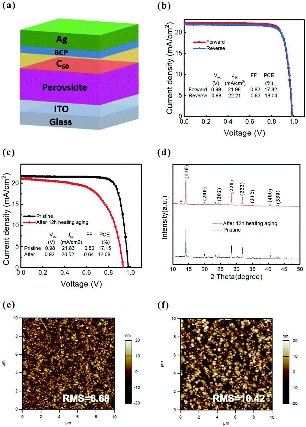 | ||
| Fig. 1 (a) Schematic diagram of our standard p-i-n device structure; (b) J–V curves of the best-performing device under forward and reverse scans with photovoltaic parameters inserted, respectively; (c) histogram of PCEs of 40 devices; (d) J–V curves of devices before and after thermal aging for 12 h under 85 °C AFM images of BCP thin film (5 nm) deposited on glass before; (e) and after (f) thermal aging for 12 h under 85 °C. | ||
The above results have experimentally demonstrated that the BCP molecules undergo aggregation under thermal environment under 85 °C and causes a fast device degradation. Therefore, we tried to simply remove the BCP buffer layer completely as shown in Fig. 2a without any other changes compared with our standard device in Fig. 1a.
 | ||
| Fig. 2 (a) Schematic diagram of the device structure without BCP buffer layer and varied thickness of C60 layer; (b) J–V curves of (C60 thickness: 25 nm for both cases); (c) J–V curves of the standard device with BCP layer (5 nm) and C60 layer (25 nm), and devices without BCP layer and with C60 layer of 80 nm; (d) external quantum efficiency (EQE) spectra and integrated Jsc of the standard device with BCP layer (5 nm) and C60 layer (25 nm), and devices without BCP layer and with C60 layer of 80 nm; (e) histograms of PCEs of standard device with BCP layer (5 nm) and C60 layer (25 nm), and device without BCP layer and with C60 layer of 80 nm over 40 cells; (f) J–V curves of device without BCP layer and with C60 layer of 80 nm before and after thermal aging of 12 h under 85 °C. | ||
However, as shown in Fig. 2b the PCE of the device without BCP layer has evidently dropped to 10% compared with 18.04% of our standard device with BCP buffer layer of 5 nm, which are in accordance with the previous reports:25–27 A Schottky barrier will be formed at the interface when n-type semiconductor C60 is directly contacted with the metal electrode Ag which can give rise to larger interface resistance and charge accumulation at the interface. The introduction of BCP block layer between C60 and Ag can change the Schottky into an ohmic contact and finally contribute to the improvement of device performance. It is noteworthy to point out that the thickness of C60 is just 25 nm in our standard device without BCP layer so that the migration distance of photo-generated electrons from C60 to Ag is shorter which can possibly lead to a large degree of charge accumulation at the interface because the electrons are not able to transport to the Ag in time due to the existence of Schottky barrier. As a result, a severe recombination is likely to occur at the interface resulting in the poor device performance. Therefore, we proposed to increase the thickness of C60 to lengthen the path of electrons from to Ag, which may mitigate the accumulation of carriers at the interface.
The photovoltaic parameters of devices with different thickness of C60 are shown in Table 1. It can be seen that the PCEs of the devices gradually increase as the C60 thickness increases from 25 nm to 80 nm. However, the device efficiency starts to decrease when the thickness of C60 reaches to 100 nm, which is possibly attributed to the too thick layer of C60 resulting in a severe carrier recombination during the transportation of electrons through C60 layer. Based on our results, the increase of C60 thickness in fact contributes to the improvement of the device performance without the BCP blocking layer. The champion device without BCP achieves PCE of 18.12% based on the C60 thickness of 80 nm as shown in Fig. 2c, which is comparable with that of the standard device with BCP layer. And the hysteresis of the device is almost negligible shown in Fig. S3.† It is worth to mention that the Voc of the champion device with C60 thickness of 80 nm and without BCP layer is slightly larger than that of device with BCP (5 nm) and C60 (25 nm) layer as seen in Fig. 2c, which is still likely due to the reduced carrier accumulation at the interface of C60 and Ag benefiting from the longer migration of electron within C60 layer. By contrast, the Jsc of device without BCP is relatively lower than that of device with BCP layer since the existence of BCP buffer layer can anyhow lower down the Schottky barrier and can offer a higher carrier generation yield leading to a higher Jsc.24–26 The Fig. 2d shows the EQE spectra of solar cells with and without BCP layer. Their integrated Jsc values from the EQE spectra are determined to be respectively, which match well with their Jsc obtained from the J–V curves. Fig. 2e exhibits the PCEs histograms of devices with and without BCP layer over 40 samples for each type, which demonstrate a significant overlap. This indicates that our strategy to remove BCP and improve the C60 thickness has reliably achieved the device PCE comparable with the standard device with BCP layer.
| X (nm) | Jsc (mA cm−2) | Voc (V) | FF | PCE (%) |
|---|---|---|---|---|
| 25 | 12.58 | 0.90 | 0.61 | 6.97 |
| 60 | 21.06 | 1.02 | 0.82 | 17.60 |
| 80 | 21.23 | 1.04 | 0.82 | 18.12 |
| 100 | 20.58 | 1.04 | 0.81 | 17.33 |
We proceed to conduct the thermal stability test to the device without BCP layer under 85 °C for 12 h as displayed in Fig. 2f. No PCE loss is observed after thermal aging of 12 h at 85 °C. The removal of BCP layer and increasing the thickness of C60 has not only achieved comparable device PCE with the standard device with BCP layer, but also solved the instability issue of BCP molecules under 85 °C heating which lays the foundation of further improving the thermal stability of our inverted PSCs.
Introducing additives to perovskite is one of the most effective methods to improve PSCs stability.28,29 To further improve the thermal stability of the inverted PSCs, an ionic liquid 1-butyl-3-methylimidazolium tetrafluoroborate with the chemical structure shown in Fig. 3a (BMIMBF4 in short) is incorporated into the perovskite film based on the study22 of S. Bai et al. The J–V curves of the devices with BMIMBF4 concentration varying from 0 to 0.8 mol% are exhibited in Fig. 3b, the corresponding statistics of PCE is shown in Fig. 3c. The PCEs of the devices with BMIMBF4 concentration of 0.2 mol% and 0.4 mol% remain almost unchanged with respect to the control device without BMIMBF4 addition. And there is no evident hysteresis caused by the introduction of BMIMBF4 shown in Fig. S4,† in contrast to the work of Bai et al., in which significant hysteresis occurred after the addition of BMIMBF4. In addition, the morphology and crystallization of perovskite films with and without BMIMBF4 also show no obvious changes from the observations of SEM images and XRD patterns in Fig. S5.† However, to further increase the concentration of BMIMBF4 over 0.4 mol% results in decreased PCEs of the devices mainly reflected in the FF loss. After 400 h of thermal aging at 85 °C shown in Fig. 3d, the control device without BMIMBF4 exhibits a fast degradation and only retains less than 30% of its initial PCE, while the devices with BMIMBF4 of 0.2 and 0.4 mol% retain 60% and 80% of their initial values, respectively. It indicates that the optimal concentration of BMIMBF4 is about 0.4 mol% which endows the corresponding device with the best performance against thermal aging at 85 °C (Table 2).
 | ||
| Fig. 3 (a) Chemical structure of the ionic liquid BMIMBF4; (b) current density–voltage (J–V) curves of device with the configuration of ITO/NiOx (20 nm)/perovskite (500 nm)/C60 (80 nm)/Ag (100 nm) containing different concentration of BMIMBF4 from 0.2 to 0.8 mol% with respect to the stoichiometric amount of perovskite MAPbI3; (c) statistics of device PCE using perovskite precursors with a BMIMBF4 concentration ranging from 0.2% to 0.8%; (d) thermal stability of devices with a varying concentration of BMIMBF4 at a fixed temperature of 85 °C in a N2 atmosphere. | ||
| Ratio | Jsc (mA cm−2) | Voc (V) | FF | PCE (%) |
|---|---|---|---|---|
| 0 | 21.32 | 1.04 | 0.82 | 18.13 |
| 0.2 mol% | 21.01 | 1.03 | 0.83 | 17.96 |
| 0.4 mol% | 21.46 | 1.04 | 0.81 | 18.07 |
| 0.6 mol% | 21.15 | 1.04 | 0.74 | 16.31 |
| 0.8 mol% | 21.18 | 1.05 | 0.68 | 15.20 |
To elucidate the mechanism of BMIMBF4 for enhancing the thermal stability of the devices, we carried out thermal stability test to the perovskite films without (as control) and with BMIMBF4 addition for 100 h under 85 °C heating, and the XRD patterns of the corresponding perovskite films are recorded shown in Fig. 4a and b. From the XRD pattern of the control film, a strong peak at 14.2° appeared which is indexed as the peak of PbI2. The appearance of PbI2 typically originates from the decomposition of perovskite MAPbI3 caused by the long-term heating pressure according to previous studies.30–34 The MAPbI3 perovskites can decompose to form PbI2 at elevated temperatures even without exposure to oxygen and water consequently resulting in the PCE decline of the MAPbI3 based PSCs. However, the PbI2 peak of the perovskite film with BMIMBF4 addition is quite small which demonstrates that the BMIMBF4 can effectively suppress the decomposition of MAPbI3 perovskites at high temperatures accountable for the improved thermal stability of the devices with BMIMBF4 addition.
 | ||
| Fig. 4 (a and b) XRD patterns of pristine and aged samples of control film and film containing BMIMBF4 (0.4%) on NiOx/ITO coated glass substrates after 100 h under 85 °C; (c and d) the modeled and experimental J–V characteristics of PSCs without and with BMIMBF4 after 400 h heating aging with 85 °C (in a glove box filled with nitrogen). | ||
We employed a modified detailed balance mode10,15,35 to understand the PCE loss mechanism of the devices caused by the decomposition of MAPbI3 perovskites under long-term thermal aging from the point view of device physics. This model is governed by the formula below:

| Thermal aging of 400 h | γ (107 m3 s−1) | Rs (10−4 ohm m2) | Rsh (ohm m2) |
|---|---|---|---|
| With BMIMBF4 | 4.8 | 7.46 | 2.7 × 10⁴ |
| W/O BMIMBF4 | 1.7 × 10³ | 6.75 | 1.4 × 10⁻⁴ |
Conclusions
In summary, we have experimentally demonstrated that the BCP buffer commonly used in inverted PSCs undergoes molecule clustering and aggregation rapidly under thermal aging at 85 °C leading to a fast degradation of device performance which are impossible to fulfill the requirement of long-term thermal stability. But simply removing the BCP layer results in an inferior PCE of the solar cells. We have found that the PCEs of the devices without BCP buffer layer gradually improves as the thickness increase of electron transport layer (C60 used in our case), which is possibly due to extended migration path of carriers from C60 to metal electrode Ag consequently reducing the carrier accumulation at the interface. The PCE of champion device without BCP layer is comparable with the standard device with BCP layer. An optimal amount of BMIMBF4 is added into perovskite precursor to further improve the device thermal stability due to its effective inhibition of MAPbI3 perovskite decomposition evidenced from the suppressed PbI2 XRD peak as a typical decomposition byproduct. Finally, the device with 0.4 mol% BMIMBF4 retains 80% of its initial efficiency after 400 h of thermal aging at 85 °C, which is one of the best results for inverted PSCs in terms of thermal stability. This work represents promising guidelines for commercialization of PSCs in thermal stability test at protocol temperature 85 °C in light of device structure modification and perovskite additive strategy.Conflicts of interest
There are no conflicts to declare.Acknowledgements
The authors want to acknowledge the financial support received from National Key Research and Development Program of Zhejiang Province (2018C04SA170313); Outstanding Youth fund of Zhejiang Natural Science Foundation of China (LR18F050001); Natural Science Foundation of China (61804134); Zhejiang Provincial Natural Science Foundation of China under Grant No. LY14F040003.References
- Q. Dong, Y. Fang, Y. Shao, P. Mulligan, J. Qiu, L. Cao and J. Huang, Solar cells. Electron-hole diffusion lengths > 175 mum in solution-grown CH3NH3PbI3 single crystals, Science, 2015, 347, 967–970 CrossRef CAS PubMed.
- M. Liu, M. B. Johnston and H. J. J. N. Snaith, Efficient planar heterojunction perovskite solar cells by vapour deposition, Nature, 2013, 501, 395–398 CrossRef CAS PubMed.
- J. Burschka, N. Pellet, S.-J. Moon, R. Humphry-Baker, P. Gao, M. K. Nazeeruddin and M. Grätzel, Sequential deposition as a route to highperformance perovskite-sensitized solar cells, Nature, 2013, 499, 316–319 CrossRef CAS PubMed.
- M. Abdi-Jalebi, Z. Andaji-Garmaroudi, S. Cacovich, C. Stavrakas, B. Philippe, J. M. Richter, M. Alsari, E. P. Booker, E. M. Hutter and A. J. Pearson, Maximizing and stabilizing luminescence from halide perovskites with potassium passivation, Nature, 2018, 555, 497–501 CrossRef CAS PubMed.
- T. Jiang, Z. Chen, X. Chen, X. Chen, X. Xu, T. Liu, L. Bai, D. Yang, D. Di, W. E. Sha, H. Zhu and Y. Yang, Power Conversion Efficiency Enhancement of Low-Bandgap Mixed Pb–Sn Perovskite Solar Cells by Improved Interfacial Charge Transfer, ACS Energy Lett., 2019, 4, 1784 CrossRef CAS.
- D. Bi, C. Yi, J. Luo, J.-D. Décoppet, F. Zhang, S. M. Zakeeruddin, X. Li, A. Hagfeldt and M. Grätzel, Polymer-templated nucleation and crystal growth of perovskite films for solar cells with efficiency greater than 21%, Nat. Energy, 2016, 1, 1 Search PubMed.
- H. Tsai, W. Nie, J.-C. Blancon, C. C. Stoumpos, R. Asadpour, B. Harutyunyan, A. J. Neukirch, R. Verduzco, J. J. Crochet and S. Tretiak, High-efficiency two-dimensional Ruddlesden-Popper perovskite solar cells, Nature, 2016, 536, 312–316 CrossRef CAS PubMed.
- X. Li, D. Bi, C. Yi, J.-D. Décoppet, J. Luo, S. M. Zakeeruddin, A. Hagfeldt and M. Grätzel, A vacuum flash-assisted solution process for highefficiency large-area perovskite solar cells, Science, 2016, 353, 58–62 CrossRef CAS PubMed.
- Q. Jiang, Y. Zhao, X. Zhang, X. Yang, Y. Chen, Z. Chu, Q. Ye, X. Li, Z. Yin and J. You, Surface passivation of perovskite film for efficient solar cells, Nat. Photonics, 2019, 13, 460–466 CrossRef CAS.
- T. Jiang, Z. Chen, X. Chen, T. Liu, X. Chen, W. E. Sha, H. Zhu and Y. Yang, Realizing High Efficiency over 20% of Low-Bandgap Pb–Sn-Alloyed Perovskite Solar Cells by In Situ Reduction of Sn4+, Sol. RRL, 2019, 1900467 Search PubMed.
- D. Zhao, C. Chen, C. Wang, M. M. Junda, Z. Song, C. R. Grice, Y. Yu, C. Li, B. Subedi and N. J. Podraza, Efcient two-terminal all-perovskite tandem solar cells enabled by high-quality low-bandgap absorber layers, Nat. Energy, 2018, 3, 1093–1100 CrossRef CAS.
- R. Zhuang, X. Wang, W. Ma, X. Wu, X. Chen, L. Tang, H. Zhu, J. Liu, L. Wu, W. Zhou, X. Liu and Y. Yang, Highly sensitive X-ray detector made of layered perovskite-like (NH4)3Bi2I9 single crystal with anisotropic response, Nat. Photonics, 2019, 13, 602–608 CrossRef CAS.
- A. Kojima, K. Teshima, Y. Shirai and T. Miyasaka, Organometal halide perovskites as visible-light sensitizers for photovoltaic cells, J. Am. Chem. Soc., 2009, 131, 6050–6051 CrossRef CAS PubMed.
- National Renewable Energy Laboratory, Best research-cell efciencies, 2019, www.nrel.gov/pv/assets/pdfs/pv-efciency-chart.20190103.pdf Search PubMed.
- K. A. Bush, A. F. Palmstrom, J. Y. Zhengshan, M. Boccard, R. Cheacharoen, J. P. Mailoa, D. P. McMeekin, R. L. Hoye, C. D. Bailie and T. Leijtens, 23.6%-efficient monolithic perovskite/silicon tandem solar cells with improved stability, Nat. Energy, 2017, 2, 17009 CrossRef CAS.
- W. Chen, Y. Wu, Y. Yue, J. Liu, W. Zhang, X. Yang, H. Chen, E. Bi, I. Ashraful and M. Grätzel, Efficient and stable large-area perovskite solar cells with inorganic charge extraction layers, Science, 2015, 350, 944 CrossRef CAS PubMed.
- D. Luo, W. Yang, Z. Wang, A. Sadhanala, Q. Hu, R. Su, R. Shivanna, G. F. Trindade, J. F. Watts and Z. Xu, Enhanced photovoltage for inverted planar heterojunction perovskite solar cells, Science, 2018, 360, 1442–1446 CrossRef CAS PubMed.
- X. Zheng, B. Chen, J. Dai, Y. Fang, Y. Bai, Y. Lin, H. Wei, X. C. Zeng and J. Huang, Defect passivation in hybrid perovskite solar cells using quaternary ammonium halide anions and cations, Nat. Energy, 2017, 2, 17102 CrossRef CAS.
- J. Zhao, X. Zheng, Y. Deng, T. Li, Y. Shao, A. Gruverman, J. Shield and J. Huang, Is Cu a stable electrode material in hybrid perovskite solar cells for a 30-year lifetime?, Energy Environ. Sci., 2016, 9, 3650–3656 RSC.
- S.-H. Turren-Cruz, A. Hagfeldt, M. Saliba, S.-H. Turren-Cruz, A. Hagfeldt and M. Saliba, Methylammonium-free, high-performance, and stable perovskite solar cells on a planar architecture, Science, 2018, 362, 449–453 CrossRef CAS PubMed.
- X. Zheng, Y. Hou, C. Bao, J. Yin, F. Yuan, Z. Huang, K. Song, J. Liu, J. Troughton and N. Gasparini, Managing grains and interfaces via ligand anchoring enables 22.3%-efficiency inverted perovskite solar cells, Nat. Energy, 2020, 5, 131 CrossRef CAS.
- S. Bai, P. Da, C. Li, Z. Wang, Z. Yuan, F. Fu, M. Kawecki, X. Liu, N. Sakai and J. T.-W. Wang, Planar perovskite solar cells with long-term stability using ionic liquid additives, Nature, 2019, 571, 245–250 CrossRef CAS PubMed.
- S. Yang, S. Chen, E. Mosconi, Y. Fang, X. Xiao, C. Wang, Y. Zhou, Z. Yu, J. Zhao and Y. Gao, Stabilizing halide perovskite surfaces for solar cell operation with wide-bandgap lead oxysalts, Science, 2019, 365, 473–478 CrossRef CAS PubMed.
- F. Jafari, B. R. Patil, F. Mohtaram, A. L. F. Cauduro, H.-G. Rubahn, A. Behjat and M. Madsen, Inverted organic solar cells with non-clustering bathocuproine (BCP) cathode interlayers obtained by fullerene doping, Sci. Rep., 2019, 9, 1 CrossRef CAS PubMed.
- C. Chen, S. Zhang, S. Wu, W. Zhang, H. Zhu, Z. Xiong, Y. Zhang and W. Chen, Effect of BCP buffer layer on eliminating charge accumulation for high performance of inverted perovskite solar cells, RSC Adv., 2017, 7, 35819 RSC.
- N. Shibayama, H. Kanda, T. W. Kim, H. Segawa and S. Ito, Design of BCP buffer layer for inverted perovskite solar cells using ideal factor, APL Mater., 2019, 7, 031117 CrossRef.
- C. He, F. Zhang, X. Zhao, C. Lin and M. Ye, Interface Engineering of BCP Buffer Layers in Planar HeterojunctionPerovskite Solar Cells With NiOx Hole Transporting Layers, Front. Phys., 2018, 6, 99 CrossRef.
- L. Wang, H. Zhou and J. Hu, A Eu3+-Eu2+ ion redox shuttle imparts operational durability to Pb-I perovskite solar cells, Science, 2019, 366, 749–753 CrossRef PubMed.
- M. Kim, G. Kim and T. K. Lee, Methylammonium chloride induces intermediate phase stabilization for efficient perovskites solar cells, Joule, 2019, 3, 2179–2192 CrossRef CAS.
- N.-K. Kim, Y. H. Min, S. Noh, E. Cho, G. Jeong, M. Joo, S.-W. Ahn, J. S. Lee, S. Kim and K. Ihm, Investigation of Thermally Induced Degradation in CH3NH3PbI3 Perovskite Solar Cells using In situ Synchrotron Radiation Analysis, Sci. Rep., 2017, 7, 4645 CrossRef PubMed.
- B. Conings, J. Drijkoningen, N. Gauquelin, A. Babayigit, J. D'Haen, L. D'Olieslaeger, A. Ethirajan, J. Verbeeck, J. Manca and E. Mosconi, Intrinsic Thermal Instability of Methylammonium Lead Trihalide Perovskite, Adv. Energy Mater., 2015, 5, 1500477 CrossRef.
- G. Divitini, S. Cacovich, F. Matteocci, L. Cinà, A. Di Carlo and C. Ducati, In situ observation of heat-induced degradation of perovskite solar cells, Nat. Energy, 2016, 1, 15012 CrossRef CAS.
- B. Philippe, B.-W. Park, R. Lindblad, J. Oscarsson, S. Ahmadi and E. M. J. Johansson, Chemical and electronic structure characterization of lead halide perovskites and stability behavior under different exposures—a photoelectron spectroscopy investigation, Chem. Mater., 2015, 27, 1720–1731 CrossRef CAS.
- E. J. Juarez-Perez, L. K. Ono, M. Maeda, Y. Jiang, Z. Hawash and Y. Qi, Photodecomposition and thermal decomposition in methylammonium halide lead perovskites and inferred design principles to increase photovoltaic device stability, J. Mater. Chem. A, 2018, 6, 9604 RSC.
- W. E. Sha, H. Zhang, Z. S. Wang, H. L. Zhu, X. Ren, F. Lin, A. K. Y. Jen and W. C. Choy, Quantifying Efficiency Loss of Perovskite Solar Cells by a Modified Detailed Balance Model, Adv. Energy Mater., 2018, 8, 1701586 CrossRef.
Footnotes |
| † Electronic supplementary information (ESI) available. See DOI: 10.1039/d0ra03238g |
| ‡ These authors contributed equally. |
| This journal is © The Royal Society of Chemistry 2020 |