DOI:
10.1039/D0RA03043K
(Paper)
RSC Adv., 2020,
10, 23842-23853
Study of a nanocrystalline cobalt coating prepared by area-selective electrodeposition
Received
4th April 2020
, Accepted 16th June 2020
First published on 23rd June 2020
Abstract
Nanocrystalline Co coatings were successfully prepared on the surface of a steel substrate by droplet contact electrodeposition. Area-selective electrodeposition is performed by electrolyte drops contacting the surface of the substrate. By analyzing the current–time curve during the preparation of the coating, the influence of the selected area deposition pattern on the current–time curve is summarized. Meanwhile, microscopic observation, phase composition analysis, and performance testing of the coating were performed. The results show that the control procedure and deposition method directly affect the organization, morphology, and quality of the coating. The limited electrodeposition area and its continuous movement increase the nucleation rate and limit the growth of crystal nuclei. Therefore, the area-selective electrodeposition method has great advantages in preparing nanocrystals. The nanocrystalline Co coating was prepared on the surface of a steel substrate, and the surface hardness and corrosion resistance were improved.
1 Introduction
Prolonging the service life of parts by preparing surface coatings is a common method in engineering applications, and nanocrystalline metal coatings usually have better performance and life due to the small grains.1–3 Among them, electrodeposition technology has been the focus of research on the preparation of nanocrystalline metal coatings due to its mature technology, low cost, and no heat loss to the substrate.4 The nanocrystalline metal coating is attributed with fine grains, which have a good binding force with the substrate, and has excellent mechanical and protective properties.5 Electrodeposition of nanocrystalline Co coatings has attracted more and more attention due to their excellent properties and important role in the military and industry.6–9 Meanwhile, Cr produces toxic substances during the preparation process, and cobalt (Co) is considered to be one of the suitable materials that can replace Cr for protection and decoration.10–14
Area-selective electrodeposition is the electrochemical deposition of metal deposits on localized areas, which can enhance and modify localized areas on the substrate surface. Compared with traditional electrodeposition, area-selective electrodeposition is easier to achieve higher current density in the deposition area, and therefore it is easier to form nanocrystalline. Thus, nanocrystalline Co coating prepared by area-selective electrodeposition has better advantages and flexibility. At present, area-selective electrodeposition technologies mainly include jet electrodeposition (Jet-ECD)15 and brush plating.16 Brush plating and Jet-ECD are mature and widely used in the industrial field due to the characteristics of simple equipment structure, portable operation, and area-selective electrodeposition on a macro scale. Among them, brush plating and Jet-ECD have advantages in the surface electrodeposition of special-shaped structures such as bearings, which makes it still applied to the rapid deposition and repair of metal materials.16–19 In actual operation, the spray plating of the brush plating and the electrospray plating solution will cause pollution to the working environment, and manual operation is required to perform electrodeposition in different pattern areas. Meanwhile, the two-electrode system is still used in the existing research on electrospray deposition and brush plating, which lacks sufficient analysis of current–time data. At the same time, research on area-selective electrodeposition Co coatings is still blank.
Therefore, based on the existing research,20,21 this article reconstructs the original area-selective electrodeposition equipment and uses a three-electrode system to obtain the current–time data during the area-selective electrodeposition process. The morphology, phase, and performance of the Co electrodeposited Co coatings were studied through the change of potential, which provided a research basis for expanding the study of area-selective electrodeposition.
2 Experimental
2.1 The principle
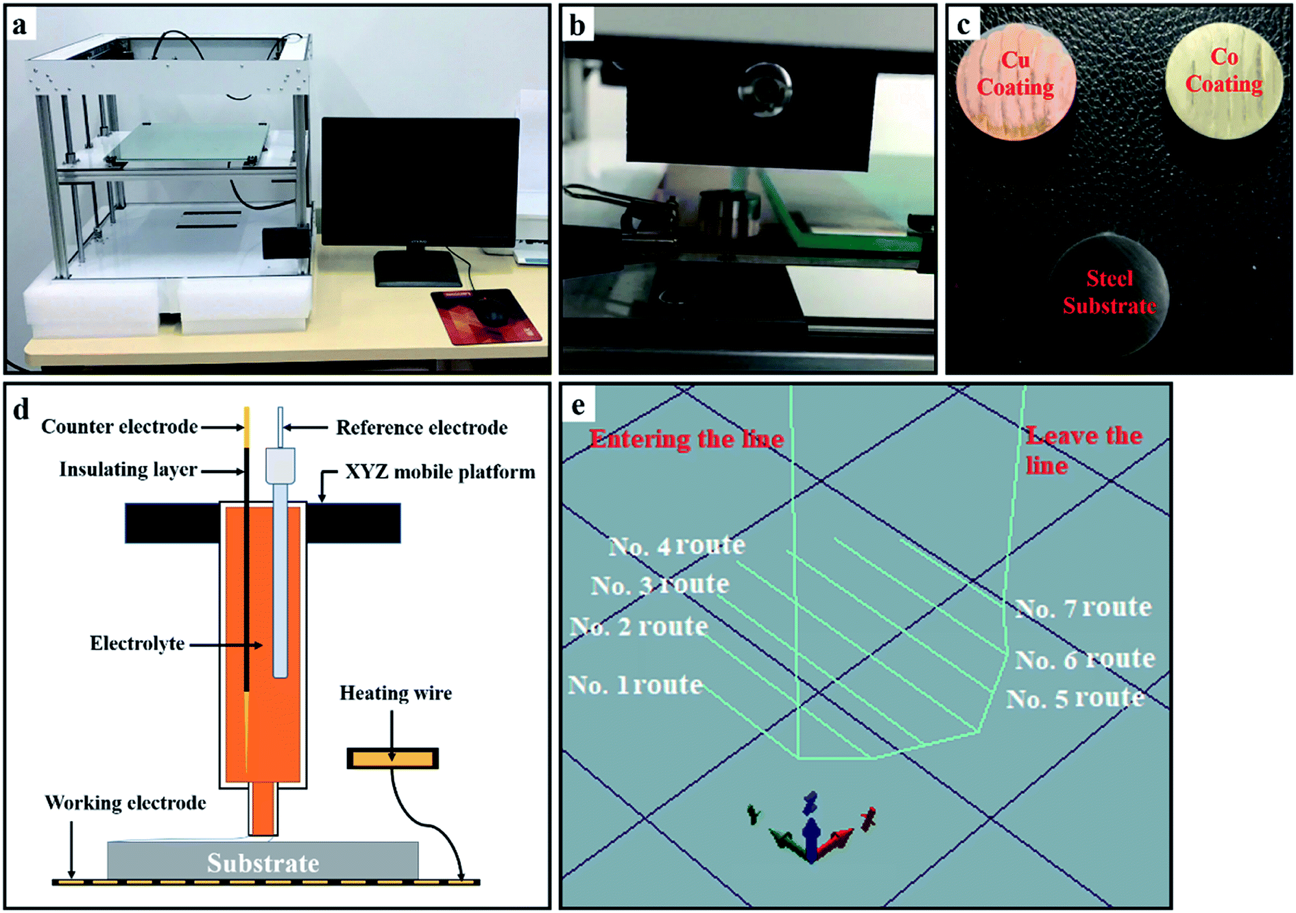
The schematic diagram of area-selective electrodeposition is as shown in Fig. 1, which realizes the preparation of a coating by the droplets contacting (Droplets Contacting Electrodeposition, DCE) the surface of the substrate. The DCE device mainly realizes the coating preparation by controlling the potential, electrodeposition time, temperature, route program, and electrolyte composition. The potential is provided by an electrochemical workstation, and the electrodeposition temperature is used to heat the substrate through an electric heating wire below the substrate. The temperature ranges from room temperature (18 °C) to 100 °C. The deposition path program is implemented by the open-source program code. The DCE device structure is shown in Fig. 1d. Before the deposition starts, the platform needs to be heated, and heat is further transferred to the surface of the substrate in the following manner. The deposition pattern of the substrate surface consisted of seven routes depositions with a width of 2.5 ± 0.2 mm (Fig. 1e) and 4 repetitions per route (18 mm min−1).
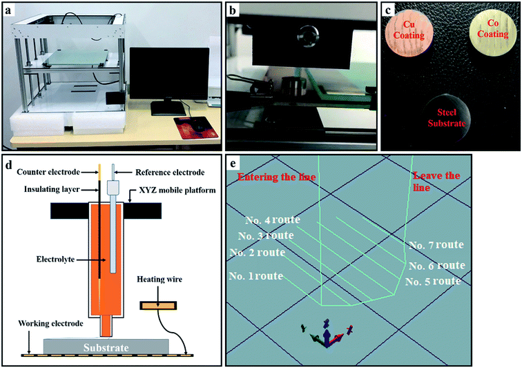 |
| | Fig. 1 (a) The DCE device photo. (b) Photo of the area-selective deposition process. (c) Sample photos. (d) The DCE device schematic. (e) 3D image of the area-selective electrodeposition route. | |
In this experiment, steel was used as the substrate (ASTM: 1045, Table 1), and the size was a cylinder with a diameter of 14 mm and a height of 4 mm. Polish the surface of the substrate with W7, W10, and W20 sandpaper until there are no scratches on the surface. Sonicate the sample with alcohol (analytical grade) for 10 minutes, blow with N2 dry, and store it in a sealed container. Place the substrate on the platform and preheat the substrate by heating the platform to 25 °C for 10 minutes. The electrolyte consisted of 250 g L−1 of CoSO4·7(H2O), Saccharin 5 g L−1 and 1 g L−1 of C18H29NaO3S (pH = 4.5) (Table 2).
Table 1 Elemental composition of steel (ASTM: 1045)
| Element (wt%) |
Content |
| Fe |
>96.51 |
| C |
0.41–0.51 |
| Si |
0.18–0.38 |
| Mn |
0.51–0.81 |
| P |
≤0.036 |
| S |
≤0.034 |
| Cr |
≤0.24 |
| Ni |
≤0.24 |
| Cu |
≤0.23 |
Table 2 Electrodeposition process parameters
| Samples |
a |
b |
c |
d |
| Current (V) |
−2 |
−2.5 |
−3 |
−3.5 |
2.2 Characterization techniques
The electrochemical workstation equipment is CHI660E produced by Shanghai ChengHua Co., Ltd. The crystalline phase of the Co coatings was analyzed by X-ray diffraction (XRD), and the incident angle was 1°. The surface of the coating was observed and analyzed by field emission scanning electron microscope (FESEM) and X-ray photoelectron spectroscopy (XPS). Surface topography data were obtained by atomic force microscopy (AFM). The microhardness test is performed in the area of 5 × 5 mm in the center of the coating surface, and one point is tested every 1 mm. After immersing the sample in a 3.5 wt% NaCl solution for one hour, the Tafel corrosion performance test was performed (Table 3). The corrosion test equipment was inspected by the CHI600E electrochemical workstation. The reference electrode was saturated calomel and the counter electrode was platinum (1 × 1 cm).
Table 3 Working parameters of the corrosion tests
| Working parameters |
| Init E (V) |
0 |
| Final E (V) |
−1 |
| Sweep segment |
1 |
| Hold time at final E (s) |
0 |
| Scan rate (V s−1) |
0.01 |
| Quiet time (s) |
1 |
| Sensitivity (A V−1) |
1 × 10⁻² |
3 Results and discussion
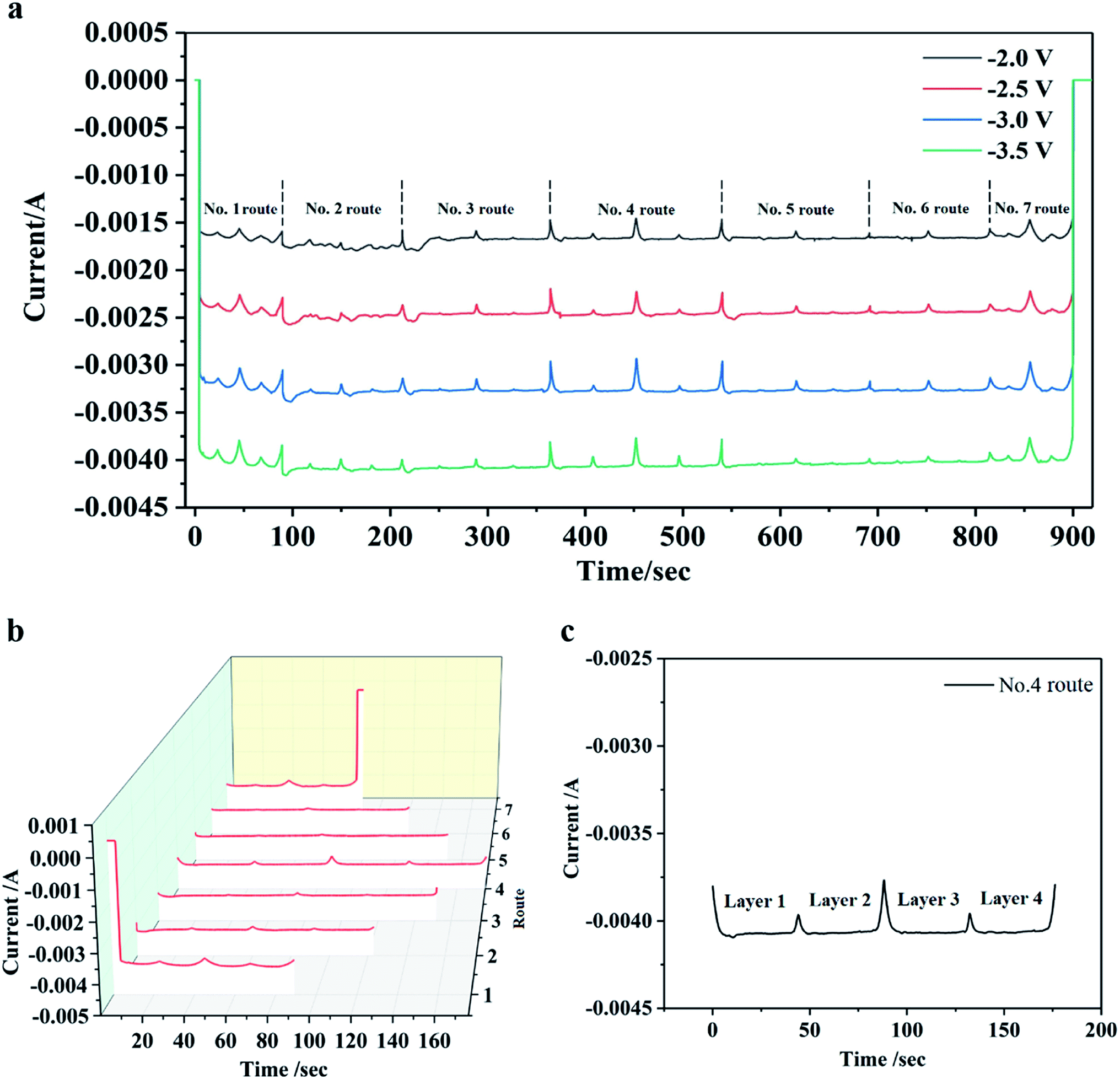
The Fig. 2 shows the constant potential curve of Co at different deposition potentials and its −3 V potential I–T curve decomposition diagram. It can be reflected that as the potential increases, the deposition current regularity increases, and the 7 sedimentary routes are also fed back in the I–T curve. Combined with Fig. 1b, different sedimentary route lengths correspond to different deposition times. Fig. 2b shows that the deposition time of each route is directly related to the graphical design of the program. The No. 4 route is the longest in length and the maximum sedimentary time width in Fig. 2. The I–T curves corresponding to the No. 1 and No. 7 routes have larger fluctuations than No. 4. The reason for this phenomenon is that both No. 1 and No. 7 routes are at the edge of the circular substrate, and the electrodeposited area changes as the electrolyte droplet move. Thus, in addition to the edge routes, other routes have more stable current signals. In the I–T curve, each peak is a result of a decrease in current value due to a change in the deposition route. Comparing the I–T curves at different potentials, the time positions of each peak are consistent, which is directly related to the design of the DEC control program. According to different deposition patterns, the simplest and most optimized procedure can directly affect the microstructure and deposition efficiency of the deposited coating.
 |
| | Fig. 2 Current–time transients resulting from DEC experiments. (a) I–T curves at different potentials, (b) I–T curve decomposition diagram under −3 V potential parameter, (c) the −3 V potential No. 4 route curve detailed diagram. | |
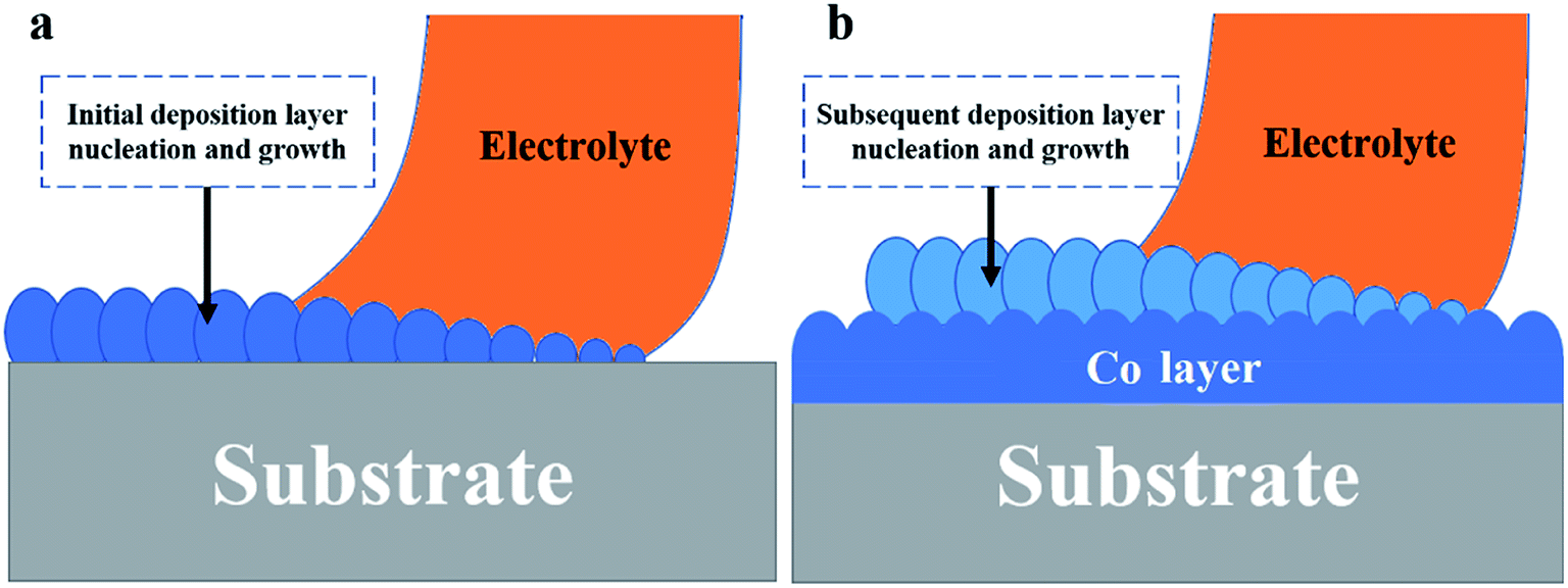
The Fig. 3 is a schematic diagram of a DCE deposition coating process, and the deposition method is a layer-by-layer stacking process. When the electrolyte droplets first contacted the substrate surface, a Co coating was electrodeposited on the surface of the steel substrate (Fig. 3a). Because the drip is continuously moved according to a set procedure, the time for Co crystals to grow on the surface of the substrate is limited. Because the electrodeposition area is limited to the droplet range, under a certain potential, the current density in the deposition area is higher, which will greatly increase the nucleation rate. At the same time, the limited deposition time in the unit area limits the growth of crystal nuclei, so the deposited layer is easy to form a fine grain structure. When the electrolyte drops pass through the same area again, the previously deposited Co coating becomes the substrate, and the subsequent electrodeposition is performed on the formed Co layer (Fig. 3b). Since the subsequent deposition is to deposit Co on the surface of the Co layer, the layers have good bonding properties and it is difficult to observe the layered structure. It is regrettable that since area-selective electrodeposition has more environmental parameters than traditional electrodeposition, such as the moving speed of the deposition area. Therefore, we cannot calculate and analyze its nucleation method through the traditional three-dimensional nucleation determination formula. However, the I–T curve data can intuitively reflect the changes in the coating deposition quality and the path program during the electrodeposition process in the selected area. This is more convenient for the existing selective electrodeposition technologies such as brush plating to rely on the observation and inspection of subsequent samples to evaluate the coating quality.
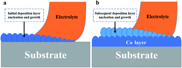 |
| | Fig. 3 Area-selective electrodeposition mechanism. (a) Initial deposition layer, (b) subsequent deposition layer. | |
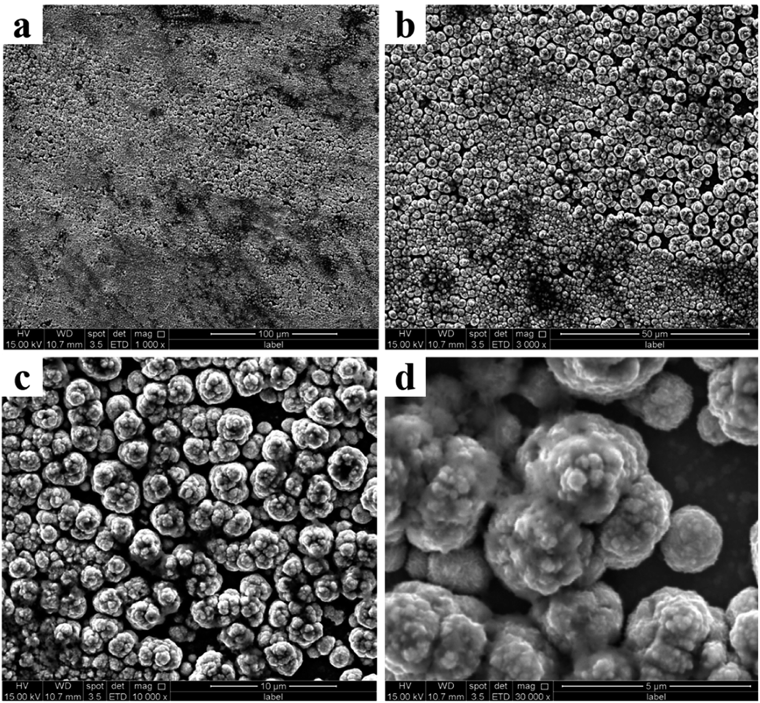
Observe the surface morphology of the sample by scanning electron microscope (SEM). A change can be observed in the microscopic surface morphology of the coatings deposited at different potentials (Fig. 4). The surface morphology of the coating is granular, and each particle is composed of many grains. Since electrodeposition is performed in a continuously moving region, the time for crystal nuclei to grow is limited. Since the electrodeposited region is constantly moving, the time for grain growth is limited, and it leaves the electrodeposition range before it is sufficiently grown. Therefore, under certain conditions of temperature and deposited time, the potential parameters are the main factors affecting grain growth and particle size on the surface of the coating. According to the I–T curve, the rise of the potential causes an increase in the current so that a higher potential value brings a higher nucleation and growth rate per unit time and area. Reflected on the surface of the coating, the surface particle size increases with increasing potential parameters.
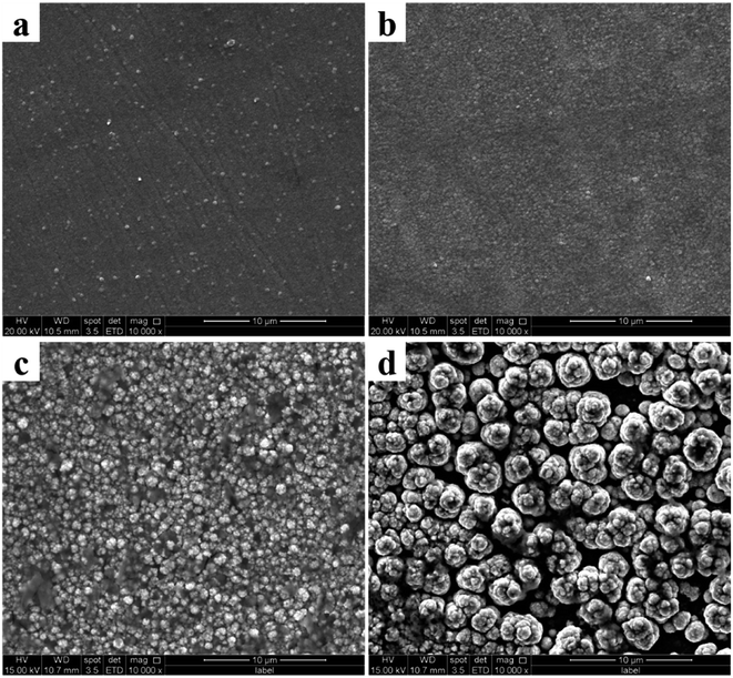 |
| | Fig. 4 The SEM images of Co coatings: (a) −2 V, (b) −2.5 V, (c) −3 V, and (d) −3.5 V. | |
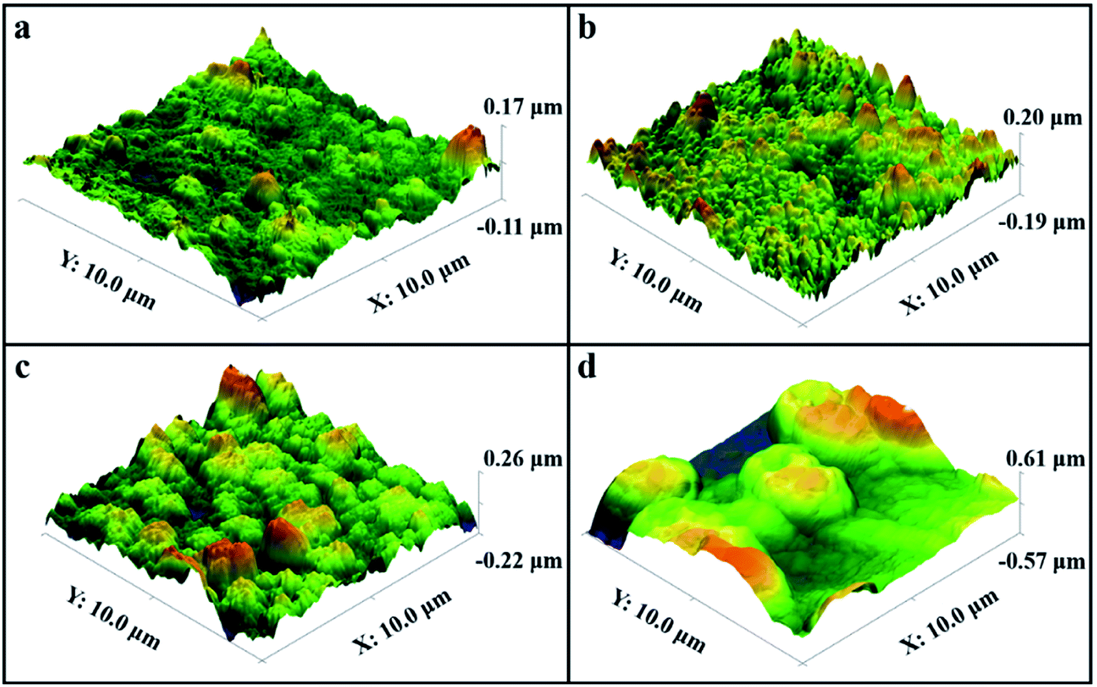
It can be seen from Fig. 4 that with the increase of the deposition potential, the particle size on the coating surface increase. To specifically observe the change in particle size, we performed AFM characterization on the coating surface prepared at different potential (Fig. 5). It can be proved from Fig. 5 that the particle size of the coating surface does increase with the increase of the potential, which is consistent with the result of Fig. 4. Therefore, we believe that the excessively high potential brings a larger potential difference during the electrodeposition process, which causes the speed of electrocrystallization to increase. Thus, Fig. 5d shows a larger particle structure than other samples. To verify whether the surface particle enlargement is a local phenomenon, we performed electron microscope observations (Fig. 6) at different ratios on the Co coating (Fig. 4d) surface prepared at −3.5 V. The increase in the size of the metal particles on the coating surface is not a local phenomenon, and mutual bonding between the metal particle structures is observed in Fig. 6d. Therefore, in the process of electrocrystallization by area-selective electrodeposition, metal particles grow up and merge into larger particle structures.
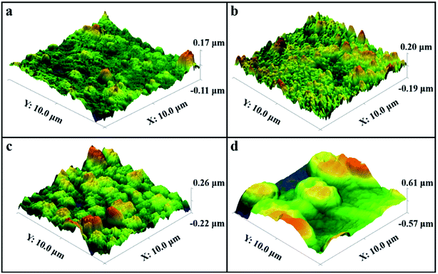 |
| | Fig. 5 The AFM images of Co coatings: (a) −2 V, (b) −2.5 V, (c) −3 V, and (d) −3.5 V. | |
 |
| | Fig. 6 Different scales morphology of cobalt coating surfaces prepared at −3.5 V. (a) 100 μm. (b) 50 μm. (c) 10 μm. (d) 5 μm. | |
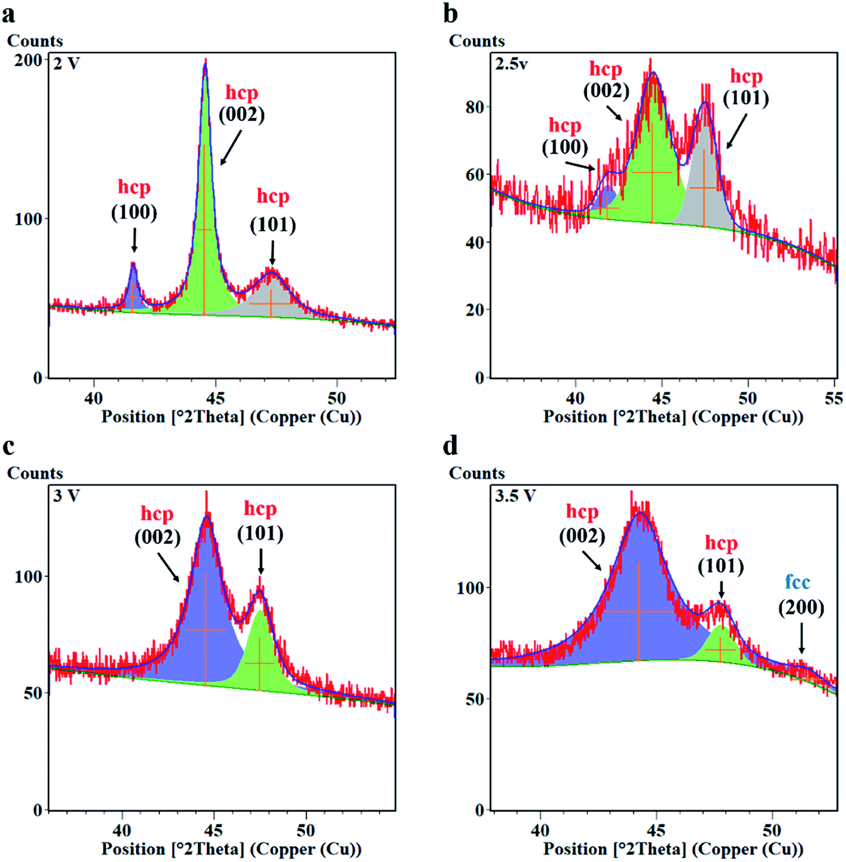
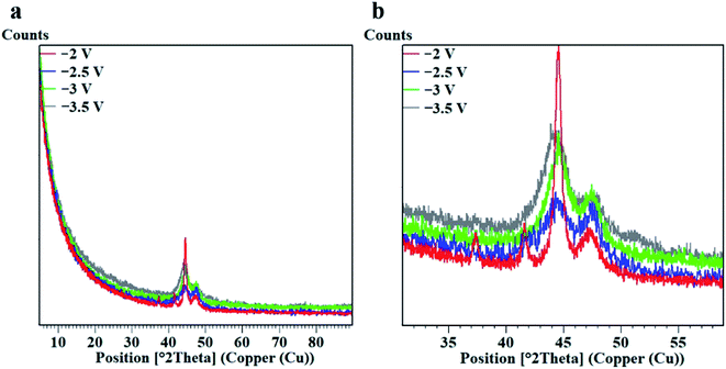
In the above analysis, we mentioned that in the process of area-selective electrodeposition, the limited nucleus growth time and the higher potential in the local area promote the generation of fine grains. Therefore, we performed XRD on Co coating samples under different potential analysis. The diffraction patterns of droplet contact electrodeposited Co coating are given in Fig. 7. As the potential value increases, the diffraction peak of Co gradually changes from three sharp peaks (−2 V) to two broad peaks (Fig. 7b). Observation of the electrodeposited Co coating shows a broad peak at 44.5°. By comparing the pdf card, we know that this peak can be attributed to the (002) plane of the hcp phase of Co. The Co coatings prepared under different parameters all have a main orientation in the (002) plane. The FWHM and peak height data of the Co coating (002) peak are shown in Table 4 by fitting analysis. As the potential rises, the full width at half maxima (FWHM) of (002) diffraction peak increases.
 |
| | Fig. 7 XRD peaks of the nanocrystalline Co coatings. (a) XRD overall figure, (b) XRD peak position enlarged figure. | |
Table 4 FWHM and peak height data of Co coatings (002) peak
| Sample |
2 V |
2.5 V |
3 V |
3.5 V |
| Peak height (cts) |
109.968 |
30.3165 |
24.319 |
45.3089 |
| FWHM (°Th.) |
0.615 |
1.604 |
2.136 |
3.006 |
Fig. 8 shows the XRD diffraction peak fit of Co under different potential values. When the potential parameters are −2, −2.5, and −3, the lattice structure of the Co coatings is hexagonal (hcp). When the potential parameter is −3.5 V, the lattice structure of the Co coating is still mainly hexagonal (hcp), and a small amount of cubic (fcc) appears at the same time. This is because the increase of the potential value causes the current density in the deposition area to rise, and thus causes the lattice type to change.22 It can be observed by fitting calculation that as the potential increases, the (100), (002), and (101) peaks of Co are broadened. When the potential is −2.5 V, the critical state of bimodal fusion can be observed (Fig. 8b). The potential further increased, the FWHM of the (002) diffraction peak was further broadened, and the (100) peak was no longer observed (Fig. 8c), while a small amount of lattice transition from hcp to fcc occurred. According to the Scherrer formula,23 D = Kλ/(β![[thin space (1/6-em)]](https://www.rsc.org/images/entities/char_2009.gif) cosθ), where K is the Scherrer constant (0.89), λ is the wavelength of the incoming X-ray (0.154056 nm), β is the full width at half maximum of the diffraction peak, θ is the Bragg diffraction angle, and D is the grain size. The grain size and microstrain of the Co coating prepared under different parameters are shown in Table 5. The grain size of the Co coating deposit calculated from the Scherrer method is nanoscale. In area-selective electrodeposition, potential parameters play an important role in grain refinement. Combined with the current–time curve (Fig. 1), the increase in potential causes a significant change in the deposition current. Under the condition of constant deposition area, the deposition current density is proportional to the potential parameter during electrodeposition, so the increase of potential value promotes atomic nucleation and growth. Because of the constant velocity movement of the electrodeposited region, the electrocrystallization time per unit area is limited, so the nucleation grains of the atomic deposit layer are not sufficiently grown to stop. This special electrocrystallization method easily forms nanocrystalline. When the deposition region returns to the surface of the deposited nanocrystalline Co layer again, since the crystal lattice and the deposition parameters are uniforms, the interlayer bonding property is good.
cosθ), where K is the Scherrer constant (0.89), λ is the wavelength of the incoming X-ray (0.154056 nm), β is the full width at half maximum of the diffraction peak, θ is the Bragg diffraction angle, and D is the grain size. The grain size and microstrain of the Co coating prepared under different parameters are shown in Table 5. The grain size of the Co coating deposit calculated from the Scherrer method is nanoscale. In area-selective electrodeposition, potential parameters play an important role in grain refinement. Combined with the current–time curve (Fig. 1), the increase in potential causes a significant change in the deposition current. Under the condition of constant deposition area, the deposition current density is proportional to the potential parameter during electrodeposition, so the increase of potential value promotes atomic nucleation and growth. Because of the constant velocity movement of the electrodeposited region, the electrocrystallization time per unit area is limited, so the nucleation grains of the atomic deposit layer are not sufficiently grown to stop. This special electrocrystallization method easily forms nanocrystalline. When the deposition region returns to the surface of the deposited nanocrystalline Co layer again, since the crystal lattice and the deposition parameters are uniforms, the interlayer bonding property is good.
 |
| | Fig. 8 Results of Co coatings XRD peak fitting. (a) −2 V, (b) −2.5 V, (c) −3 V, and (d) −3.5 V. | |
Table 5 Grain size and microstrain of coatings on (002) peak
| Sample |
2 V |
2.5 V |
3 V |
3.5 V |
| Grain size (Å) |
179.09 |
68.67 |
51.56 |
36.64 |
| Microstrain (%) |
0.946 |
3.144 |
3.442 |
4.821 |
The lattice strain also has a certain effect on the FWHM of the diffraction peak. If the diffraction peak width is only caused by lattice distortion, then ε = βn/4(tgθ), βn is only FWHM related to lattice strain (ε). The linear combination of Cauchy and Gaussian functions is widely used, that is the pseudo-Voigt function describes the diffraction peak shape formed by the grain size effect and the lattice strain effect.24 There have two expressions:25
| β = β + β′ = λ/(Dcosθ) + ε × 4tgθ, |
| β2 = β2 + βn2 = [λ/(Dcosθ)]2 + (ε × 4tgθ)2. |
Using this combination formula as a linear function can better adapt to the asymmetry of the diffraction peak shape. The parameters such as integral intensity, diffraction line position, full width at half maximum, and integral width are obtained by the least-squares method to calculate the strain value (Table 5). By calculating the grain size and lattice strain of the coating, it can be seen that the change rules of the two are the same as the grain reduction and lattice strain increase calculated by XRD. The grain size and microstrain were calculated at (002) peak, and they have a good correlation with FWHM where the crystallite size decreases with FWHM but micro-strain increases with FWHM. This conclusion is consistent with the conclusions of the existing research data.
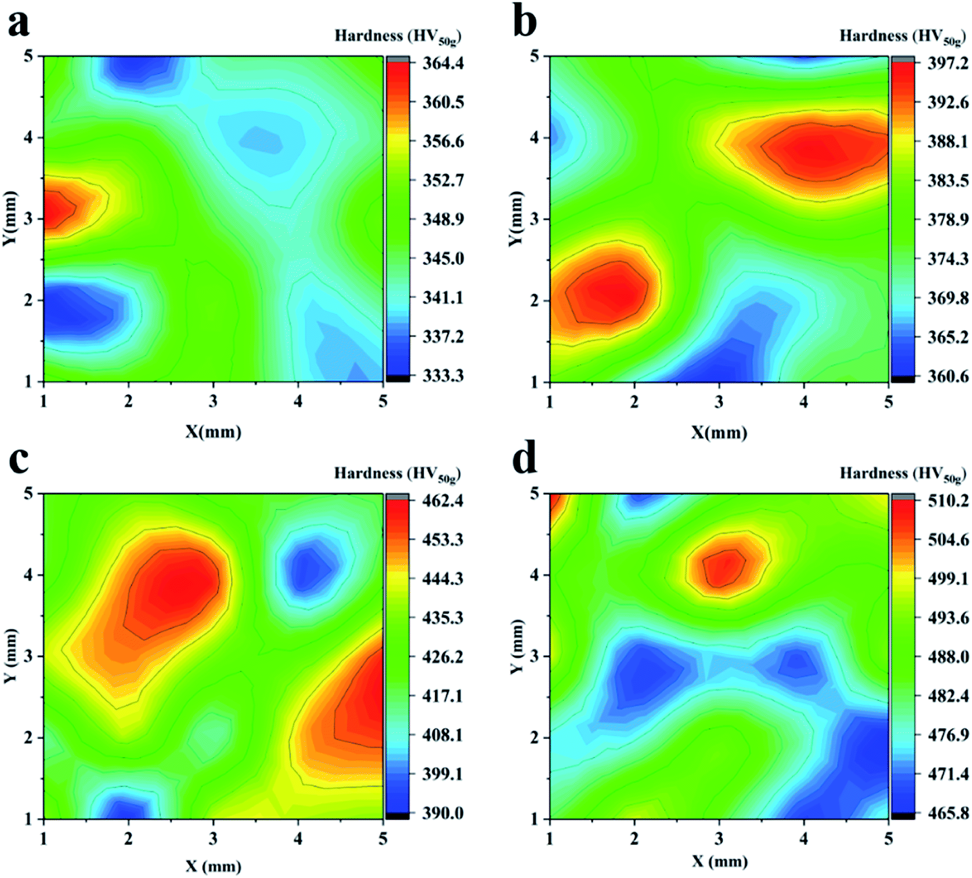
Through XRD analysis, we obtained grains and microstrain data of area-selective electrodeposited Co coatings, proving that they are nanocrystalline material (Table 5). Taking the −2 V parameter sample as an example, the average deposition current is 1.67 mA and the deposition area is 0.049 cm2 (area diameter 0.25 cm). The calculated current density of the −2 V sample was 34 mA cm−2. Comparing with Table 5, the nanocrystalline was successfully prepared by area-selective electrodeposition with lower current density and power. Existing research proves that in nanocrystalline materials, there is an internal relationship between the microstrain grain size changes, which is usually reflected in the physical properties of the material. We collected the microhardness of the Co coating surface prepared with different parameters, and obtained the microhardness distribution in the range of 5 × 5 mm on the coating center (Fig. 9). Generally, uneven hardness on the metal surface is normal. This is related to the structure of the coating and the substrate. In the steel substrate, there are usually various phase structures, such as austenite, martensite, etc. Different phases have different hardness, for example, the hardness of martensite is greater than that of austenite. The different hardness distribution of the steel substrate will affect the hardness of the coating surface to a certain extent. It is seen in Fig. 9 that as the potential parameter becomes larger, the degree of surface hardness fluctuation increases. This is due to the internal stress inside the Co coating. It can be proved from Table 5 that the smaller the crystal grains, the larger the micro-strain. Therefore, as the crystal grains are refined, the hardness value increases and the hardness fluctuation range increases. The strengthening effect brought by the grain refinement is obvious, but it is not the only factor affecting the hardness change. The XRD diffraction peaks (Fig. 8) show that the (002) crystal plane diffraction peaks of the Co coating increase with increasing potential. As the potential rise causes the current to increase (Fig. 2), the rate of electrocrystallization increases accordingly.26 Thus, the increase in electrocrystallization speed is also one of the factors that increase the hardness of the coating.
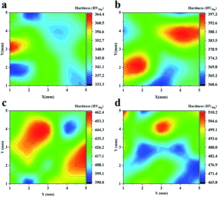 |
| | Fig. 9 The microhardness in the 5 × 5 mm area of the Co coatings surface. (a) −2 V, (b) −2.5 V, (c) −3 V, and (d) −3.5 V. | |
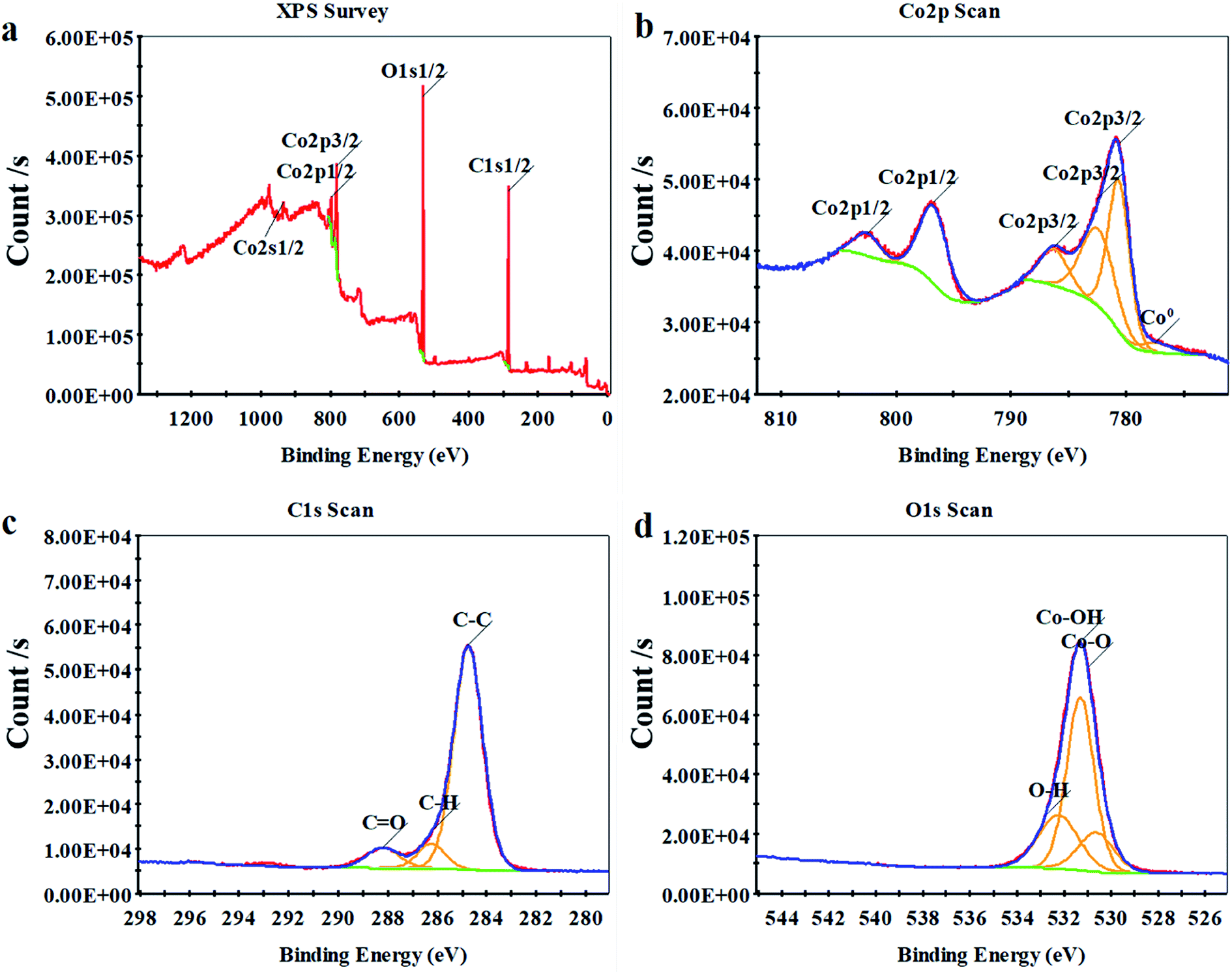
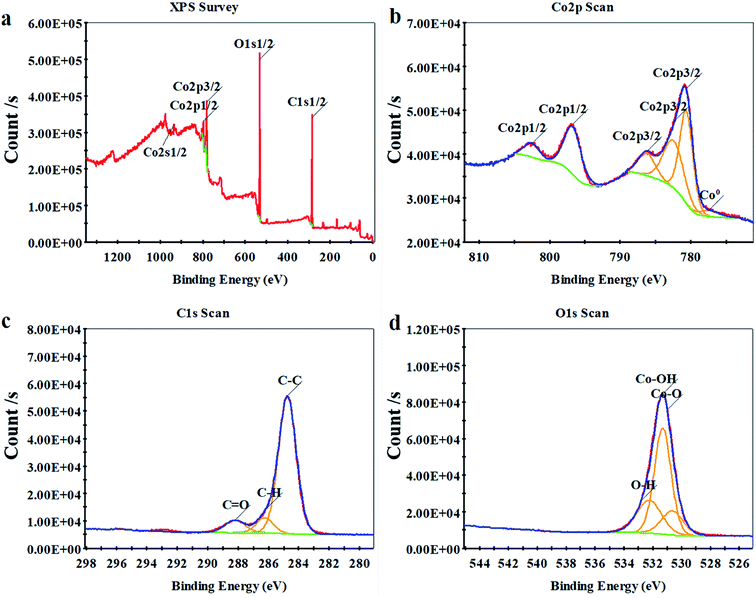
To study the coating element bond configuration and chemical composition, X-ray photoelectron spectroscopy (XPS) tests were performed on the coating surface (Fig. 10). All peaks in Fig. 10a are Co 2s1/2 (934.7 eV), Co 2p1/2 (797.1 eV), Co 2p3/2 (781.2 eV), O 1s1/2 (531.4 eV), C 1s1/2 (284.9 eV) and Co0 (777.5 eV). The Co0 peak at 777.5 eV represents Co metal, and its spin–orbit spacing is 14.8 eV. The peaks at 781.2 and 797.1 eV are due to the presence of Co2+ ions in the Co coating.27 Meanwhile, the XPS chart shows the presence of C and O on the Co-coated surface (Fig. 10a). Since the coating is oxidized at room temperature and absorbs impurities in the air, the XPS chart shows the presence of C and O on the surface of the Co coating (Fig. 10c).28–31 It can also be seen from the results of the C 1s spectral analysis of Table 6 that the C–C functional group accounts for 74.8% of the C-type functional group. It's can be further proved that the main source of C is the surface physical adsorption of pollutants. There have been studies to decompose the Co 2p peaks (including Co 2p3/2 and Co 2p1/2 peaks) into three main components: Co, Co–O and Co–OH.32 Therefore, three peaks of OH, Co–O, and Co–OH were used to fit the high-resolution peak of O 1s (Fig. 10d), and the fitted peak completely coincided with the original peak. The coating surface adsorbs water molecules in the atmosphere so that O–H peaks are shown in the O 1s scan. It can be seen from the fitting results that the coating oxide is mainly composed of Co–O and Co–OH. Because the binding energies of Co–O and Co–OH compounds are very close (779.6 and 780.5 eV), and the Co–O peaks are broad, the Co–O and Co–OH peaks overlap to a large extent.32 Existing research data indicate that there are two oxidation modes of Co coatings, which are considered to be double passivation film mechanisms.33 The oxide formed by the first oxidation method is mainly composed of CoO and Co(OH)2, and the oxide formed by the second oxidation method is mainly composed of CoOOH and Co3O4.
 |
| | Fig. 10 XPS spectra for the Co coating. (a) XPS survey, (b) Co 2p scan, (c) C 1s and (d) O 1s scan. | |
Table 6 Analysis results of C 1s spectra
| Name |
C–C |
C–H |
C–O |
Hydrophobic functional group content% |
| Peak BE (eV) |
284.76 |
286.13 |
288.20 |
74.8 |
| Atomic% |
3.35 |
0.37 |
0.76 |
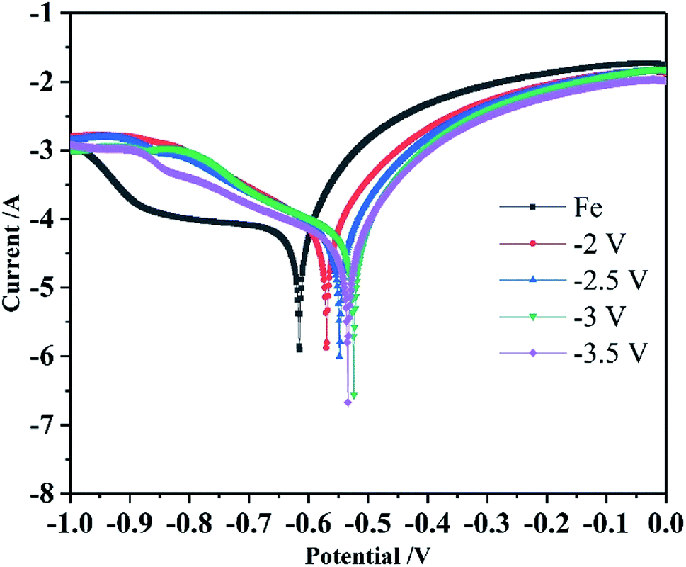
It is well known that nanocrystalline metals have obvious advantages over polycrystalline metals in many physical and mechanical properties. For their applications as protective coatings, corrosion resistance is also important. As shown in Fig. 11, the corrosion test of the prepared samples under different parameters in a 3.5 wt% NaCl solution was performed. The corrosion potential (Ecorr) and corrosion current density (Icorr) were calculated by extrapolation according to the potential polarization curve. The results are shown in Table 7. The results show that the nanocrystalline Co coating prepared by the area-selective electrodeposition method improves the corrosion resistance of the substrate, and the corrosion current decreases with the increase of the potential parameter. The increase of the potential parameter causes the grain size to decrease and the grain boundary density to increase. The electrochemical corrosion and passivation behavior of the nanocrystalline Co coating is a diffusion control mechanism. The higher grain boundary density in the nanocrystalline material strongly affects the corrosion behavior of the nanocrystalline material. In the NaCl solution, due to the higher grain boundary density in the nanocrystalline material, a continuous protective passivation film can be quickly formed. Therefore, in these corrosive media, it is desirable to effectively enhance the nanocrystalline Co coating without losing its high corrosion resistance. Therefore, the controversial experimental results of nanocrystalline Co coatings in different corrosion media can be reasonably explained by the positive and negative effects of the high-density grain boundary network.33
 |
| | Fig. 11 Tafel curves of the Co coatings. | |
Table 7 The corrosion data of Co coatings
| Sample |
Anodic Tafel slope (1/V) |
Cathodic Tafel slope (1/V) |
Icorr (A cm−2) |
Ecorr (V) |
| Fe |
9.669 |
1.103 |
1.123 × 10⁻⁴ |
−0.615 |
| −2 V |
8.944 |
4.831 |
9.291 × 10⁻⁵ |
−0.570 |
| −2.5 V |
9.366 |
4.203 |
7.857 × 10⁻⁵ |
−0.548 |
| −3 V |
9.503 |
3.794 |
7.568 × 10⁻⁵ |
−0.524 |
| −3.5 V |
9.494 |
3.603 |
5.824 × 10⁻⁵ |
−0.534 |
4 Conclusion
In this paper, nanocrystalline Co coatings were successfully produced by area-selective electrodeposition. The control of the program makes it possible to draw a corresponding coating on a circular substrate. Control program and deposition patterns have a direct impact on coating organization, morphology, and quality. According to different deposition patterns, the simplest and most optimized procedure can directly affect the microstructure and deposition efficiency of the deposited coating. Meanwhile, the current–time curve successfully reflects the changes of the electrodeposition process in the selected area. The surface microstructure of the nanocrystalline Co coating is granular. In the process of electrodeposition, the current density in the deposition area is not only concentrated, but the grain growth is also restricted. This unique deposition mode facilitates the production of nanocrystals. The movement of the electrodeposited region brings about intermittent nucleation mode, so that the intermittent deposition of Co ions forms hcp (1 0 0), (0 0 2) and (1 0 1) textures in the coating, and the grain size decreases as the potential increases. The crystal face of the Co coatings is mainly hcp (002). With the deposition of nanocrystalline Co coatings, the corrosion resistance of the substrate is improved. Through analysis and calculation, as the deposition potential increases, the Co coating grain becomes smaller and the corrosion resistance increases. Compared with traditional electrodeposition, not only the deposition potential, but also the control program and deposition pattern affect the phase structure, morphology, and corrosion resistance of the prepared coating. By analyzing the phases in the coating, the nanocrystalline Co coatings prepared in the range of −2 to −3.5 V are mainly hcp (1 0 0), (0 0 2) and (1 0 1) crystal planes. In the −3.5 V parameter, the coating structure appeared fcc (200) crystal-plane. With the increase of the potential parameter, the grain size of the Co coating decreases and the microstrain increases. The hardness and corrosiveness of the coatings were tested, and the results proved that the area-selective electrodeposition Co coating improved the surface properties of the substrate.
Conflicts of interest
There are no conflicts to declare.
References
- M. K. Das, R. Li, J. Qin, X. Zhang, K. Das, A. Thueploy, S. Limpanart, Y. Boonyongmaneerat, M. Ma and R. Liu, Surf. Coat. Technol., 2017, 309, 337–343 CrossRef CAS.
- S. Tjong and H. Chen, Mater. Sci. Eng., R, 2004, 45, 1–88 CrossRef.
- F. Li, T. Liu, J. Zhang, S. Shuang, Q. Wang, A. Wang, J. Wang and Y. Yang, Mater. Today, 2019, 4, 100027 CrossRef.
- F. Nasirpouri, in Electrodeposition of Nanostructured Materials, Springer, 2017, pp. 261–288 Search PubMed.
- J.-s. Meng, G. Jin and X.-p. Shi, Appl. Surf. Sci., 2018, 431, 135–142 CrossRef CAS.
- D. Landolt, Electrochim. Acta, 1994, 39, 1075–1090 CrossRef CAS.
- O. Bayat, V. Abouei, H. Sabet and A. Kiasati, Prot. Met. Phys. Chem. Surf., 2018, 54, 63–70 CrossRef CAS.
- K. M. Hyie, N. A. Resali, W. N. R. Abdullah and W. T. Chong, Procedia Eng., 2012, 41, 1627–1633 CrossRef CAS.
- I. Kharmachi, L. Dhouibi, P. Berot and M. Rezrazi, J. Mater. Environ. Sci., 2015, 6, 1807–1812 CAS.
- D. P. Weston, P. H. Shipway and S. J. Harris, Wear, 2009, 267(5–8), 934–943 CrossRef CAS.
- F. Su, C. Liu, Q. Zuo, P. Huang and M. Miao, Mater. Chem. Phys., 2013, 139, 663–673 CrossRef CAS.
- A. Aledresse and A. M. Alfantazi, J. Mater. Sci., 2004, 39, 1523–1526 CrossRef CAS.
- A. A. Karimpoor and U. Erb, Phys. Status Solidi A, 2006, 203, 1265–1270 CrossRef CAS.
- D. Facchini, N. Mahalanobis, F. Gonzalez and G. Palumbo, 2009.
- G. Qiao, T. Jing, F. Xiao and Y. Gao, Chin. J. Mater. Res., 2004, 139, 663–673 Search PubMed.
- G. Jin, D. Zhang, M. Liu, X. Cui, E. Liu, Q. Song, C. Yuan, X. Wen and Y. Fang, J. Alloys Compd., 2019, 801, 40–48 CrossRef CAS.
- L. Shen, M. Xu, W. Jiang, M. Qiu, M. Fan, G. Ji and Z. Tian, Appl. Surf. Sci., 2019, 489, 25–33 CrossRef CAS.
- M. Manov and T. Kalinov, 2019.
- M. Kang, Y. Zhang and H. Li, Procedia CIRP, 2018, 68, 221–226 CrossRef.
- F. Zhang, Z. Yao, O. Moliar, X. Tao and C. Yang, J. Alloys Compd., 2020, 153785 CrossRef CAS.
- F. Zhang, Z. Yao, O. Moliar, X. Tao and C. Yang, Mater. Res. Express, 2019, 6, 106411 CrossRef CAS.
- M. S. Bhuiyan, B. Taylor, M. Paranthaman, J. R. Thompson and J. Sinclair, J. Mater. Sci., 2008, 43, 1644–1649 CrossRef CAS.
- U. Holzwarth and N. Gibson, Nat. Nanotechnol., 2011, 6(9), 534 CrossRef CAS PubMed.
- H. Wang and J. Zhou, J. Appl. Crystallogr., 2005, 38, 830–832 CrossRef CAS.
- A. R. Bushroa, R. Rahbari, H. H. Masjuki and M. R. Muhamad, Vacuum, 2012, 86, 1107–1112 CrossRef CAS.
- J.-X. Kang, W.-Z. Zhao and G.-F. Zhang, Surf. Coat. Technol., 2009, 203, 1815–1818 CrossRef CAS.
- P. Bera, H. Seenivasan, K. Rajam and V. W. Grips, Mater. Lett., 2012, 76, 103–105 CrossRef CAS.
- S. Devillers, A. Hennart, J. Delhalle and Z. Mekhalif, Langmuir, 2011, 27, 14849–14860 CrossRef CAS PubMed.
- D. Phase, R. J. Choudhary, V. Ganesan, V. R. Reddy, A. Gupta, N. Selvi, S. Kulkarni and S. Ogale, Solid State Commun., 2009, 149, 277–280 CrossRef CAS.
- W. Kozłowski, I. Piwoński, M. Zieliński, E. Miękoś, K. Polański, W. Szmaja and M. Cichomski, Appl. Phys. A: Mater. Sci. Process., 2015, 120, 155–160 CrossRef.
- W. Kozłowski, J. Balcerski and W. Szmaja, J. Magn. Magn. Mater., 2017, 423, 256–261 CrossRef.
- H. A. E. Hagelin-Weaver, G. B. Hoflund, D. M. Minahan and G. N. Salaita, Appl. Surf. Sci., 2004, 235, 420–448 CrossRef CAS.
- L. Wang, Y. Lin, Z. Zeng, W. Liu, Q. Xue, L. Hu and J. Zhang, Electrochim. Acta, 2007, 52, 4342–4350 CrossRef CAS.
|
| This journal is © The Royal Society of Chemistry 2020 |
Click here to see how this site uses Cookies. View our privacy policy here. 
 Open Access Article
 This Open Access Article is licensed under a Creative Commons Attribution-Non Commercial 3.0 Unported Licence
 ab,
Shasha Zhangab,
Oleksandr Moliarab and
Zelei Zhanga
ab,
Shasha Zhangab,
Oleksandr Moliarab and
Zelei Zhanga