
 Open Access Article
 This Open Access Article is licensed under a Creative Commons Attribution-Non Commercial 3.0 Unported Licence
Optimized Ni1−xAlxO hole transport layer for silicon solar cells
S. Halilov†
 *a,
M. L. Belayneha,
M. A. Hossainb,
A. A. Abdallaha,
B. Hoexb and
S. N. Rashkeeva
*a,
M. L. Belayneha,
M. A. Hossainb,
A. A. Abdallaha,
B. Hoexb and
S. N. Rashkeeva
aQatar Environment and Energy Research Institute (QEERI), Doha, Qatar. E-mail: shalilov@hbku.edu.qa
bSchool of Photovoltaic and Renewable Energy Engineering, University of New South Wales, Sydney, New South Wales, Australia
First published on 11th June 2020
Abstract
NiO alloyed with aluminum, Ni1−xAlxO, is analyzed in terms of its stoichiometry, electronic and transport properties, as well as interfacial band alignment with Si to evaluate its potential use as a hole transport layer (HTL) in p–i–n type solar cells. The analysis is based on component material and slab structural simulations, as well as simulated and measured angle-resolved valence-band photoemission spectroscopy (PES) data, in order to reveal the best suitable stoichiometry. It is concluded that the ionization energy from the highest occupied states tends to increase with Al content as the simulated work function grows from 4.1 eV for pure NiO to 4.7 eV for heavily alloyed Al0.50Ni0.50O. The electronic structure as a function of the interface design between crystalline silicon and the transport layer is used to assess the band lineup and its correlation with the discontinuity of the affinities. The affinity rule is tested by evaluating the workfunctions of the component layers and justified best for a particular Ni-enriched interface design. Technology Computer-Aided Design (TCAD) device simulations show, that the band offset between oxide and crystalline silicon remains within the range of values to sustain a staggering alignment – a condition suitable for effective charge separation, similar to a situation in a tunneling diode. The self-energy of the hole carriers is estimated by contrasting simulated and measured photoemission data, which in the case of non-annealed Al-rich samples is shown to be an order of magnitude higher due to the disorder effects. The work functions derived from the measured PES data for the epitaxially grown oxide films with nearly identical alloy stoichiometry correlate well with the simulated values. The findings suggest that the optimal HTL is formed by starting with a pure Ni layer, followed by a graded doping AlxNi1−xO, with x high at contact/oxide interface and low at the oxide/semiconductor.
1 Introduction
Metal oxides have their functionality determined by a relatively large set of parameters such as lattice, spin, charge and orbital degrees of freedom. Alloying NiO with Cu was shown to increase the hole dopant level associated with Cu+ sites and a conversion efficiency as high as 6.3% was reported for a heterojunction solar cell featuring Cu doped NiO as an HTL.1 Epitaxially grown semiconductors such as Co-doped NiO with suitable electron affinity, band gap and near-the-top valence band density of states has a high potential to serve as charge-selective transport layers in perovskite photovoltaic (PV) cells with distributed charge collectors,2 on one hand, and as highly effective electrocatalysts for hydrogen evolution reaction with activity similar to platinum,3 on the other hand. NiO alloyed with Zn and Atomic Layer Deposition (ALD)-grown on c-Si demonstrates a low contact resistance of 1.5 mΩ cm2, having a high potential to serve as a HTL.4It is also well known that passivation of the defect states (e.g. dangling bonds) at the interface with the absorber, such as c-Si and halide perovskite, is another factor adding to the advantage of inserting a thin layer of the oxide between metallic contacts and the absorber.5 However, in practice that a quality transport layer has to fulfill a set of conditions such as a band lineup appropriate for high charge selectivity, reduced contact Schottky barrier and low ohmic resistance, and in lesser extend higher carrier mobility. Here the main focus is on the effects of local stoichiometry rather than bulk characteristics on the targeted physical properties of the alloy oxide as a part of heterostructure in the pertinent PV cell. Without extra measures, the highest conversion efficiency in halide perovskite PV cells doesn't get better than 15% using optimised pristine NiOx.6 In another perovskite-based example, efficient NiOx HTL was fabricated by oxidation of metal Ni film, which delivers between 12 and 16% conversion efficiency depending on the annealing conditions.7 The high impact of the growth morphology on the interface band alignment, defect structure and carrier mobility indicates on even more options offered by alloying NiO with Al in order to further optimize the PV cell based on c-Si absorber – main subject of the current research.
We report our studies of the surface electronic properties of NiO and its alloys with Al using plane-wave based structural relaxation followed by the multiple-scattering simulations of the photo-excited electrons and holes. Particular focus is on the band alignment between the oxide layer and Si substrate in the context of the optimized carrier transport material used in p–i–n silicon PV cells. The resistive properties between external Al contact and AlxNi1−xO oxide strongly depend on the type and concentration of the interface impurities. These impurities affect the interface defect density Dit, which can release or capture charge and thus alter the surface potential ϕ0. All these factors become the primary mechanism of the Fermi level pinning and determine the Schottky barrier height roughly as ϕSB ∼ 1/2(EG − ϕ0) for high enough Dit, and would follow the difference between the work functions EW, i.e. ϕSB ∼ ϕW,met − ϕW,ox, in the limit of low Dit, with EG being the band gap in the oxide.8 Since ϕ0 quantifies the lower acceptor states from the higher donor states within the oxide gap, a higher acceptor concentration generally leads to a higher ϕ0 and thus to lower barrier ϕSB. As the simulations show in the case of AlxNi1−xO, a higher Al content implies higher acceptor concentration, which therefore might lead to a higher surface potential and hence smaller Schottky barrier and diminished Fermi energy pinning, – a favorable situation for having a better ohmic contact. Moreover, as a general rule of thumb, situations when ϕW,met < ϕW,ox in case of metal–p-type semiconductor junction are more beneficial for having a better ohmic contact, since the adverse effect of the space charge effect of the impurity states in the gap on the band alignment is minimized. On the other hand, the simulations demonstrate a significant dependence of the work function of the oxide on the Al content, with a substantial impact on the band alignment between the oxide and Si, which is the main focus of this work.
In order to reveal the effect of alloying between NiO and Al on the selective carrier transport properties, the surface and bulk electronic structures of AlxNi1−xO were also investigated in terms of its angular resolved photoemission spectrum (ARPES) response.
The approach allows a direct comparison between the calculated photocurrent and angle-resolved photoemission (PE) measurements. Previously, similar analysis of (001) LaCoO3 data offered direct evidence of the surface stoichiometry and the presence of surface magnetism as deduced from the PE measurements and simulations.9
The paper is organized as follows. Results of surface relaxation of the pristine NiO and AlNiO alloys are presented in Section 2. The work function for various stoichiometries is derived from the electrostatic potential averaged over the slab and the vacuum regions. The photoemission spectra in UV range of the photon energies were simulated within the framework of the layer Green function multiple scattering formalism.10 By contrasting theoretical data with those recorded in the angle resolved photocurrent measurements, important features of the carriers such as lifetime and relative changes in the effective density of states upon alloying were estimated. Foundations of the so-called one-step photoemission theory are briefly discussed in Section 3, followed by Sections 4 and 5, where the PE method was applied to pure NiO and its alloy with Al, respectively. Surface magnetism, effective carrier lifetime and effective density of states are considered in details. The paper is summarized in Section 6.
2 Relaxation of AlxNiyO/c-Si heterostructure: derivation of band lineup
The affinity rule is known to be a simple and widely used in device simulations approach to integrate a certain band lineup at the heterojunction interfaces in order to capture the main features of the carrier transport.11 It is based on the using the values of the affinity discontinuity at an abrupt junction between nondegenerated semiconductors for extrapolating band diagram across the junction. For example, using 4.05 eV for affinities of c-Si with a gap of 1.12 eV and 1.8 eV of nearly stoichiometric NiO (ref. 12) with a gap of 3.6 eV results in 0.27 eV for the valence band offset, implying a barrier for holes and defying the purpose of NiO as an HTL. We start here with the derivation of the work function for the constituent materials followed with the actual interfacial structure and band lineup in order to adjust the affinity rule and facilitate the device simulation.2.1 Case of isolated constituent materials
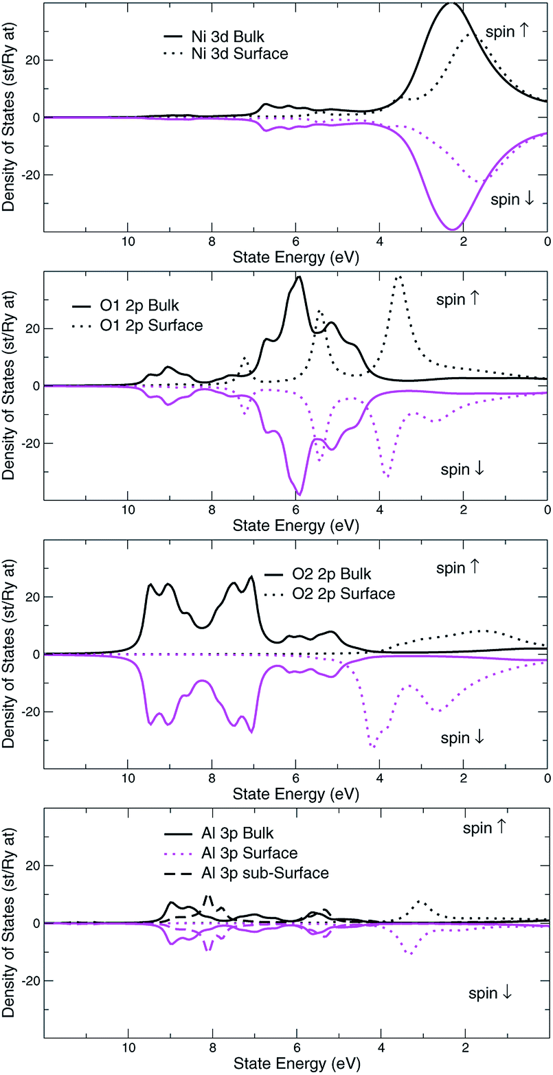
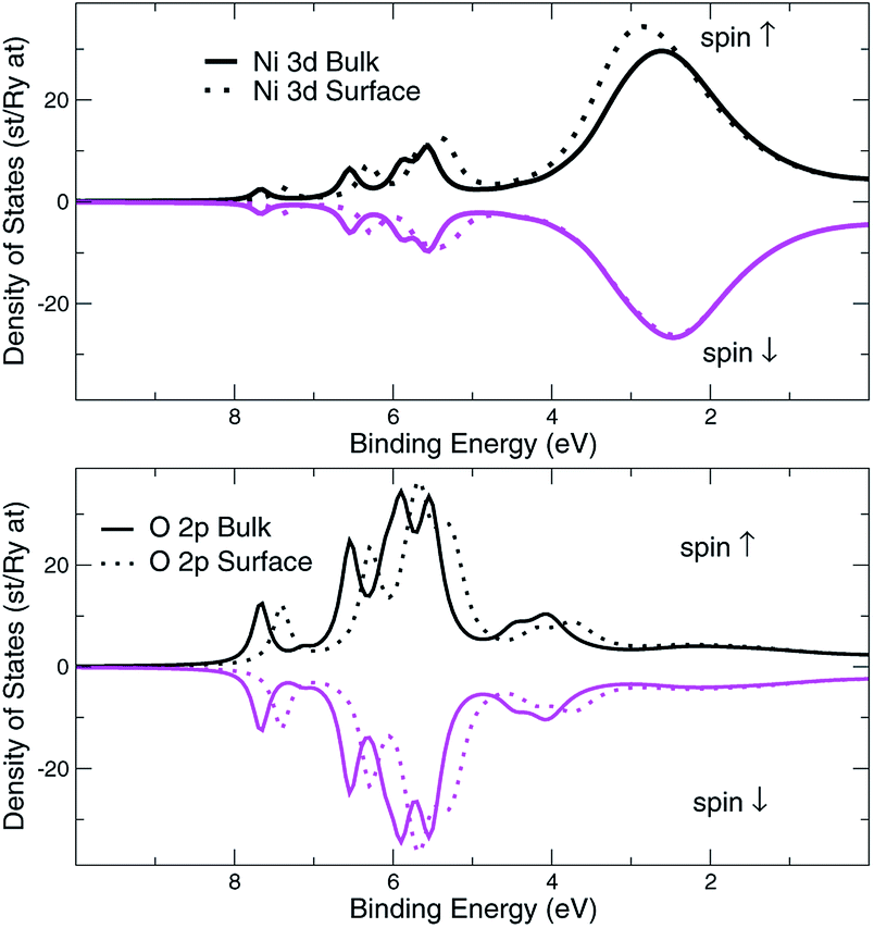
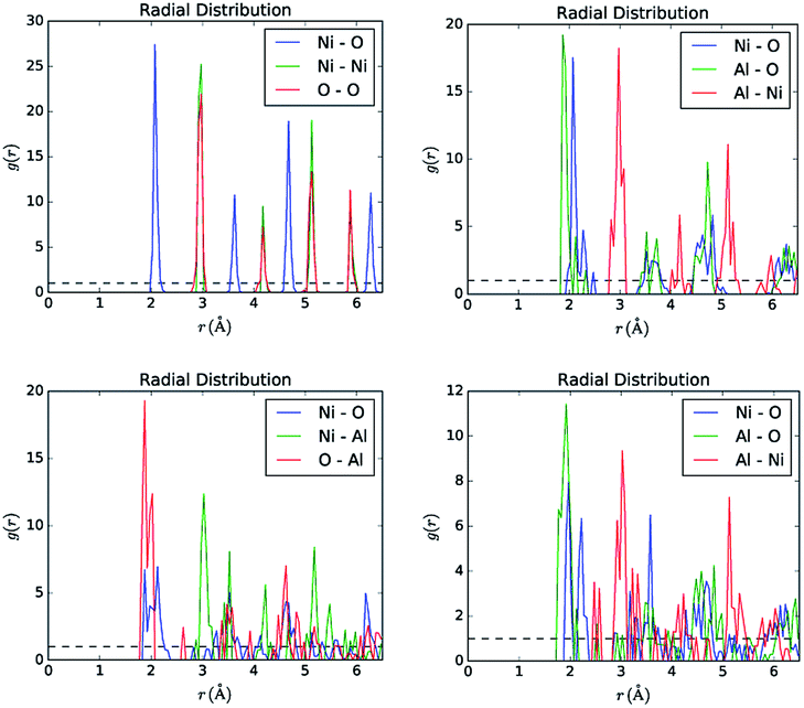
The structural surface relaxation of NiO was obtained by using an orthorhombic slab 4 stoichiometric units thick along the normal to the surface with 2 × 2 × 4 surface unit cell which accommodates antiferromagnetic ordering of AFM II type, as well as a wide range of surface defects concentration due to non-stoichiometric composition on the top. The approach involves the plane wave basis as implemented within VASP-PAW code.13 The van der Waals interaction is included at all stages of the simulations. The size of the vacuum was set to 4 stoichiometric units along the stacking direction, i.e. around 16.8 Å and was proven as large enough to avoid the spurious solutions.The Al0.5Ni0.5O (001) alloy was simulated within 2 × 2 × 6 supercell, with 2 × 2 in-plane cells used for better spin relaxation, followed by vacuum, the relaxed structure is shown in Fig. 1. Due to shorter 1.9 Å bonds between Al and O versus 2.2 Å for Ni–O bonds, the surface-region slab undergoes a substantial relaxation, with Al atoms dipped toward the bulk. There is some 0.3 μB spin polarization on the surface Ni sites, and relatively large 1.7 μB on the surface low-charge O sites coupled to the surface Al atoms, designated as O2 sites in Fig. 2. These trends are to be compared to the case of pristine NiO. The layer-resolved density of states (LDOS) for AFM II configuration of NiO is demonstrated in Fig. 3, where a considerable distinction between surface and bulk states of Ni is to be noticed. The distinction is due to the differences in the local magnetic polarization, with about 1.2 μB on the surface versus 0.6 μB in the bulk. In case of Al0.5Ni0.5O, the oxygen 2p states are now more dispersed over binding energy scale, dominating the region between 8 and 3 eV. Thus, the Al atoms push away the O states from the Fermi level toward higher binding energies and contribute to the states within the original gap, confirming the trend towards higher metallicity at higher Al concentration. This overcompensating trend toward higher donor states was emphasized earlier in the context of electrochromic films of AlNiO,14 where the concentration of Al was as high as 10%. In our case of 50% the trend is obviously even stronger. However, p-type doping mechanism is dominating in the limit of lower 2.5% Al content confirmed earlier15 in DFT simulations. One quick conclusion is that substitutional Al serves as p-dopant at Al concentrations as low as few percents and becomes overcompensated by donor states at higher Al content. In the bulk, the local moment on Ni sites is significantly reduced as compared to the case of the pristine NiO. The reasoning behind is likely due to larger intersite exchange interaction in presence of Al ions thanks to itinerant electrons, which competes with the onsite exchange and leads to diminishing the associated local Ni-centered spin moment. A parallel in trends can be made to Ni1−xAlx alloys where it was found that increase of Al concentration from 0.22 to 0.28 leads to a substantial drop in Ni-centered moment from 0.40 bohr to 0.18 bohr magnetons,16 which correlates with the density of states at the Fermi level.
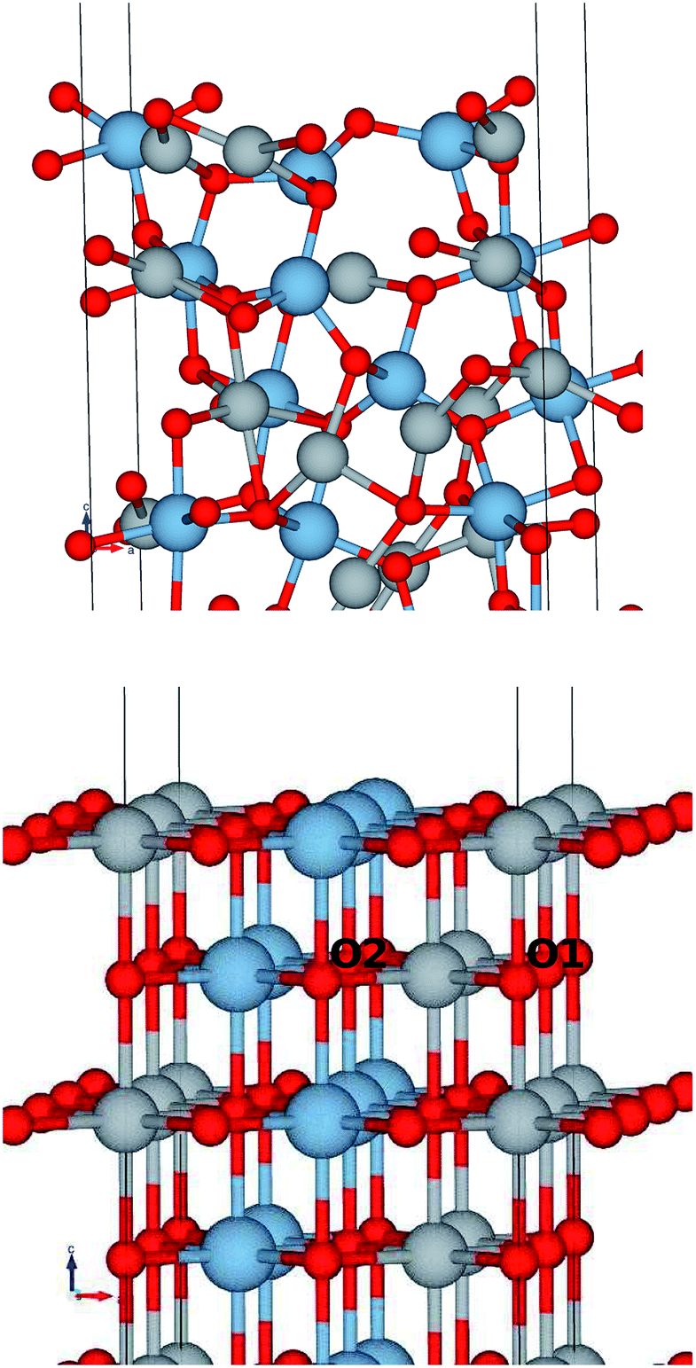 | ||
| Fig. 1 Ball and stick model of the Al0.5Ni0.5O (001), near surface region. (Top panel) Fully relaxed, (Bottom) initial structure before relaxation. Small red balls stand for oxygen, large blue balls for Al, and gray balls for Ni. | ||
 | ||
| Fig. 2 Al0.5Ni0.5O compound, surface and bulk layer resolved density of d-states, Ni site, p-states, O sites, and p-states, Al site. Two different O sites are shown to emphasize the very distinct spin states. | ||
 | ||
| Fig. 3 NiO AFMII, surface and bulk layer resolved density of d-states, Ni site, and p-states, O site. Spin majority and spin minority states are in upper and lower halves, respectively. | ||
Also, O1 and O2 atoms even in the bulk have different coordination: O1 is coordinated by 4 Ni and 2 Al atoms, whereas O2 sees 2 Ni and 4 Al atoms as nearest neighbors.
That would explain a significant effect of higher Al coordination on O states, shifting O2 states toward higher binding energies by approximately 2 eV as compared to those of O1 atoms. Overall, the valence band states, which are of mostly 2p character, were broadened by 2 eV as a result of alloying with Al. These conclusions are easy to infer by comparing the electronic structure of the alloy to the case of pristine NiO, shown in Fig. 3.
In order to extract the work function, the method of partial relaxation was applied here to a slab/vacuum configuration where the bottom and top layers are forced to stay identical during the relaxation process. This was used to eliminate the electrostatic bias across the slab, which also flattens the vacuum potential and thus allows for easy extraction of the work function as a difference between the vacuum level and the Fermi energy, the latter defined as the energy of the topmost occupied state. The quality of ordering can easily be assessed from the pair distribution function, illustrated in Fig. 4. Obviously, the correlation length drops below 3 Å as oxygen atoms get re-distributed swarming more around Al atoms. The coordination around Al is close to Al2O3 stoichiometry, when the concentration of Al increased to above 25%. Besides, a higher Al content leads to a contamination of the band gap with states close not only to the top of the valence band, but also to the bottom of the conduction band. Thus the introduction of Al results in both p- and n-doping, which, on account of the vacant Ni serving as the major source of holes, is still suitable for the layer to serve as an HTL at the junction with c-Si thanks to the oxide's potential barrier for electrons. In the case of pristine NiO, the long-range ordering is still pretty high as compared to the case of Al alloys, which however is not the case for ALD grown NiO, as will be seen from the UPS analysis. That level of disorder impacts the mean collision time and hence mobility, as well as life time due to increased concentration of the recombination centers, – both are expected to be minor factors for the conversion efficiency if the oxide is sufficiently thin.
 | ||
| Fig. 4 Pair distribution function for NiO and samples Q, R, S, as derived from the partially relaxed slab simulations. | ||
The simulated work function values for NiO and its Al alloys, Al0.08Ni0.92O (S1), Al0.16Ni0.84O (S2) and Al0.25Ni0.75O (S3), along with ALD-grown samples Al0.25Ni0.75O (Q), Al0.33Ni0.67O (R), Al0.50Ni0.50O (S), are summarized in Table 1, where GGA is combined with a local Coulomb repulsion U = 6 eV for the Hubbard parameter. The alloys S1, S2, S3 can roughly be considered as theoretical counterparts of the ALD grown Q, R, S samples, respectively.
| Sample | EW, eV (theory) | EW, eV (UPS data) |
|---|---|---|
| Si | 4.53 | 4.6–4.85 |
| NiO | 4.07 | 4.51 |
| S1, Q | 4.12 (S1) | 4.68 (Q) |
| S2, R | 4.44 (S2) | 4.87 (R) |
| S3, S | 4.61 (S3) | 4.89 (S) |
2.2 Case of AlxNiyO/c-Si slab
In order to address the issues involved in band offset derivation and see whether the situation is bulk or rather interface specific,17 it is natural to have both constituent component materials in the same simulation. By doing so in a framework of a slab, one potentially eliminates the problem of the individual reference points, however a detailed analysis of the average potential across the interface is required to assess the issues related to the finite thickness of the slab.18 To this point, the Si-(111) surface was considered as more suitable for building an ordered interface with NiO due to a more optimal lattice matching, thus excluding effects of strain on the band lineup and the energy gap. Also, anticipating a higher work function for Al-enriched NiO which is detrimental for the charge selectivity, the Al-alloying was implemented a few layers away from the c-Si interface. Besides, as it turns out, adding Al to the interface with c-Si leads to a higher level of structural disorder upon relaxation. The system in question was designed as follows: 4 layers of c-Si with a (111) orientation as the stacking direction, followed by 3 layers NiO(111) with an O-rich interface, and three more cases of Al substituting Ni in the topmost NiO layer, in three different stoichiometries. The work function is generally known to depend on the type of the surface face, but in case of a high level of disorder the effect is expected to be accordingly smeared and so obtained results are considered as universally applicable to other surfaces, particularly to (001) as more practical as well. An example of the relaxed NiO/c-Si slab with O-rich interface is illustrated in Fig. 5. Another simulated slab stoichiometry is S1/c-Si (not shown). | ||
| Fig. 5 Ball and stick model of relaxed NiO/c-Si(111), O-rich interface region. Small red balls stand for O, blue balls are for Si, gray balls are for Ni. | ||
Note that EW for NiO(111) is higher than that for NiO(001), which usually is expected for the direction of higher packing factor. With that in mind, the values for S1, S2, S3 can be scaled down by roughly 0.8 eV for the (001) orientation, what would bring the numbers close to those reported in Table 1. The results of the slab simulations are discussed in the next subsection, where they are used along with the isolated materials data in order to show how to adjust the affinity rule and provide the right band lineup in the evaluation of the pertinent device efficiency.
2.3 Effect of the interface dipole on the band lineup and optimized stoichiometry
A self-consistent surface or interface approach is a more accurate and reliable method for establishing affinity discontinuities and work functions. There is a certain range of the band alignment discontinuity suitable for transport in p–i–n PV cells19 in general. Fig. 6 illustrates the device-simulated conversion efficiency and fill factor versus the variations of EV(Si)–EV(NiO), for a c-Si/NiO PV cell with distributed back contact and NiO as a back hole transport layer. A quick list of the TCAD parameters is as follows, from illuminated side towards the back contact: 200 nm of c-Si, with its top 5 nm layer dopped with Nd = 1020 cm−3 and the rest with Np = 1016 cm−3, followed by 2 nm thick layer of NiO dopped with Np = 1020 cm−3 and attached to the back contact. The ordinary physical models such as defect-concentration-dependent Shockley–Read–Hall (SRH) and Auger mechanisms for recombination, as well as thermionic emission and tunneling around the oxide and contact, have been included to account for major recombination mechanisms. No further TCAD details are provided here in order to stay within the scope of the work and focus instead on main trends. The curves in Fig. 6 clearly emphasize the edge-like behavior of the performance when the valence states of NiO drop by more than 0.1 eV below the valence states of c-Si (negative band offset in Fig. 6). The sudden drop of the fill factor can be attributed to an increase of the series resistance and hence transport as being critically sensitive to the band lineup. There is also deterioration of the cell performance in the opposite limit of valence states of NiO floating above those of Si, due to the diminishing charge separation capability of the oxide.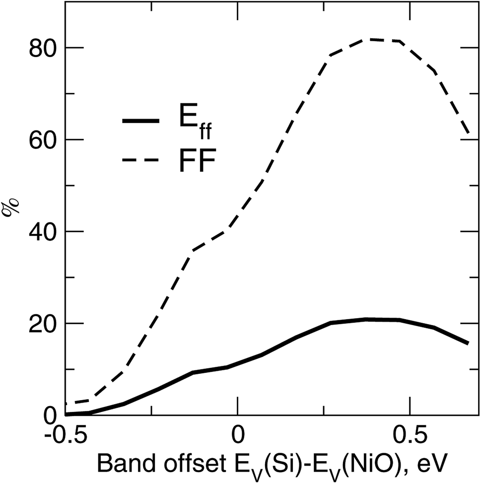 | ||
| Fig. 6 Conversion efficiency Eff and fill factor FF versus the band offset between c-Si and the oxide EV(Si)–EV(NiO), as determined from the TCAD simulations20 of the PV cell. | ||
The actual derivation of the electronic structure at the interface is quite demanding as it requires the large-scale computations. Here, an attempt is made to test the widely accepted affinity rule used for aligning the bands at heterojunctions, thus determining the band alignment within two approaches – the computationally less demanding case of isolated constituent layers and the case of a slab approach which involves all the component layers. The latter can be assessed straight from the partial density of states (DOS), as illustrated in Fig. 8, where Si-projected valence states are singled out from the total DOS. As shown, there are two situations considered here, – Ni-rich interface (NRI) between c-Si and the oxide, with its structure illustrated in Fig. 7, and O-rich interface (ORI), with its structure depicted earlier in Fig. 5.
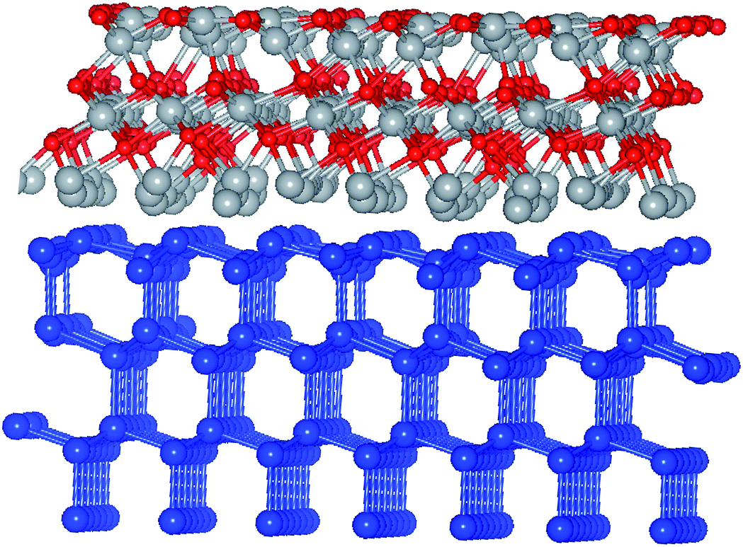 | ||
| Fig. 7 Ball and stick model of relaxed/NiO/Ni/c-Si(111), Ni-rich interface. Small red balls stand for O, blue balls are for Si, gray balls are for Ni. | ||
The main distinction is due to the different alignment of the valence states: in the case of NRI, the valence states of Si and NiO are aligned at around 0 eV, whereas there is an offset of roughly 0.4 eV between valence state edges in the case of ORI. The results are somewhat expected, considering the fact that Ni and Si atoms have a similar electronegativity. Alternatively, effects of the interface charge transfer effects21 can also be revealed by analyzing the average electrostatic potentials plotted for the entire slab in Fig. 8, two bottom panels, for both cases of Ni-rich and O-rich interface between Si and Ni oxide, respectively.
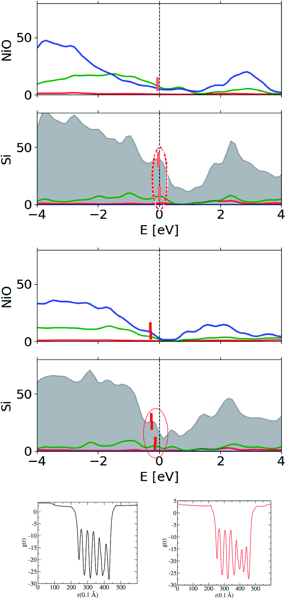 | ||
| Fig. 8 DOS of NixOy/c-Si(111), total (gray) and Si-site resolved, and the average electrostatic potential through the slab. Ni-rich interface is shown in the topmost, whereas O-rich interface between c-Si and nickel oxide is depicted in the panel below. Red, green and blue lines stand for the partial s-, p-, and d-orbital DOS. Positions of the valence state edges are marked with vertical red bars and outlined with an ellipse. Two bottom panels are for the potentials of Ni-rich and O-rich slabs, respectively. | ||
Since the vacuum levels are well aligned in all situations and thus the effect of the dipole field is moderated, there is a good chance the valence states are being aligned self-consistently in accord with the “mid-gap” energy EB,21 which separates valence band states from conduction states in the gap. Summarizing, the slab simulations reveal a dipole layer associated with the interface between c-Si and the AlNiO oxide, which electrostatically introduces a band offset detrimental to the charge selectivity. Thus, the affinity rule needs to be modified accordingly. A locally variable stoichiometry design implying Ni-rich junction is suggested as a countermeasure to eliminate the polarization field and achieve a band lineup suitable for hole transport and efficiency as high as 21%.
3 Photoionization studies: theoretical multiple-scattering approach including self-energy-induced state gap
A theoretical evaluation of the photo-induced current is done within a so-called one-step angular resolved PE method, based on the multiple scattering of the photo-excited carriers (see ref. 10 and references therein). The method delivers the layer and quasi-momentum k∥ resolved density of states, which are obtained using the relativistic multiple-scattering formalism based on the Green function approach. It uses the self-consistent atomic potentials generated by Linear Muffin-Tin Orbitals (LMTO) method after the atoms are structurally relaxed within the VASP-PAW method as described above. A separate treatment of the photoexcited electron and hole dynamics inside the truncated solid is achieved in terms of their self-energy using the atomic potentials within the multiple-scattering formalism and the technique of the Dyson equations for the retarded layer Green function. The life-time effects are accounted for by the imaginary part of the self-energy (∑). For the upper states, ∑ has been set to −2 eV, as suggested by low-energy electron diffraction (LEED) experience (cf. ref. 22, chapter 4). For occupied states, an energy-dependent function ∑ = ∑occ(1 − E/EF)α was used in the evaluation of the photoemission spectra, which however needs to be adjusted to the measured data and is therefore a quantity best determined a posteriori. Currently, a linear dependence with α = 1 was used, which has been shown to be a reasonable approximation in general (cf. e.g. ref. 23). The real part of the self-energy is uniform for both hole and electron states, i.e., no corrections to the Kohn–Sham eigen-states have been considered. As a consequence, the gap-associated problems persist. The electrostatic effect due to the surface image potential is modeled by a barrier in the form of step function positioned at 1/3 of the lattice parameter above the surface, which position otherwise needs to be re-adjusted a posteriori if there is a well defined outstanding surface state. No such state could be identified so far, although the surface effects are definitely the main focus of the present PE investigation.In the derivation of the layer and k∥-resolved density of states, the self-energy was set to a uniform 0.1 eV for all states to keep states equally distinguishable at all energies to ease the analysis. However, a larger value of 0.3 eV for the imaginary part of the self-energy of the occupied states was used in order to match the rather broader features of the measured PE spectra. No further refinement of the self-energy dependence on the state energy was pursued at this point in order to keep the interpretation as feasible as possible.
To address the usual problem of the Local Density Approximation (LDA)-caused flaw leading to an under-estimated energy gap, the state-dependent local self-energy was designed such that the states around the Fermi level are over-damped within a range of the predefined energies. Currently, Im∑(E) is approximated as
| Im∑(E) = Im∑0(1 + ξ2N)−1 + Im∑1, | (1) |
 The expression given by eqn (1) is in the form of maximally flat binomial suggested to serve as a band stop within the gap energy range G around the Fermi level EF. The flatness is determined by the power N = 1, 2,… – the higher the power the sharper the walls of the band stop range. Currently, Im∑0 is set to −10 eV within the gap, N = 1, and G = 3.6 eV in order to secure 3.6 eV of the gap size at the half-width of Im∑(E) maximum. In the context of the photoemission simulations, this gap-inducing self energy approach will be coined as GSE. Outside the gap, the slow E-dependent part Im∑1(E) is set to − 0.3 eV for occupied states in order to facilitate the comparative analysis. No temperature dependence is assumed for the same reason. In other words, the state E life time τ(E) = ℏIm∑(E)−1 vanishes within the gap and restores to ℏIm∑1(E) outside the gap.
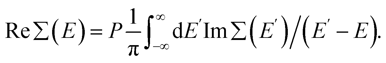
The expression for Im∑(E) in eqn (1) is slightly different from the one used before.9 It allows an easy analytical Kramers–Kronig transformation using the residue theorem in order to retrieve Re∑(E):
 | (2) |
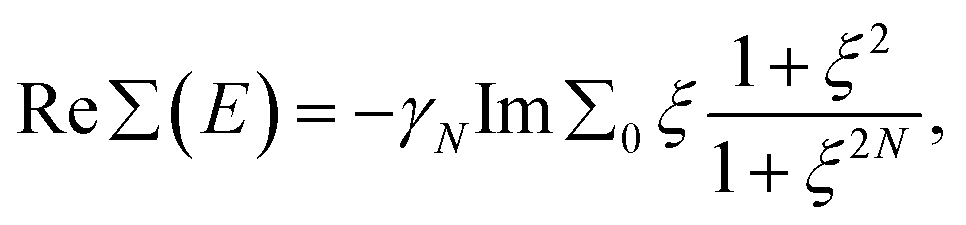
Thus, within the gap range, Re∑(E) has a closed form written for N = 1, 2 as
 | (3) |
 for γ1, γ2, respectively. As a reminder, the vacuum level is assumed as the energy reference in all layer Green function (LGF) approach expressions. The sketch of the self-energy in the LGF approach to simulate the effect of the state overdamping for PE simulations in the region of the insulating gap is depicted in Fig. 9. It has an expected energy dependence with Re∑(E) redistributing the state energies around the gap, pushing those away from the mid-gap toward the gap edges. The spatially uniform and state-dependent self-energy serves as a non-hermitian part in the effective single-quasi-particle Dyson equation
 | (4) |
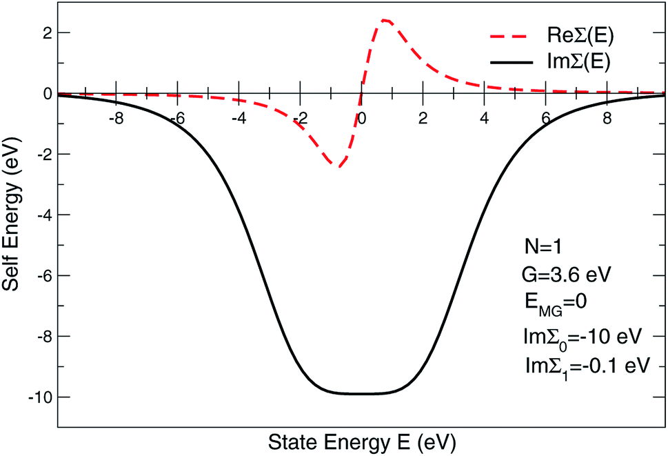 | ||
| Fig. 9 Self-energy sketch as used in layer multiple scattering method to simulate the effect of the state overdamping while PE simulations in the region of the electron band gap. | ||
4 ARPES analysis of NiO (001)
The approach of LDA combined with the GSE method, modelled in accord with eqn (2), is implemented here in order to simulate the layer-resolved density of states and most importantly the photo-current. The Im∑ is set to a relatively small value of 0.1 eV to emphasize the details of the electronic structure, which actual magnitude of about 0.3 eV was established from the PE data for the occupied states. As shown on Fig. 10, the crystalline-phase measured24 and calculated PE spectra are in a modest agreement in the range of binding energies up to 5 eV, which is heavily dominated by 3d states of Ni both on the surface and in the bulk. As mentioned above, the lifetime of the valence state carriers in the crystalline sample is estimated at τ ∼ ℏ/0.3 eV ∼ 0.310−14 s. On the other hand, our ALD-grown film measured PE spectra hints toward τ ∼ 10−15 s for the hole lifetime, as the intensity maxima are much broader. The reason a broadening of a PE curve is considered as contributed mostly by hole states is due to the fact the quasi-particles group velocities along the stacking direction v⊥ are much smaller that those for final states due to relatively narrow occupied d- and p-states for binding energies at around 2 eV.25 The range of binding energies higher than 5 eV, contributed mostly by 2p O states, is challenging for a comparative analysis as no subtraction of the secondary electron emission in the measurements is performed. However, since the ordinary single-particle Kohn–Sham band description doesn't really apply to a strongly-correlated system such as NiO,26 even after taking into account the electron–hole interaction using e.g. GW approximation,27,28 no derivation of the band dispersion is currently pursued. Instead, the focus here is on the trends related to the effects of the alloying, and the more appropriate Mott–Hubbard picture involving the charge fluctuations is replaced here a posteriori with the GSE method to capture the essential physics of both the excited and the ground states.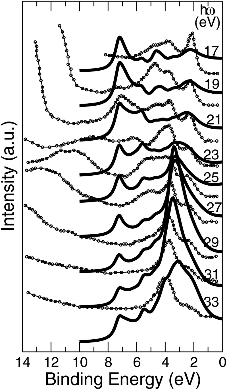 | ||
| Fig. 10 Normal emission data from the NiO (001) surface, k∥ = 0. Theory is plotted using bold lines. Experimental data24 shown in circles are for crystalline sample. | ||
5 ARPES analysis of Ni1−xAlxO (001)
The UV PE spectra of Al0.5Ni0.5O compound are in striking contrast to the one of NiO, as is easily seen in Fig. 11. Due to presence of trivalent Al, the electronic levels of O atoms are more exposed to the field of the nucleus and as a result are shifted to higher binding energies. The PE spectra are now are considerably wider and extend beyond 10 eV of the binding energies versus 8 eV only in NiO.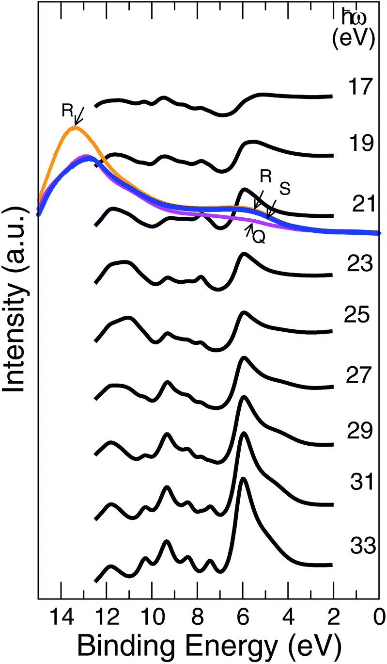 | ||
| Fig. 11 Normal emission simulated data from the Al0.5Ni0.5O (001) surface, k∥ = 0, bold black lines. The shown are also data measured at 21.0 eV of the photon energy for samples Q, R, S, as described in the text. | ||
The measured UV PE spectral data shown in Fig. 11, are recorded for 21.5 eV incident photons produced by the helium-I source lamp from samples Q, R and S. As mentioned above, the valence states are broader by about 2 eV and extend to higher binding energies up to 11 eV if Ni partially substituted by Al. The distinctions between the simulated photocurrent spectra of Al0.50Ni0.50O and NiO are easy to track by looking at Fig. 12, where the emission intensity magnitudes are normalized per same area and unit cell and computed for the same photon energy of 21 eV. Substituting Ni with Al leads to a reduced photoemission between 2 eV and 6 eV and makes the O contribution spread over wider range of the binding energies between 4 and 11 eV. To match the measured PE spectra, by an order of magnitude higher self-energy Im∑ = −0.5 × (1 − E/EF) is used in case of Al alloy, as opposed to the case of NiO. Thus derived self-energy for occupied states can serve as indirect evidence of the hole lifetime being by an order of magnitude smaller in Al alloys than in NiO, obviously related to the quality of the atomic ordering. The TEM of all samples also confirms essentially higher degree of the structural ordering in pure NiO than in the Al alloys. Therefore, in the context of a potential transport layer in a solar cell, the expected mobility of the hole carriers in Al alloys is by an order of magnitude lower than in NiO lightly-dopped with Al, which might impact the reverse saturation current and deteriorate the open-circuit voltage of the cell. However, even in its present realization, a simple annealing at 300 °C of the Al alloy is shown to have lower contact resistivity of 41.6 mΩ cm2 than that of NiO.
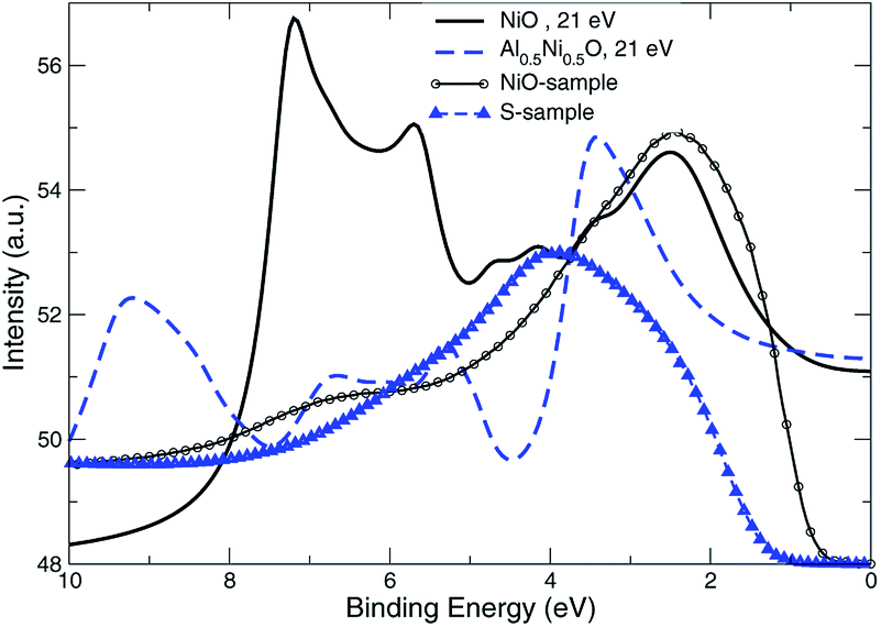 | ||
| Fig. 12 Normal PE data for NiO and Al0.5Ni0.5O, theory is plotted with bold and dashed lines. The shown are also data measured at ℏω = 21.0 eV: line with circles for NiO, and line with triangles for S-sample. | ||
The fact that there is a good chance to have a disordered combination of Al2O3 and NiO rather than substitutional alloy with limited ordering assumed in simulations, is anticipated given the ALD method currently used for the film fabrication. Moreover, pure Al2O3 has no discernible features between 2 and 6 eV.29,30 This observation indicates the presence of Ni3+ ions in the Al alloy structure, which content grows as the concentration of Al goes up. That the ratio Ni3+/Ni2+ for concentration strongly depends on the Al content, was also confirmed by our XPS Ni 2p3/2 measurements.
6 Summary
NiO alloyed with aluminum, Ni1−xAlxO, was analyzed in terms of its stoichiometry, electronic and transport properties, as well as interfacial band alignment with Si considering its potential use as a transport layer in p–i–n type solar cells. The analysis was based on the component material and slab structural simulations, as well as simulated and measured UV PES data, in order to reveal the best suitable stoichiometry. It is concluded that the ionization energy from the highest occupied states tends to grow with Al content as the simulated work function grows from 4.1 eV in pure NiO to 4.7 eV in heavily alloyed Al0.50Ni0.50O. The affinity rule is tested by evaluating the workfunctions of the component layers and justified best for a particular interface design – by adding Ni-enriching step to the oxidation cycle. Contrasting the simulated and measured UPS data allows the estimating the self-energy of the hole carriers, which in case of non-annealed Al-rich samples is shown to be by an order of magnitude higher due to the effects of disorder. The work functions derived from the measured UPS data for the ALD grown oxide films with nearly the same alloy stoichiometry correlate well with the simulated values. The findings suggest Ni coating of the back of silicon first, followed by a graded doping AlxNi1−xO, with high Al content at contact/oxide interface and low content at oxide/semiconductor, as the best design for HTL.Conflicts of interest
There are no conflicts to declare.Acknowledgements
The project is funded by Qatar National Research Fund (QNRF) through the National Priorities Research Program grants (NPRP9-021-009, NPRP X-107-027). Computational resources were provided by the research computing group at Texas A&M University in Qatar.References
- X. Yang, J. Guo, Y. Zhang, W. Liu and Y. Sun, J. Alloys Compd., 2018, 747, 563 CrossRef CAS.
- J. Lee, Y. Wook, N. Su, J. Sang, H. Jae and W. Jung, J. Power Sources, 2019, 412, 425 CrossRef CAS.
- M. Gong, W. Zhou, M. Tsai, J. Zhou, M. Guan, M.-C. Lin, B. Zhang, Y. Hu, D.-Y. Wang, J. Yang, S. J. Pennycook, B. Hwang and H. Dai, Nat. Commun., 2014, 5, 4695 CrossRef CAS PubMed.
- T. Zhang, M. Hossain, C.-Y. Lee, Y. Zakaria, A. Abdallah and B. Hoex, Appl. Phys. Lett., 2018, 113, 262102 CrossRef.
- J. Melskens, B. W. H. van de Loo, B. Macco, L. E. Black, S. Smit and W. M. M. Kessels, IEEE J. Photovoltaics, 2018, 8, 373–388 Search PubMed.
- M. B. Islam, M. Yanagida, Y. Shirai, Y. Nabetani and K. Miyano, ACS Omega, 2017, 2, 2291–2299 CrossRef CAS PubMed.
- S. Pang, C. Zhang, H. Dong, D. Chen, W. Zhu, H. Xi, J. Chang, Z. Lin, J. Zhang and Y. Hao, ACS Appl. Energy Mater., 2019, 2, 4700–4707 CrossRef CAS.
- A. M. Crowley and S. M. Sze, J. Appl. Physiol., 1965, 36, 3212 CrossRef.
- S. Halilov, E. Gorelov, M. Izquierdo, A. Yaroslavtsev, V. Aristov, P. Moras, P. M. Sheverdyaeva, S. K. Mahatha, F. Roth, A. Lichtenstein and S. L. Molodtsov, Phys. Rev. B, 2017, 96, 205144 CrossRef.
- S. Halilov, E. Tamura, D. Meinert, H. Gollisch and R. Feder, J. Phys.: Condens. Matter, 1993, 5, 3859 CrossRef CAS.
- S. M. Sze and K. K. Ng, Physics of Semiconductor Devices, Wiley and Sons, 2007 Search PubMed.
- M. D. Irwin, D. B. Buchholz, A. W. Hains, R. P. H. Chang and T. J. Marks, Proc. Natl. Acad. Sci. U.S.A., 2008, 105, 2783–2787 CrossRef CAS.
- G. Kresse and J. Furthmüller, Comput. Mater. Sci., 1996, 6, 15 CrossRef CAS.
- F. Lin, D. Nordlund, T.-C. Weng, R. G. Moore, D. Gillaspie, A. Dillon, R. Richards and C. Engtrakul, ACS Appl. Mater. Interfaces, 2013, 5, 301–309 CrossRef CAS PubMed.
- C. Flynn, S. McCullough, E. Oh, L. Li, C. C. Mercado, B. Farnum, W. Li, C. Donley, W. You, A. Nozik, J. McBride, T. Meyer, Y. Kanai and J. Cahoon, ACS Appl. Mater. Interfaces, 2016, 8, 4754–4761 CrossRef CAS PubMed.
- A. García-Escorial, P. Crespo, A. Hernando, M. Lieblich, P. Marín, V. Velasco and F. Ynduráin, J. Alloys Compd., 2014, 615, S645–S647 CrossRef.
- R. Martin, in Band Structure Engineering in Semiconductor Microstructures, Plenum, New York, NY, USA, 1989, vol. 189 Search PubMed.
- A. Franciosi and C. V. de Walle, Surf. Sci. Rep., 1996, 25, 1 CrossRef CAS.
- S. Halilov, A. A. B. Baloch, N. Tabet, S. N. Rashkeev and F. Alharbi, IEEE J. Photovoltaics, 2020, 10, 458 Search PubMed.
- Atlas User's Manual, Silvaco Inc, 2018 Search PubMed.
- J. Tersoff, Phys. Rev. B: Condens. Matter Mater. Phys., 1984, 30, 218 CrossRef.
- R. Feder, Polarised Electrons in Surface Physics, World Scientific, Singapore, 1985 Search PubMed.
- F. Aryasetiawan and O. Gunnarsson, Phys. Rev. Lett., 1995, 74, 3221 CrossRef CAS PubMed.
- Z.-X. Shen, C. K. Shih, O. Jepsen, W. E. Spicer, I. Lindau and J. W. Allen, Phys. Rev. Lett., 1990, 64, 2442 CrossRef CAS PubMed.
- N. V. Smith, P. Thiry and Y. Petroff, Phys. Rev. B: Condens. Matter Mater. Phys., 1993, 47, 15476 CrossRef CAS PubMed.
- S. Hüefner, Adv. Phys., 1994, 43, 183–356 CrossRef.
- S. V. Faleev, M. van Schilfgaarde and T. Kotani, Phys. Rev. Lett., 2004, 93, 126406 CrossRef PubMed.
- H. Jiang, R. Gomez-Abal, P. Rinke and M. Scheffler, Phys. Rev. B: Condens. Matter Mater. Phys., 2010, 82, 045108 CrossRef.
- J. Guo, D. E. Ellis and D. J. Lam, Phys. Rev. B: Condens. Matter Mater. Phys., 1992, 45, 13647 CrossRef CAS PubMed.
- W. J. Gignac, R. S. Williams and S. P. Kowalczyk, Phys. Rev. B: Condens. Matter Mater. Phys., 1985, 32, 1237 CrossRef CAS PubMed.
Footnote |
| † Designed Material Technologies, LLC, P.O. Box 14548, Richmond, VA 23221-9998, USA. |
| This journal is © The Royal Society of Chemistry 2020 |