
 Open Access Article
 This Open Access Article is licensed under a Creative Commons Attribution-Non Commercial 3.0 Unported Licence
Interfacial synthesis of a large-area coordination polymer membrane for rewritable nonvolatile memory devices†
Zepu Zhang‡
,
Yijie Nie‡,
Weiwei Hua,
Jingxuan Xu,
Chaoyi Ban,
Fei Xiu * and
Juqing Liu*
* and
Juqing Liu*
Key Laboratory of Flexible Electronics (KLOFE), Institute of Advanced Materials (IAM), Nanjing Tech University (NanjingTech), 30 South Puzhu Road, Nanjing 211816, China. E-mail: iamfxiu@njtech.edu.cn; iamjqliu@njtech.edu.cn
First published on 2nd June 2020
Abstract
The facile synthesis of large-area coordination polymer membranes with controlled nanoscale thicknesses is critical towards their applications in information storage electronics. Here, we have reported a facile and substrate-independent interfacial synthesis method for preparing a large-area two-dimensional (2D) coordination polymer membrane at the air–liquid interface. The prepared high-quality 2D membrane could be transferred onto an indium tin oxide (ITO) substrate to construct a nonvolatile memory device, which showed reversible switching with a high ON/OFF current ratio of 103, good stability and a long retention time. Our discovery of resistive switching with nonvolatile bistability based on the substrate-independent growth of the 2D coordination polymer membrane holds significant promise for the development of solution-processable nonvolatile memory devices with a miniaturized device size.
The exponential growth of communication for information and the miniaturization of electronic devices have caused an urgent demand for the design and preparation of new memory materials and devices.1–4 Organic/polymer memory devices have attracted considerable attention as promising alternatives to the conventional inorganic semiconductor-based memory devices.5 They have distinguished themselves as potential candidates for flexible and high-density data storage due to their low cost, structural tenability, mechanical strength, flexibility, and ease of processing.6–16 Nonetheless, the intrinsically weak intermolecular interactions between organic molecules result in low thermal stability and poor long-term environmental stability, which hinder their potential applications.17–19
As an important class of organic materials, coordination polymers demonstrate attractive switching properties and exhibit promising applications in the data storage field.20–22 Compared with polymers that have pure organic skeletons, coordination polymers comprising metal and organic ligands offer a potential alternative due to their facile preparation and high thermal stability, combining the advantages of both polymers and metal complexes. Particularly, by the flexible design of metal and organic constituents as well as by modifying the functional groups in the coordination complexes, the properties of memory devices based on the resultant coordination polymers can be fine-tuned.15 For instance, ternary resistive random access memory devices have been fabricated from one-dimensional conjugated coordination polymer chains coordinated with Co ions,23 which exhibit excellent thermal and long-term stability benefiting from their strong intermolecular interactions. Moreover, the successful growth of high-quality metal–organic framework (MOF) membranes on flexible gold-coated polyethylene terephthalate (PET) substrates has been achieved by liquid phase epitaxy for practical wearable information storage applications; moreover, a uniform and reproducible resistive switching effect has been observed.24
Besides molecular design, the formation of the thin films of active materials is crucial for the memory performance and coordination polymers downsized to nanoscale membranes with controllable electrical conductivity are promising for high-density data storage with a miniaturized device size. To date, vacuum-deposited, spin-coated or inkjet-printed films of the as-synthesized memory materials have been reported for memory applications.25 Unfortunately, severe problems such as easy cracking, unsatisfactory uniformity and thickness uncontrollability usually accompany the above-mentioned elaborate membrane deposition approaches, seriously limiting the memory performance. To address these issues, the growth and preparation of high-quality memory material membranes through facile chemical synthesis has been an urgent demand. Currently, liquid phase epitaxy or a layer-by-layer (LbL) approach is commonly used to grow high-quality coordination polymer membranes on organically functionalized surfaces for memory devices.26 Memory devices based on LbL approach-processed coordination polymer membranes have been reported to show excellent switching performance with a high ON/OFF current ratio and multilevel storage. Though the LbL approach offers unique opportunities, the substrate-dependent characteristics of the LbL thin-film preparation scheme seriously limit the applications of coordination polymers in memory devices. Despite the above-mentioned advances, coordination polymer membranes with an appropriate molecular design concomitant with a good film preparation approach are still urgently needed to obtain high-performance memory devices.
In this work, we have presented a facile and substrate-independent interfacial synthesis method for the preparation of a continuous and large-area coordination polymer membrane with nanoscale thickness at the air–liquid interface. The high-quality two-dimensional (2D) membrane can be transferred onto an indium tin oxide (ITO) substrate as the active layer to construct a nonvolatile memory device. The sandwiched device shows excellent rewritable nonvolatile memory performance with a low operational voltage, a large ON/OFF ratio, good stability and a long retention time.
Through a mild coordination reaction between a cobalt salt and the ligand 1,2,4,5-benzenetetramine tetrahydrochloride, a large-scale d–π conjugated coordination polymer membrane at the air–liquid interface can be prepared (Fig. 1). The resulting brown membrane demonstrates great substrate independence and can be transferred on to any substrate by dipping the support in the reaction solution and then lifting the membrane, making it practically applicable in diverse fields. The scanning electron microscopy (SEM) characterizations of the as-prepared membrane transferred onto the SiO2/Si substrate indicated a large-scale and continuous distribution of the membrane with a uniform thickness of ∼300 nm.
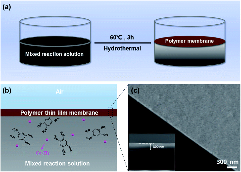 | ||
| Fig. 1 (a) Illustration of the polymer membrane formation process at the interface. (b) Schematic of the polymer membrane at the air–liquid interface. (c) SEM images of the as-prepared membrane with a thickness of 300 nm. | ||
The structure of the as-prepared brown membrane was characterized by powder X-ray diffraction (PXRD) utilizing two individual scattering geometries, namely, out-of-plane scattering geometry and in-plane geometry. The PXRD profile obtained using grazing-incidence XRD is presented in Fig. 2a. Different diffraction patterns were observed under these two XRD scattering geometries, suggesting an orientation-dependent characteristic of the prepared membrane (Fig. 2b).27 X-ray photoelectron spectroscopy (XPS) of the as-prepared membrane was conducted (Fig. 2c and S1†). The strong peak at 399.1 eV suggests a strong coordination between Co(II) and the ligand. The quantification of the elements present in the coordination polymer membrane based on XPS analysis demonstrated a 3.53![[thin space (1/6-em)]](https://www.rsc.org/images/entities/char_2009.gif) :1 atomic ratio of N:Co (Table S1†), which was close to the theoretical stoichiometric ratio (4:1) for the membrane structure, as shown in the inset of Fig. 2d; this further confirmed the strong coordination between one Co cation and two benzenetetramine groups of the organic ligand.28 In addition, the characteristic N–H stretching mode of –NH2 disappeared in the IR spectra after the reaction,29 whereas the phenyl-related vibration remained, further indicating that the coordination reaction occurred (Fig. 2d). On the basis of facile preparation, substrate independence, highly oriented structure and d–π conjugation construction facilitating carrier transportation, the synthesized 2D coordination polymer membranes are expected to possess potential applications in electronic devices.
:1 atomic ratio of N:Co (Table S1†), which was close to the theoretical stoichiometric ratio (4:1) for the membrane structure, as shown in the inset of Fig. 2d; this further confirmed the strong coordination between one Co cation and two benzenetetramine groups of the organic ligand.28 In addition, the characteristic N–H stretching mode of –NH2 disappeared in the IR spectra after the reaction,29 whereas the phenyl-related vibration remained, further indicating that the coordination reaction occurred (Fig. 2d). On the basis of facile preparation, substrate independence, highly oriented structure and d–π conjugation construction facilitating carrier transportation, the synthesized 2D coordination polymer membranes are expected to possess potential applications in electronic devices.
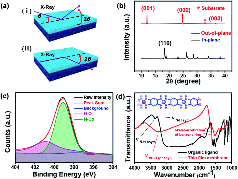 | ||
| Fig. 2 (a) The orientation of the films for (i) out-of-plane XRD scan and (ii) in-plane XRD scan. (b) PXRD profiles of out-of-plane XRD and in-plane XRD of the polymer membrane. (c) N 1s core level spectra of the membrane. (d) FT-IR spectra of the membrane and the ligand; the inset is the structure of the polymer membrane. | ||
With the use of the synthesized coordination polymer membrane as the active material layer, a typical memory device with the Al/polymer membrane/ITO sandwich structure was fabricated by directly transferring the as-prepared membrane with a thickness of 300 nm from the air–liquid interface onto the ITO substrate, followed by the thermal evaporation of the top Al electrodes (inset of Fig. 3a). The as-fabricated device exhibited progressively increasing injection currents as the initial voltage was swept from 0 to −5 V (ITO as the reference level, Sweep 1), and a sharp increase from 10−5 A to 10−2 A was observed at a switching threshold voltage of −1 V (Fig. 3c), indicating the device transition from a high-resistance state (OFF state) to a low-resistance state (ON state). This electrical transition from OFF to ON states represents the “writing” process of the memory device. Significantly, the abrupt increase in the current level with a high current ratio of 103 contributed to a minimal misreading error for the memory device and a small switching threshold voltage of −1 V was desirable for low-power memory applications. The device maintained the ON state with high stability in the subsequent voltage sweep (Sweep 2). When the voltage was swept from 0 to 5 V (Sweep 3), an abrupt decrease in the current was observed at the threshold voltage of about 3 V and the transition from the ON state to OFF state was equivalent to the “erasing” process. Furthermore, the device maintained the OFF state with high stability in the subsequent voltage sweep (Sweep 4). The current–voltage curve sweeps revealed an integrated write-read-erase-read switching process of this memory cell, suggesting a typical nonvolatile bistable FLASH-type memory device.
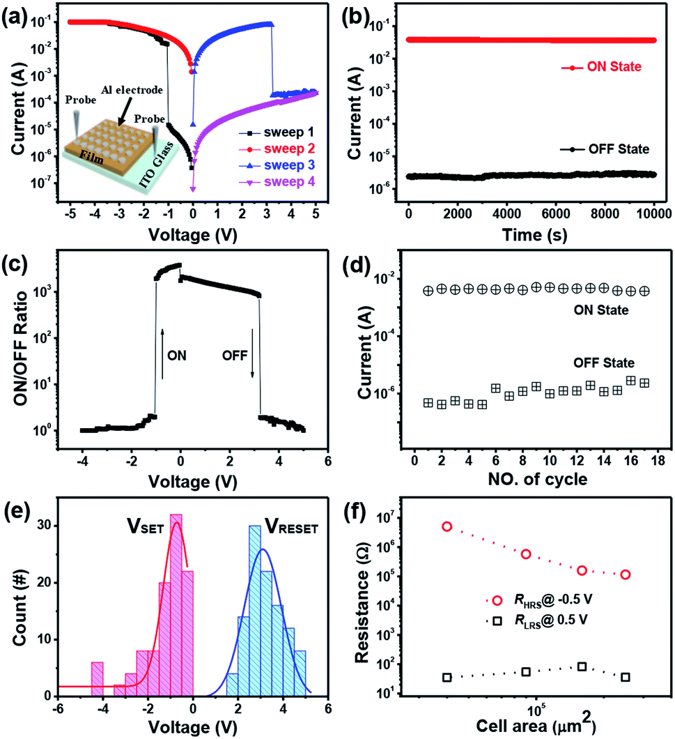 | ||
| Fig. 3 (a) I–V curves of the Al/polymer membrane/ITO memory device. Inset: schematic of the device structure. (b) Retention ability test of the device at a reading voltage of −0.5 V in the HRS and LRS states. (c) The ON/OFF ratio of the device under different applied voltages. (d) Currents of the device in the ON and OFF states. (e) Statistic histograms of SET/RESET voltages. (f) The cell area dependence of resistances in HRS and LRS. | ||
Moreover, the long-term stability of the coordination polymer memory device was evaluated from the retention time tests in both the ON and OFF states (Fig. 3b). Under a constant voltage stress of 0.5 V, the OFF state current remained stable but with some slight variations. When a bias of −0.5 V was applied, the device exhibited a stable current of about 0.04 A (ON state) for up to 10000 s and no significant decrease was observed. A high ON/OFF current ratio of 103 was maintained and the precise control of both ON and OFF states promised a quite low misreading rate of the memory device. To evaluate the reliability of memory devices, their cycling endurance was investigated. Fig. 3d shows that the OFF state currents remain between 4 × 10⁻⁷ and 3 × 10⁻⁶ A and the ON state currents range from 3 × 10⁻³ to 6 × 10⁻³ A. According to the statistical current distribution (measured at −0.5 V), no significant difference was observed in the ON/OFF state currents, indicating the good stability of the device. Compared with the endurance of previously reported devices,30,31 the endurance of our memory device is relatively short, which can be attributed to the fact that the top aluminum electrode is easily oxidized in an ambient environment without effective device packaging. It is expected that the device stability can be further improved if effective packaging is carried out or measurements are obtained in a vacuum system.
The uniformity in the distribution of switching voltages was evaluated by measuring 100 randomly selected device cells. Fig. 3e shows that the VSET values of most device cells are distributed in the range from 0 to −2 V and more than 50% devices exhibit a switching threshold voltage from 0 to −1 V. The average values of VSET and VRESET were −0.89 V and 3.09 V (the standard deviations were 0.26 (VSET) and 0.41(VRESET)), respectively, which coincided well with the measured results of the as-fabricated FLASH memory device. Notably, the difference between VSET and VRESET was large enough to ensure a low misreading rate and promise reliability when a readout was made.
Moreover, the dependence of the device resistance on the cell area was systematically studied based on a series of controlling tests to explore the underlying switching mechanism in the as-fabricated memory cell (Fig. 3f). When the applied voltage was in the range from 1 to −0.5 V, the memory cell was in a high resistance state (HRS) and the resistance (RHRS) was inversely proportional to the cell area due to the homogeneous current flowing through the memory cell.32 In contrast, for the low-resistance state (LRS) from 0 to 0.5 V, RLRS was independent of the cell area, suggesting that the LRS was dominated by the localized conducting path.
To investigate the resistance mechanism of the 2D coordination polymer membrane-based memory device, logI–logV plots were studied to analyze the carrier transport mechanism of the OFF and ON states (Fig. 4a and b). The fitting results reveal that the I–V curve of the flash memory device in the OFF state consists of two distinct linear regions, corresponding to the ohmic conduction mechanism and trap-limited space charge limited conduction (TL-SCLC) mechanism,33–39 whereas the device in the ON state only obeys the ohmic conduction mechanism. The corresponding resistive switching phenomenon was further studied by exploring the transportation mechanism of charge carriers via physical models (Fig. 4c–f). When a bias voltage was applied to the Al electrode and the scanning voltage was low, the density of the injected charge carriers was lower than that of the free carriers generated by thermal excitation in the film, which contributed to most of the charge transportation. The corresponding I–V curve shows linear behavior governed by ohmic conduction, resulting in a high resistance state (Fig. 4c). With the increase in the applied bias voltage, space charges appeared and some traps in the dielectric layer were occupied by the injected free carriers, leading to SCLC with limited trap filling dominating the carrier transport process, and the charge transport mechanism was dominated by TL-SCLC (Fig. 4d). With increasing carriers injected, the carrier transport changed from a trap-limited stage to a trap-free stage. When all the traps were filled, the injected carriers could move freely in the dielectric layer, which corresponded to trap-free SCLC conduction, indicating that the device underwent a transition from HRS to LRS. When the device changed to a low resistance state, the charge transfer still followed the ohmic conduction mechanism (Fig. 4f). The RESET process where the device changed from LRS to HRS (Fig. 4b) showed an I ∝ V relationship in the low resistance state, indicating that ohmic conduction dominated the charge transport process. As the device transfer to HRS, the trap center releases charges from a fully filled state to an unfilled state which shows a I ∝ V2 relationship. Then the state is continuously dominated by ohmic conduction. The device exhibited typical non-volatile flash characteristics, affording new ways to achieve 2D coordination polymer membrane-based memory devices via interfacial nanostructure engineering.
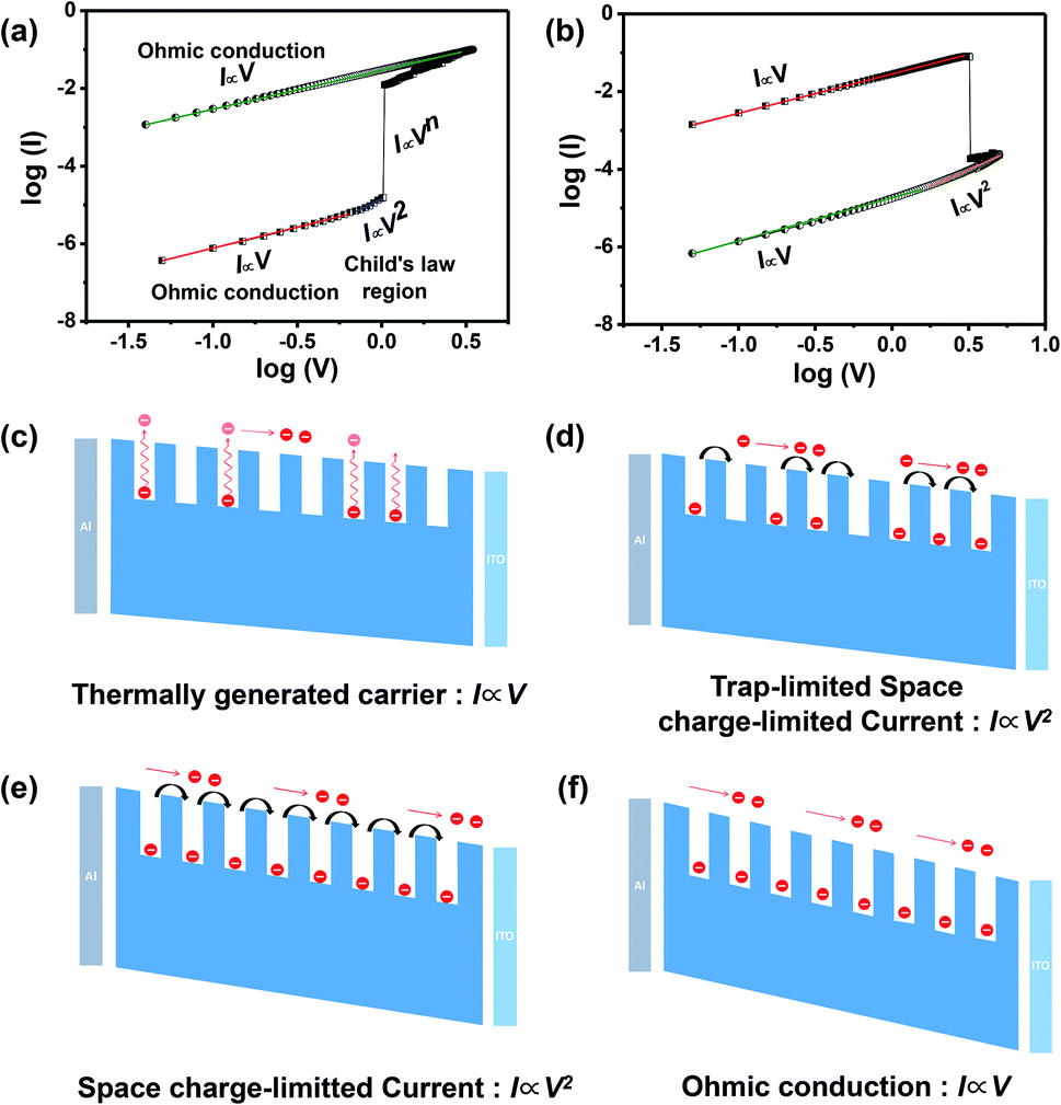 | ||
| Fig. 4 (a) Fitted I–V curves of the memory device at the SET process. (b) Fitted I–V curves of the memory device at the RESET process. (c–f) Transportation mechanisms of charge carriers from low conductive state to intermediate conductive state and further to high conductive state. | ||
Conclusions
In summary, we have successfully prepared a large-area and continuous 2D coordination polymer membrane by a facile interfacial synthesis method. Importantly, the as-prepared high-quality 2D membrane can be transferred onto any substrate, demonstrating great substrate independence. Moreover, a sandwich-structured memory device was fabricated with the prepared polymer membrane as the active material; the device exhibited excellent rewritable nonvolatile memory performance with a low operational voltage, high ON/OFF ratio and good stability, making coordination polymer membranes promising candidates for the development of solution-processable nonvolatile memory devices with a miniaturized device size.Conflicts of interest
There are no conflicts to declare.Acknowledgements
We thank primary financial supports by the National Key R&D Program of China (2017YFB1002900), the National Natural Science Foundation of China (61622402, 51703093, 61376088), the Natural Science Foundation of Jiangsu (BK20171000, BK20150955), the Jiangsu Specially-Appointed Professor Programme, the Six Talent Plan (2015XCL015).Notes and references
- J. Liu, F. Yang, L. Cao, B. Li, K. Yuan, S. Lei and W. Hu, Adv. Mater., 2019, 31(28), 1902264 CrossRef PubMed.
- E. C. Ahn, H. S. P. Wong and E. Pop, Nat. Rev. Mater., 2018, 3(3), 18009 CrossRef CAS.
- M. Wang, S. Cai, C. Pan, C. Wang, X. Lian, Y. Zhuo, K. Xu, T. Cao, X. Pan, B. Wang, S. J. Liang, J. J. Yang, P. Wang and F. Miao, Nat. Electron., 2018, 1(2), 130–136 CrossRef CAS.
- S. Goswami, A. J. Matula, S. P. Rath, S. Hedstrom, S. aha, M. Annamalai, D. Sengupta, A. Patra, S. Ghosh, H. Jani, S. Sarkar, M. R. Motapothula, C. A. Nijhuis, J. Martin, S. Goswami, V. S. Batista and T. Venkatesan, Nat. Mater., 2017, 16(12), 1216–1224 CrossRef CAS PubMed.
- H. C. Wu, A. D. Yu, W. Y. Lee, C. L. Liu and W. C. Chen, Chem. Commun., 2012, 48(73), 9135 RSC.
- S. J. Liu, P. Wang, Q. Zhao, H. Y. Yang, J. Wong, H. B. Sun, X. C. Dong, W. P. Lin and W. Huang, Adv. Mater., 2012, 24(21), 2901–2905 CrossRef CAS PubMed.
- M. Lyu, Y. Liu, Y. Zhi, C. Xiao, B. Gu, X. Hua, S. Fan, Y. Lin, W. Bai, W. Tong, Y. Zou, B. Pan, B. Ye and Y. Xie, J. Am. Chem. Soc., 2015, 137(47), 15043–15048 CrossRef CAS PubMed.
- H. C. Chang, C. L. Liu and W. C. Chen, Adv. Funct. Mater., 2013, 23(39), 4960–4968 CrossRef CAS.
- Q. Zhang, J. He, H. Zhuang, H. Li, N. Li, Q. Xu, D. Chen and J. Lu, Adv. Funct. Mater., 2016, 26(1), 146–154 CrossRef CAS.
- C. T. Poon, D. Wu, W. H. Lam and V. W. Yam, Angew. Chem., Int. Ed. Engl., 2015, 54(36), 10569–10573 CrossRef CAS PubMed.
- V. K. Au, D. Wu and V. W. Yam, J. Am. Chem. Soc., 2015, 137(14), 4654–4657 CrossRef CAS PubMed.
- C. Wang, J. Wang, P. Z. Li, J. Gao, S. Y. Tan, W. W. Xiong, B. Hu, P. S. Lee, Y. Zhao and Q. Zhang, Chem.–Asian J., 2014, 9(3), 779–783 CrossRef CAS PubMed.
- Y. Chen, G. Liu, C. Wang, W. Zhang, R.-W. Li and L. Wang, Mater. Horiz., 2014, 1(5), 489–506 RSC.
- H. J. Yen, C. Shan, L. Wang, P. Xu, M. Zhou and H. L. Wang, Polymers, 2017, 9(1), 9010025 Search PubMed.
- W. Lv, H. Liu, W. Wang, E. Yang, H. Zhen and Q. Ling, RSC Adv., 2017, 7(30), 18384–18391 RSC.
- Y.-G. Ko, S. G. Hahm, K. Murata, Y. Y. Kim, B. J. Ree, S. Song, T. Michinobu and M. Ree, Macromolecules, 2014, 47(23), 8154–8163 CrossRef CAS.
- J. F. Tian, J. M. Cai, C. Hui, C. D. Zhang, L. H. Bao, M. Gao, C. M. Shen and H. J. Gao, Appl. Phys. Lett., 2008, 93(12), 122105 CrossRef.
- B. Hu, X. Zhu, X. Chen, L. Pan, S. Peng, Y. Wu, J. Shang, G. Liu, Q. Yan and R. W. Li, J. Am. Chem. Soc., 2012, 134(42), 17408–17411 CrossRef CAS PubMed.
- Z. Liu, J. He, H. Li, Q. Xu, N. Li, D. Chen, L. Wang, X. Chen, K. Zhang and J. Lu, Adv. Electron. Mater., 2016, 2(5), 1500474 CrossRef.
- J. Xiao, Z. Yin, Y. Wu, J. Guo, Y. Cheng, H. Li, Y. Huang, Q. Zhang, J. Ma, F. Boey, H. Zhang and Q. Zhang, Small, 2011, 7(9), 1242–1246 CrossRef CAS PubMed.
- M. H. Aslam, U. Farooq, M. N. Awais, M. K. Bhatti and N. Shehzad, Arabian J. Sci. Eng., 2016, 41(8), 3035–3049 CrossRef CAS.
- X. F. Cheng, E. B. Shi, X. Hou, J. Shu, J. H. He, H. Li, Q. F. Xu, N. J. Li, D.-Y. Chen and J. M. Lu, Adv. Electron. Mater., 2017, 3(8), 1700107 CrossRef.
- X. F. Cheng, E. B. Shi, X. Hou, J. Shu, J. H. He, H. Li, Q. F. Xu, N. J. Li, D.-Y. Chen and J. M. Lu, Adv. Electron. Mater., 2017, 3(8), 1700107 CrossRef.
- L. Pan, Z. Ji, X. Yi, X. Zhu, X. Chen, J. Shang, G. Liu and R. W. Li, Adv. Funct. Mater., 2015, 25(18), 2677–2685 CrossRef CAS.
- P. Y. Gu, F. Zhou, J. Gao, G. Li, C. Wang, Q. F. Xu, Q. Zhang and J. M. Lu, J. Am. Chem. Soc., 2013, 135(38), 14086–14089 CrossRef CAS PubMed.
- S. Rana, R. Rajendra, B. Dhara, P. K. Jha and N. Ballav, Adv. Mater. Interfaces, 2016, 3(13), 1500738 CrossRef.
- K. Otsubo, T. Haraguchi, O. Sakata, A. Fujiwara and H. Kitagawa, J. Am. Chem. Soc., 2012, 134(23), 9605–9608 CrossRef CAS PubMed.
- K. X. Niu, B. P. Yang, J. F. Cui, J. T. Jin, X. G. Fu, Q. P. Zhao and J. Y. Zhang, J. Power Sources, 2013, 243, 65–71 CrossRef CAS.
- M. V. Reddy, S. M. Kang, S. Yoo, S. S. Woo and D. W. Kim, RSC Adv., 2019, 9, 9435–9442 RSC.
- J. Liu, F. X. Yang, L. L. Cao, B. L. Li, K. Yuan, S. B. Lei and W. P. Hu, Adv. Mater., 2019, 31, 1902264 CrossRef PubMed.
- Y. h. Yin, Z. Zhou, X. J. Wang, H. W. Mao, C. Y. Ban, Y. B. Chen, J. Q. Liu, Z. D. Liu and W. Huang, ACS Appl. Mater. Interfaces, 2020, 12(1), 1103–1109 CrossRef CAS PubMed.
- T. W. Kim, H. Choi, S. H. Oh, M. Jo, G. Wang, B. Cho, D. Y. Kim, H. Hwang and T. Lee, Nanotechnology, 2009, 20(2), 025201 CrossRef PubMed.
- H. Wang, B. Zhu, X. Ma, Y. Hao and X. Chen, Small, 2016, 12(20), 2715–2719 CrossRef CAS PubMed.
- C. Chen, F. Pan, Z. S. Wang, J. Yang and F. Zeng, J. Appl. Phys., 2012, 111(1), 013702 CrossRef.
- D. S. Shang, Q. Wang, L. D. Chen, R. Dong, X. M. Li and W. Q. Zhang, Phys. Rev. B: Condens. Matter Mater. Phys., 2006, 73(24), 245427 CrossRef.
- R. Dong, D. S. Lee, W. F. Xiang, S. J. Oh, D. J. Seong, S. H. Heo, H. J. Choi, M. J. Kwon, S. N. Seo, M. B. Pyun, M. Hasan and H. Hwang, Appl. Phys. Lett., 2007, 90(4), 042107 CrossRef.
- F. Pan, S. Gao, C. Chen, C. Song and F. Zeng, Mater. Sci. Eng., R, 2014, 83, 1–59 CrossRef.
- Q. Liu, W. H. Guan, S. B. Long, R. Jia and M. Liu, Appl. Phys. Lett., 2008, 92, 012117 CrossRef.
- M. A. Lampert and P. Mark, Phys. Bull., 1970, 21(12), 558 Search PubMed.
Footnotes |
| † Electronic supplementary information (ESI) available. See DOI: 10.1039/d0ra02933e |
| ‡ Z. P. Z. and Y. J. N. contributed equally to this work. |
| This journal is © The Royal Society of Chemistry 2020 |