
 Open Access Article
 This Open Access Article is licensed under a Creative Commons Attribution-Non Commercial 3.0 Unported Licence
Light-induced surface patterning of alumina†
Jaeho Choia,
Hong Suk Kang b,
Wonhee Joa and
Hee-Tak Kim*ac
b,
Wonhee Joa and
Hee-Tak Kim*ac
aDepartment of Chemical and Biomolecular Engineering, Korea Advanced Institute of Science and Technology (KAIST), Daejeon, 305-701, Republic of Korea. E-mail: heetak.kim@kaist.ac.kr
bInterface Materials and Chemical Engineering Research Center, Korea Research Institute of Chemical Technology, Daejeon 34114, Republic of Korea
cAdvanced Battery Center, KAIST Institute for the NanoCentury, Korea Advanced Institute of Science and Technology, Daejeon, 305-701, Republic of Korea
First published on 27th May 2020
Abstract
Micro/nano-patterned alumina surfaces are important in a variety fields such as chemical/biotechnology, surface science, and microelectro-mechanical systems. However, for patterning alumina surfaces, it still remains a challenge to have a lithographic tool that has large flexibility in design layouts, structural reconfigurability, and a simple fabrication process. In this work, a new alumina-patterning platform that uses a photo-reconfigurable azobenzene–alumina composite as an imprinting material is presented. Under far-field irradiation, the azobenzene–alumina anisotropically flows in the direction parallel to the light polarization. Accordingly, an arbitrarily designed azobenzene–alumina composite by imprinting can be deterministically reconfigured by light polarization and irradiation time. The photo-reconfigured azobenzene–alumina is then converted to pure alumina through calcination in an air atmosphere, which provides thin crack-free alumina patterns with a high structural fidelity. The novel combination of photo-reconfigurable azobenzene moieties and an alumina precursor for imprinting the material provides large flexibility in designing and controlling geometric parameters of the alumina pattern, which potentially offers significant value in various micro/nanotechnology fields.
Introduction
Micro/nano alumina surface patterns are of great interest in a wide variety of fields such as chemical/biotechnology, surface science and microelectro-mechanical systems.1–8 This is mainly because the alumina possesses chemical endurance, mechanical stability, bio-inertness and biocompatibility.9 For example, a microgrooved surface of alumina was introduced to investigate cell activities such as adhesion, differentiation of osteoblasts and osteoblast-specific gene expression.10 In addition, alumina micro/nano patterns are intensively used as etch-masks to pattern functional materials such as silicon because alumina exhibits outstanding plasma-etch resistance.11–15One method to fabricate such alumina pattern is anodic aluminum oxide (AAO), which provides nanopore hexagonal arrays as oxidized aluminum self-organize during oxidation. This method is particularly interesting because it provides highly ordered nanopore hexagonal arrays with controlled aspect ratio at a low cost and deterministic control of diameter and space. However, the principle of pattern formation is based on intrinsic nature of self-organization, and the obtainable structure is mostly limited to hexagonal pore arrays, hindering flexible structural design.11 Photolithography can provide large flexibility in the design of micro/nano structural layouts of surface features.13,16,17 This method forms a pattern by selective exposure of light to photo-resist through photomask and transfer the pattern of photoresist to alumina. Therefore, any types of pattern can be obtained by properly designed photo-masks. However, the relatively complex process including align of photomask, exposure, development and etching is considered to hinder its general uses. In addition, it requires every other photo-masks for every other sizes or shapes of patterns due to the lack of reconfigurability of photomask, thus causing a high cost in structural optimization. Alternatively, much simpler fab-process of imprint lithography where it forms a pattern by molding or stamping alumina ink can be used, however, the pre-formed patterns still do not have structural reconfigurability.10
In this work, we develop a new platform for designing alumina surface patterns, which provides arbitrary design layouts and the control of geometries different from those of the original master patterns with a simple fab-process. The key to the success of our strategy is using polyazobenzene/alumina precursor blend (azo–alumina composite) as an imprinting material. Under far-field irradiation, the pre-patterned (imprinted) azo–alumina composite anisotropically flows in parallel to the polarization direction, and the degree of transformation can be precisely controlled by manipulating light polarization and irradiation time. Such structural reconfiguration originates from directional photofluidic behavior of azobenzene polymer, which attracts considerable intrigue to produce micro/nano-patterned surfaces.18–22 The photo-reconfigured azo–alumina composite patterns are then converted to pure alumina through calcination in air atmosphere, which provides crack-free thin alumina patterns with a high structural fidelity.
Experimental
Preparation of azo–alumina ink
The azo–alumina composite solution was prepared by mixing of an alumina precursor solution and an azopolymer solution. First, to prepare alumina precursor solution, we dissolved 4.06 mmol of aluminum-tri-sec-butoxide (97% assay, Sigma-Aldrich) in 3 g of NMP. To avoid the hydrolysis of aluminum-tri-sec-butoxide in air, the liquid aluminum tri-sec butoxide was quickly added to the NMP solvent. Then, 4.47 mmol of ethyl acetoacetate (≥97% assay, Sigma-Aldrich) diluted in 1 g of NMP was added to the solution to chelate the aluminum-tri-sec-butoxide. The excess supply of the chelating agent was intended to guarantee full chelation of the aluminum-tri-sec-butoxide.An azopolymer, polydisperse orange 3 (PDO3) with a molecular weight of 4700 g mol−1 and a polydispersity index of 1.74, was synthesized by reacting 5.8 mmol of bisphenol A diglycidyl ether (Sigma-Aldrich) and 5.8 mmol of disperse orange 3 (Sigma-Aldrich), as described elsewhere.23 Then, the 1 g of azopolymer was dissolved in 2 g of NMP and mixed with the chelated alumina precursor solution to obtain azo–alumina composite ink; the amount of azopolymer and alumina precursor solution was adjusted to have various alumina concentrations, while the total concentration of the azopolymer and alumina in the solutions was maintained at 14 wt%. For example, to prepare 17 wt% alumina-composition solution, 0.291 g of the alumina precursor and 1 g of the azopolymer solution was mixed, where 1.46 g of NMP solvent is added to adjust the total concentration at 14 wt%.
Preparation of mold
A PDMS mold containing a line array was replicated from a master silicon template. The silicon template prepared by conventional photolithography was treated with tridecafluoro-1,1,2,2-tetrahydrooctyl-1-trichlorosilane to change the surface hydrophobic. After the treat, a mixture of a PDMS elastomer base and a curing agent (Sylgard 184, Dow Corning, Midland, MI) at a weight ratio of 10![[thin space (1/6-em)]](https://www.rsc.org/images/entities/char_2009.gif) :1 was gently poured on the silicon template; the mixture was degassed by vacuum suction before use. After fully curing at 70 °C for 3 h, the PDMS mold was carefully released from the silicon master.
:1 was gently poured on the silicon template; the mixture was degassed by vacuum suction before use. After fully curing at 70 °C for 3 h, the PDMS mold was carefully released from the silicon master.
Molding of azo–alumina ink
A drop of the azo–alumina solution was deposited on a slide glass and the PDMS mold was gently placed over the drop; the slide glass was ultrasonically cleaned with acetone, ethanol, and deionized water in turn to remove surface contamination before use. The azo–alumina solution spontaneously filled the line-cavities of the PDMS mold by capillary force as illustrated in Fig. S1,† and the solvent was gradually evaporated as leaving the solid azo–alumina mixture behind. After full evaporation at 50 °C for 12 h, the PDMS mold was gently removed from the substrate, yielding the azo–alumina line pattern on the glass substrate.Optical setup for photo-reconfiguration
A 532 nm wavelength laser (diode pump solid-state, Melles Griot) with an output power of 20 mW was polarized using a set of half- and quarter-wave plates, which was then spatially filtered and collimated. The intensity of the beam was controlled by neutral density filters. The array of micro-lines was illuminated by the beam with a diameter of 1 cm for a controlled duration using an electronic shutter.Calcination of the azo–alumina pattern
The reconfigured azo–alumina array was calcined in an electric resistance furnace (home-built equipment) under atmospheric air. The sample was slowly heated to 100 °C at a constant ramp rate of 5 °C min−1 and held for 1 h. Then, the temperature was increased to 500 °C at the same ramp rate and kept for 3 h.Structural characterization
All of the structures developed in this study were characterized by SEM (FEI, Sirion) with field emission, AFM (psia XEI-100 systems) and FT-IR microscope (Bruker Optics, IFS66 V/S & HYPERION 3000). The AFM measurement was operated in noncontact mode under ambient conditions. The SEM samples were prepared by coating with 10 Å of platinum, and examined at 10 keV. Both plane and cross-sectioned views of the samples were examined using SEM.Results and discussion
The overall process for the photo-reconfigurable alumina patterning consists of three major steps as shown in Fig. 1a: (i) preparation of pristine azo–alumina pattern arrays on a substrate by solvent-assisted imprint lithography; (ii) structural reconfiguration of the arrays by photofluidization; and (iii) pyrolytic conversion of the reconfigured azo–alumina into an alumina.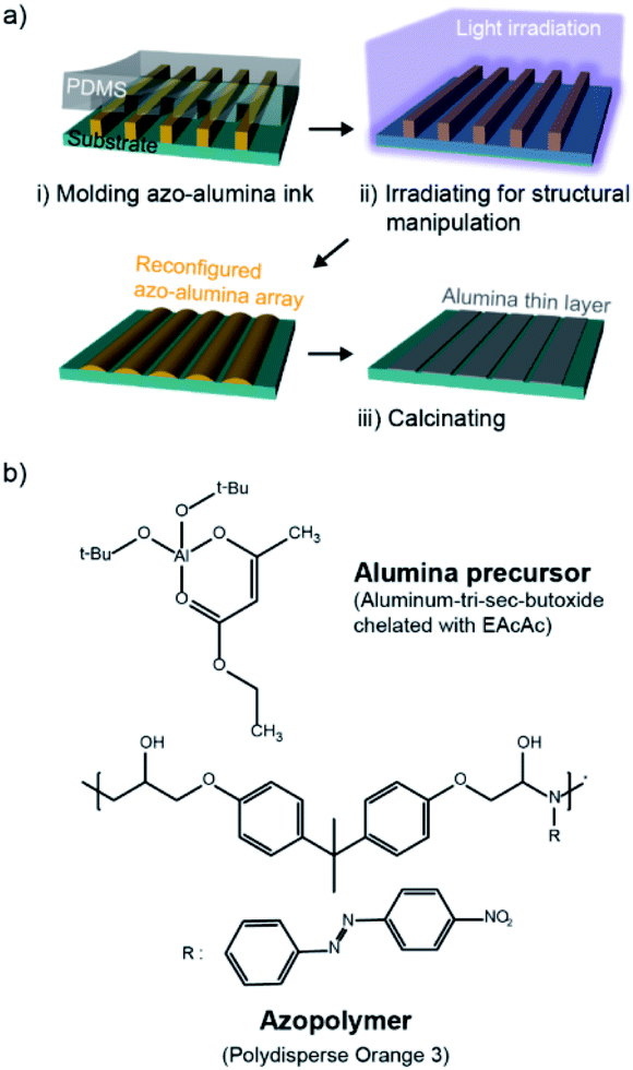 | ||
| Fig. 1 (a) The fabrication procedure of alumina patterns based on photo-reconfigurable azopolymer–alumina ink. (b) Chemical structures of the alumina precursor and azopolymer. | ||
The azo–alumina ink used for imprinting is a mixture of azobenzene polymer (azopolymer) and alumina precursor blended in NMP solvent (Fig. 1b). The azopolymer is polydisperse orange 3 (PDO3), an epoxy-based azobenzene molecule-containing amorphous polymer whose molecular weight is 4700 g mol−1. The alumina precursor is aluminum tri-sec butoxide that is chelated with ethyl acetoacetate (EAcAc). The chelation prevents the precipitation of the aluminum butoxide, ensuring a stable and homogenous mixture of the azopolymer and alumina precursor; ethyl acetoacetate is chosen for a chelating agent due to its high chelating ability for aluminum alkoxides.24,25
In addition, it should be noted that, unlike common sol–gel chemistry including a gelation of metal alkoxide through hydrolysis and condensation, our process thoroughly excludes the gelation of aluminum-butoxide. This is because an increased molecular weight by the gelation significantly reduces the speed of mass-migration during the reconfiguration process. The detailed procedure for preparing the azo–alumina ink is further described in Experimental section.
We choose micro-line array to demonstrate the structure reconfiguration. To prepare a pristine azo–alumina micro-line array, a drop of the azo–alumina ink was deposited on a freshly cleaned slide glass, then a PDMS mold containing line array was placed over the drop as illustrated in Fig. S1.† The azo–alumina ink spontaneously filled the line-cavities in the PDMS mold and the solvent gradually evaporated. As the solvent evaporated, the ink was spontaneously removed from the PDMS/substrate interface due to high surface energy of the ink, which forms a residual layer-free line array.26 Micro-molding method with the ink-filling from the open-end channel can also produce residue-free patterns, however, such strategies hinder fabricating dead end design structures.27 Therefore, to provide large flexibility in the design of micro/nano structural layouts of surface features, we exploited the solvent-assisted inprinting process as an original pattern-former. The resulting line array with a width, depth, and space of 1.5, 1.1, and 2.5 μm is shown in Fig. S2.† Note that such residual layer-free pattern array is advantageous for its use as etch-mask because the additional lithographic process to remove residue layer is not needed.
Directional photofluidization of azopolymer allows deterministic structural manipulation of the azo–alumina line array. For the manipulation, we controlled the line gap dimension by fluidizing azopolymer in a grating vector direction as schematically shown in Fig. 2a. To this end, a linearly polarized light parallel to the grating vector with a wavelength of 532 nm was irradiated. The irradiation induced the flow of the solid azo–alumina in the light polarization direction. Accordingly, the gap between the lines was gradually reduced as increasing the irradiation time. As shown in Fig. 2b, as increasing the alumina concentration from 0 to 33 wt%, both the speed of mass-migration and the moving distance were significantly reduced. This is because the concentration of the azobenzene moiety, which drives the mass-migration, is reduced as increasing the alumina concentration. For efficient mass-migration, we used azo–alumina with a 17 wt%-alumina concentration throughout this work. The SEM images of the reconfigured azo–alumina arrays with different irradiation time are shown in Fig. 2c. The gaps between the lines were 2.5, 1.0, and 0.5 μm at the irradiation time of 0, 5, and 10 min, respectively. Note that, based on this method, a wide range of structures can be fabricated by combining pre-pattern designs and light polarizations; examples include hole, pillar, and ellipsoidal arrays.28,29
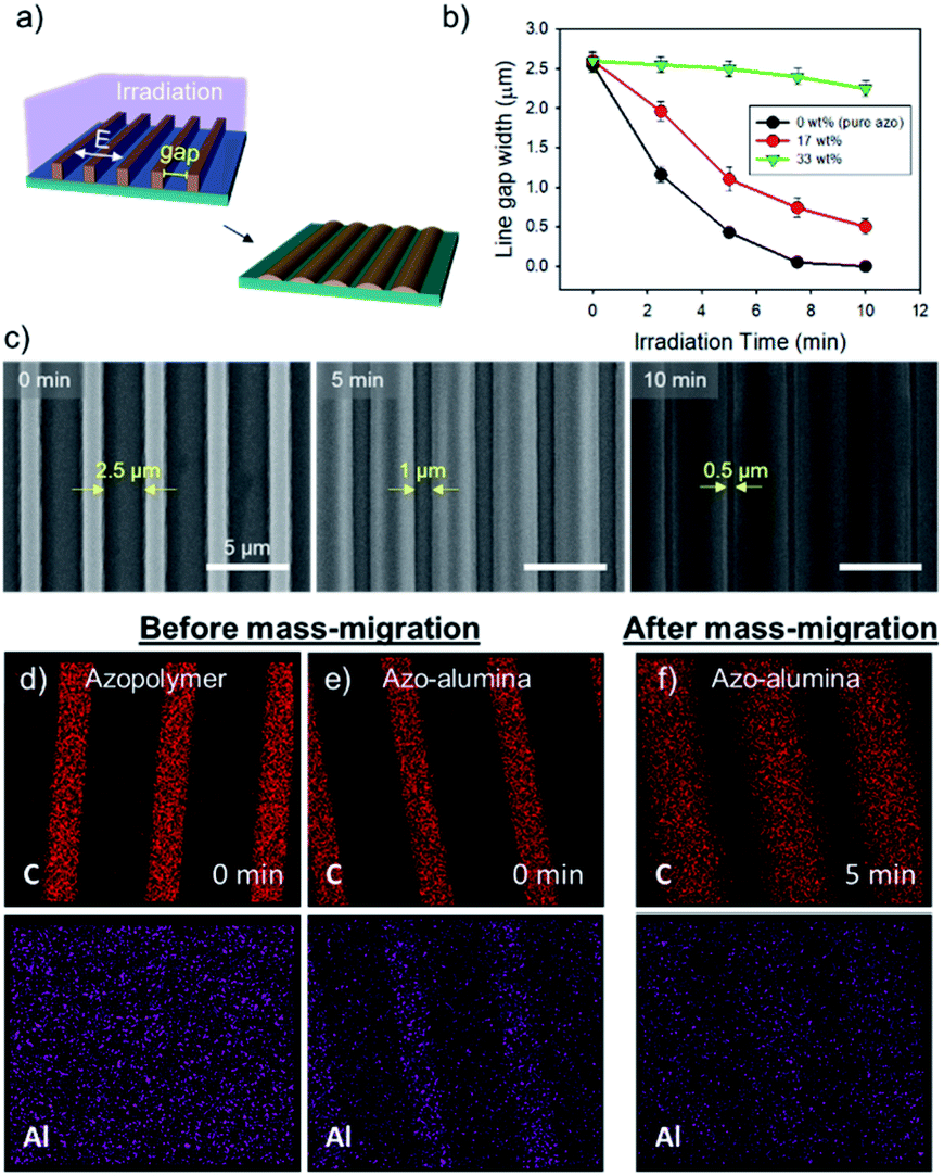 | ||
| Fig. 2 (a) Schematic diagrams of the structural reconfiguration of the azo–alumina line array: linearly polarized light perpendicular to the lines are irradiated to control the gap width. (b) The gap width as a function of irradiation time for three different alumina compositions of 0, 17, and 33 wt%; the error bars indicate the distribution of gap sizes measured by SEM at the irradiated area with a beam-diameter of 1 cm. (c) The scanning electron microscope (SEM) images showing the pristine and reconfigured line arrays (17 wt%) with the irradiation time of 5 and 10 min. (d) Elemental mapping (C and Al) of the azopolymer and azo–alumina composite (17 wt%) before and after mass-migration. | ||
To confirm the cooperative mass-migration of alumina and azopolymer, we tracked C and Al elements by EDX mapping. As shown in Fig. 2d and e, the as-fabricated azo–alumina line array exhibited C and Al elements along the lines, whereas, for pure azo-line array, such line configuration was absent for in the Al mapping. This ensures uniform inclusion and distribution of Al precursor along the line arrays. After 5 min irradiation, both of C and Al signals were uniformly distributed along the widened azo–alumina line array as shown in Fig. 2f. The result shows that the alumina precursor participated in the mass-migration of the photofluidized azopolymer. Such cooperative mass-migration in the absence of any chemical bonding was commonly observed in other works. For example, PMMA homogenously blended in azopolymer collectively forms a surface relief grating to interfered light irradiation and silver nanowire deposited on top of azopolymer film moves together with the underlying azopolymer.30,31 However, the collective mass-transport is significantly suppressed as increasing the bond-free materials, therefore, chemical bond such as covalent or ionic bonds between azobenzene and a carrying materials are desirable for efficient mass-migration.32–34
Pyrolytic process can convert the reconfigured azo–alumina line arrays to alumina arrays with maintaining original lateral size (Fig. 3a). To this end, the pyrolysis process should have two-step heat treatment processes: (1) the samples are slowly heated to 100 °C and held for 1 h under air atmosphere; and (2) the temperature is gradually increased to 500 °C and kept at that temperature for 3 h. The temperature ramp rate for both stages was 5 °C min−1. The first stage was designed as considering the high light absorption coefficient of azopolymer; due to the high absorption coefficient, the fluidization of azopolymer takes place dominantly at top surface of lines under irradiation. Therefore, the azopolymer moves from the top and transforms to mushroom-geometry at the initial light fluence as shown in Fig. S3a.† This configuration hardly achieves complete contact of the azo–alumina composite array to the substrate, which triggers a contraction of the line patterns center-ward during the pyrolytic process. To induce a complete contact, the azo–alumina composite line array was annealed at its glass transition temperature of about 100 °C prior to the pyrolysis at 500 °C so that the softened azo–alumina composite can make an conformal contact to the substrate as shown in Fig. S3b.† Consequently, the pre-heating step prevents center-ward contraction of azo–alumina during the conversion to alumina. To investigate the in situ conversion, we pyrolyzed the reconfigured azo–alumina line arrays with 2.0, 1.1, 0.75 and 0.50 μm gaps. For all the line arrays, the lateral dimensions, which were determined from their AFM images, remained unchanged after the pyrolysis (Fig. 3b and c). On the other hand, without the first heat treatment step, the lateral dimensions of the narrow line arrays (2 and 1.1 μm) were changed, emphasizing the importance of the first heat treatment for conserving the lateral dimension of azo–alumina lines during the pyrolytic conversion.
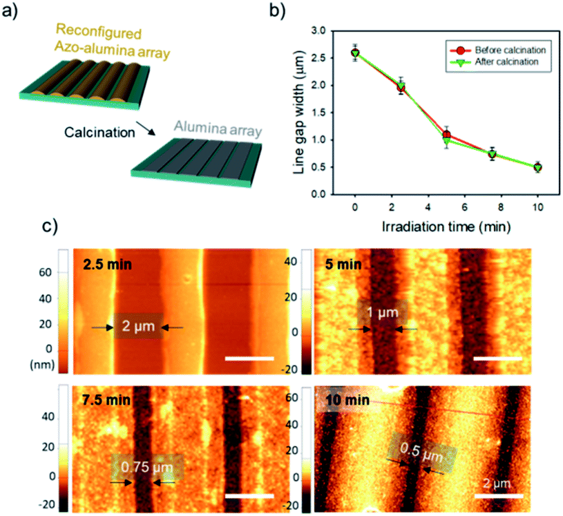 | ||
| Fig. 3 (a) Schematic diagram of the pyrolytic conversion of reconfigured azo–alumina line array. (b) The plots of the line gap width as a function of irradiation time before and after the pyrolytic conversion. (c) AFM images of the reconfigured line arrays with different irradiation time after the pyrolytic conversion. | ||
To confirm the conversion of the alumina precursor to alumina, we performed FT-IR analysis for the azopolymer, the azo–alumina composite, and the resulting alumina after the calcination. As seen in Fig. 4a, the IR spectrum of the un-calcined azo–alumina composite includes characteristic peaks of azopolymer, which can be clearly observed at 2700–3000 cm−1 (CH3), 1500 and 1600 cm−1 (aromatic ring), 1350–1450 cm−1 (–CH2 deformation), and 1330 cm−1 (C–N).35 In addition, the characteristic peaks of the chelated alumina precursor and slightly cross-linked alumina precursor were also observed at 1630–1700 cm−1 (C![[double bond, length as m-dash]](https://www.rsc.org/images/entities/char_e001.gif) O) and at 500–1000 cm−1 (Al–O–Al).36 The appearance of the Al–O–Al peak is probably attributed to unavoidable hydrolysis and condensation reaction of highly reactive aluminum tri-sec butoxide that even easily reacts with moisture in air. After the calcination at 500 °C for 1 h in air, all the peaks corresponding to organic components disappeared; the broad band centered at 3460 cm−1 from a superposition of vibration bands of bonded hydroxyl groups, isolated OH groups, and stretching vibrations of adsorbed water molecules, confirms the formation of γ-Al2O3.37 On the other hand, the Al–O–Al peak was significantly increased after the calcination, which demonstrates the conversion of azo–alumina to alumina. The quantitative analysis by EDX further supports the complete conversion. After the pyrolysis, the C and N signals from the organic moieties were substantially reduced to 0 atomic% as shown in Fig. 4b. Moreover, the O/Al atomic ratio after pyrolysis was close to that of pure alumina. Therefore, the FT-IR and EDX results cooperatively demonstrate the complete conversion of the azo–alumina composite to alumina.
O) and at 500–1000 cm−1 (Al–O–Al).36 The appearance of the Al–O–Al peak is probably attributed to unavoidable hydrolysis and condensation reaction of highly reactive aluminum tri-sec butoxide that even easily reacts with moisture in air. After the calcination at 500 °C for 1 h in air, all the peaks corresponding to organic components disappeared; the broad band centered at 3460 cm−1 from a superposition of vibration bands of bonded hydroxyl groups, isolated OH groups, and stretching vibrations of adsorbed water molecules, confirms the formation of γ-Al2O3.37 On the other hand, the Al–O–Al peak was significantly increased after the calcination, which demonstrates the conversion of azo–alumina to alumina. The quantitative analysis by EDX further supports the complete conversion. After the pyrolysis, the C and N signals from the organic moieties were substantially reduced to 0 atomic% as shown in Fig. 4b. Moreover, the O/Al atomic ratio after pyrolysis was close to that of pure alumina. Therefore, the FT-IR and EDX results cooperatively demonstrate the complete conversion of the azo–alumina composite to alumina.
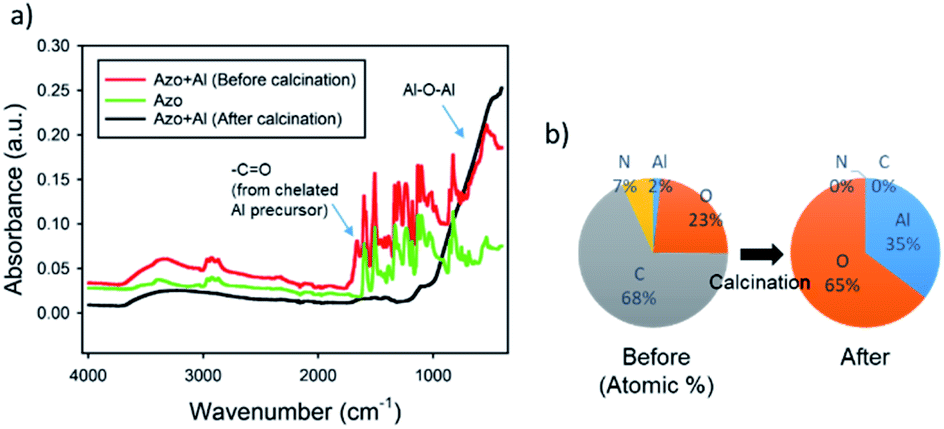 | ||
| Fig. 4 (a) FT-IR spectra of azopolymer and azo–alumina composite structure before and after calcination. (b) Elemental analysis of the azo–alumina composite before and after calcination. | ||
Conclusions
In this work, we developed a new platform for alumina-patterning based on the mixture of azobenzene polymer and chelated alumina precursor, which provides large flexibility in design layouts, structure reconfigurability and simple fab-process. Under far-field irradiation, the alumina precursor exhibited cooperative mass-migration with azobenzene polymer, therefore, the pre-patterned azo–alumina composite was deterministically reconfigured by adjusting irradiation time and light polarization. As a proof of concept, azo–alumina micro-line array was imprinted and reconfigured to have various gap-sizes through linearly polarized light irradiation. The photo-reconfigured azobenzene–alumina was completely converted to pure alumina through the two-step heat treatment, specially designed for a high structural fidelity. Based on its simplicity and efficacy in size and shape tuning, the proposed methods represent important progress toward more advanced use of alumina as a micro/nanolithographic tool.Conflicts of interest
There are no conflicts to declare.Acknowledgements
This work was supported by the KAIST Institute for Nano-Century (KINC).References
- X. Che, Y. He, H. Yin and L. Que, Biosens. Bioelectron., 2015, 72, 255–260 CrossRef CAS.
- I. Lauria, M. Kramer, T. Schröder, S. Kant, A. Hausmann, F. Böke, R. Leube, R. Telle and H. Fischer, Acta Biomater., 2016, 44, 85–96 CrossRef CAS PubMed.
- L. Treccani, M. Maiwald, V. Zöllmer, M. Busse, G. Grathwohl and K. Rezwan, Adv. Eng. Mater., 2009, 11, B61–B66 CrossRef.
- H. J. Lee, D. N. Kim, S. Park, Y. Lee and W.-G. Koh, Acta Biomater., 2011, 7, 1281–1289 CrossRef CAS PubMed.
- K. Endo and C. Adachi, Appl. Phys. Lett., 2014, 104, 121102 CrossRef.
- K. Tadanaga, N. Katata and T. Minami, J. Am. Ceram. Soc., 1997, 80, 3213–3216 CrossRef CAS.
- L. Li, J. Li, Y. Zhong, C. Chen, Y. Ben, J. Gong and Z. Ma, J. Mater. Chem., 2010, 20, 5446–5453 RSC.
- J. M. Kiyoharu Tadanaga and J. Tsutomu Minami, J. Sol-Gel Sci. Technol., 2000, 19, 211–214 CrossRef.
- M. Domanski, L. Winnubst, R. Luttge, E. Lamers, X. F. Walboomers, J. Jansen and H. Gardeniers, J. Mater. Sci.: Mater. Med., 2012, 23, 1637–1644 CrossRef CAS PubMed.
- S.-Y. Kim, J.-H. Kang, W.-S. Seo, S.-W. Lee, N.-S. Oh, H.-K. Cho and M.-H. Lee, Biomater. Res., 2015, 19, 23 CrossRef PubMed.
- N. Lim, Y. Pak, J. T. Kim, Y. Hwang, R. Lee, Y. Kumaresan, N. Myoung, H. C. Ko and G. Y. Jung, Nanoscale, 2015, 7, 13489–13494 RSC.
- Y. Iba, F. Kumasaka, H. Aoyama, T. Taguchi and M. Yamabe, Jpn. J. Appl. Phys., 1996, 35, 6463–6468 CrossRef CAS.
- J. Dekker, K. Kolari and R. L. Puurunen, J. Vac. Sci. Technol., B: Microelectron. Nanometer Struct.--Process., Meas., Phenom., 2006, 24, 2350–2355 CrossRef CAS.
- E. Zanchetta, G. D. Giustina, G. Grenci, A. Pozzato, M. Tormen and G. Brusatin, Adv. Mater., 2013, 25, 6261–6265 CrossRef CAS PubMed.
- M. D. Henry, S. Walavalkar, A. Homyk and A. Scherer, Nanotechnology, 2009, 20, 255305 CrossRef CAS PubMed.
- J. W. Lee, B. Pathangey, M. R. Davidson, P. H. Holloway, E. S. Lambers, B. Davydov, T. J. Anderson and S. J. Pearton, J. Vac. Sci. Technol., A, 1998, 16, 2177–2186 CrossRef CAS.
- C. Shin, T. Oh, T. J. Houlahan, C. H. Fann, S. J. Park and J. G. Eden, J. Phys. D: Appl. Phys., 2019, 52, 114001 CrossRef.
- S. Lee, H. S. Kang and J.-K. Park, Adv. Mater., 2012, 24, 2069–2103 CrossRef CAS.
- J. Choi, W. Cho, Y. S. Jung, H. S. Kang and H.-T. Kim, ACS Nano, 2017, 11, 1320–1327 CrossRef CAS.
- J. Choi, W. Jo, S. Y. Lee, Y. S. Jung, S.-H. Kim and H.-T. Kim, ACS Nano, 2017, 11, 7821–7828 CrossRef CAS PubMed.
- J. Choi, H. S. Kang, W. Jo, S.-H. Kim, Y. S. Jung and H.-T. Kim, Small, 2018, 14, 1703250 CrossRef.
- W. Jo, J. Choi, H. S. Kang, M. Kim, S. Baik, B. J. Lee, C. Pang and H.-T. Kim, ACS Appl. Mater. Interfaces, 2020, 12, 5058–5064 CrossRef CAS PubMed.
- M. J. Kim, S. J. Yoo and D. Y. Kim, Adv. Funct. Mater., 2006, 16, 2089–2094 CrossRef CAS.
- R. Nass and H. Schmidt, J. Non-Cryst. Solids, 1990, 121, 329–333 CrossRef CAS.
- H. Uchihashi, N. Tohge and T. Minami, J. Ceram. Soc. Jpn., 1989, 97, 396–399 CrossRef CAS.
- K. Y. Suh and R. Langer, Appl. Phys. Lett., 2003, 83, 1668–1670 CrossRef CAS.
- N. Tanaka, H. Moriguchi, A. Sato, T. Kawai, K. Shimba, Y. Jimbo and Y. Tanaka, RSC Adv., 2016, 6, 54754–54762 RSC.
- H. S. Kang, S. Lee and J.-K. Park, Adv. Funct. Mater., 2011, 21, 4412–4422 CrossRef CAS.
- S. Lee, H. S. Kang and J.-K. Park, Adv. Funct. Mater., 2011, 21, 1770–1778 CrossRef CAS.
- C. J. Barrett, A. L. Natansohn and P. L. Rochon, J. Phys. Chem., 1996, 100, 8836–8842 CrossRef CAS.
- H. S. Kang, H.-T. Kim, J.-K. Park and S. Lee, Adv. Funct. Mater., 2014, 24, 7273–7283 CrossRef CAS.
- B. Darracq, F. Chaput, K. Lahlil, Y. Lévy and J.-P. Boilot, Adv. Mater., 1998, 10, 1133–1136 CrossRef CAS.
- F. Chaput, D. Riehl, Y. Levy and J. P. Boilot, Chem. Mater., 1993, 5, 589–591 CrossRef CAS.
- O. Kulikovska, L. M. Goldenberg, L. Kulikovsky and J. Stumpe, Chem. Mater., 2008, 20, 3528–3534 CrossRef CAS.
- H. S. Kang, S. Lee, J. Choi, H. Lee, J.-K. Park and H.-T. Kim, ACS Nano, 2015, 9, 9837–9848 CrossRef CAS.
- Z. M. K. Majid Jafar Tafreshi, Mater. Sci., 2015, 21, 28–31 Search PubMed.
- T. Kawaharamura, T. Uchida, M. Sanada and M. Furuta, AIP Adv., 2013, 3, 032135 CrossRef.
Footnote |
| † Electronic supplementary information (ESI) available. See DOI: 10.1039/d0ra02931a |
| This journal is © The Royal Society of Chemistry 2020 |