
 Open Access Article
 This Open Access Article is licensed under a Creative Commons Attribution-Non Commercial 3.0 Unported Licence
High-performance ferroelectric non-volatile memory based on La-doped BiFeO3 thin films
Wanqiong Dai ,
Yuanxiang Li,
Caihong Jia,
Chaoyang Kang,
Mengxin Li and
Weifeng Zhang*
,
Yuanxiang Li,
Caihong Jia,
Chaoyang Kang,
Mengxin Li and
Weifeng Zhang*
Henan Key Laboratory of Photovoltaic Materials and Center for Topological functional materials, Henan University, Kaifeng 475004, China. E-mail: wfzhang6@163.com
First published on 11th May 2020
Abstract
An ultrathin (6.2 nm) ferroelectric La0.1Bi0.9FeO3 (LBFO) film was epitaxially grown on a 0.7 wt% Nb-doped SrTiO3 (001) single-crystal substrate by carrying out pulsed laser deposition to form a Pt/La0.1Bi0.9FeO3/Nb-doped SrTiO3 heterostructure. The LBFO film exhibited strong ferroelectricity and a low coercive field. By optimizing the thickness of the LBFO film, a resistance OFF/ON ratio of the Pt/LBFO (∼6.2 nm)/NSTO heterostructure of as large as 2.8 × 10⁵ was achieved. The heterostructure displayed multi-level storage and excellent retention characteristics, and showed stable bipolar resistance switching behavior, which can be well applied to ferroelectric memristors. The resistance switching behavior was shown to be due to the modulating effect of the ferroelectric polarization reversal on the width of the depletion region and the height of the potential barrier of the LaBiFeO3/Nb-doped SrTiO3 interface.
1. Introduction
Ferroelectric materials have recently attracted much attention due to the spontaneous polarization of ferroelectrics and the rapid reversal of electric drives. These materials are used in high-density and non-volatile ferroelectric random access memories with high write/read speeds, and have low levels of power consumption and other advantages.1 However, since ferroelectric materials are affected by interface size effects and since ultra-thin ferroelectric films easily depolarize,2–4 many ferroelectric random access memories use relatively thick ferroelectric layers. As a typical multiferroic material, bismuth ferrite (BFO) is a kind of lead-free ferroelectric material that displays many excellent properties, including a large residual ferroelectric polarization.2 Moreover, the narrow band gap of BFO results in relatively high leakage currents, which may also degrade the performance of its ferroelectric and interface-barrier-related properties.3 For example, Hu et al. demonstrated that the continuous tunable resistance switching behavior of Pt/BFO/NSTO heterostructures is due to polarization reversal, but its maximum resistance OFF/ON ratio is only 103.4 In order to improve the polarization-dependent performance of the device, a balance between ferroelectricity and conductivity must be found. Doping 10% La at the Bi position has been reported to be able to realize several changes in the crystal, including greatly reducing its quantity of Bi vacancies, improving its ferroelectricity, and stabilizing its structure, with these results due in part to the radii of La3+ and Bi3+, at 1.032 and 1.030 Å, being almost the same.5–7 The substitution of La3+ for Bi3+ has been shown to improve various aspects of the ferroelectric properties and structure of BFO, such as the coercive voltage, domain size and fatigue behavior.8,9 In this work, an ultra-thin LBFO film was used as the ferroelectric layer. By optimizing the thickness of the LBFO film, we achieved a Pt/LBFO/NSTO heterojunction that acts as a high-performance resistance switch, corresponding to ferroelectric polarization reversal.2. Experimental procedure
LBFO thin films were epitaxially grown on (001) single-crystal Nb-doped STO (Nb: 0.7% wt) substrates by performing pulsed laser deposition using a KrF excimer laser with a wavelength of 248 nm. The NSTO substrate was etched with a NH4F–HF-buffered solution prior to deposition of the LBFO film, and then annealed in O2 flowing at 950 °C for 1.5 h to form a TiO2 single-terminated step-terrace surface. The LBFO film was deposited using a laser with an energy density of 1.5 mJ cm−2 and repetition rate of 2 Hz, while maintaining the substrate temperature at 580 °C and an O2 pressure at 0.1 torr. After the film was deposited, it was annealed in situ for 10 min and then slowly cooled to room temperature at a rate of 6 °C min−1. The structure and crystal quality of the LBFO film were investigated using XRD (DX-2700). The film thickness was measured from X-ray reflection results. The surface morphology of the etched NSTO heterostructure was visualized using a Bruker Multimode 8 atomic force microscope. Atomic force microscopy (AFM), piezoelectric force microscopy (PFM), conductive atomic force microscopy (CAFM) and scanning Kelvin probe microscopy (SKPM) measurements were taken using an Asylum Research 3D Infinity instrument with a conductive Pt/Ti-coated tip as the top electrode. The resistance switchings of the Pt/LBFO/NSTO heterostructures were measured using a Keithley 2400 SourceMeter, the voltage pulse was supplied by using an arbitrary waveform generator (Agilent 33250A), the test pulse was applied to the Pt electrode, and the NSTO substrate was always grounded through an indium ohmic contact pad.3. Results and discussion
An XRD θ–2θ scan of the LBFO/NSTO heterostructure is shown in Fig. 1(a). The scan exhibited only the (001) and (002) diffraction peaks of the LBFO film. There was no other impurity phase and only one crystal direction of the film. In order to determine the thickness of the LBFO film, X-ray reflectance (XRR) measurements were taken of the sample, and the film thickness was calculated to be about 6.2 nm, as shown in Fig. 1(b). The surface topography of the etched NSTO is shown in Fig. 1(c). Flat atomic-level steps separated by ∼4 Å (single cells) were observed, as shown in the inset of Fig. 1(c). To assess the quality of the grown LBFO film, the surface morphology of the LBFO (∼6.2 nm)/NSTO heterostructure was visualized, as shown in Fig. 1(d). Its square root roughness was measured from this image to be 0.365 nm, confirming the excellent quality of the film.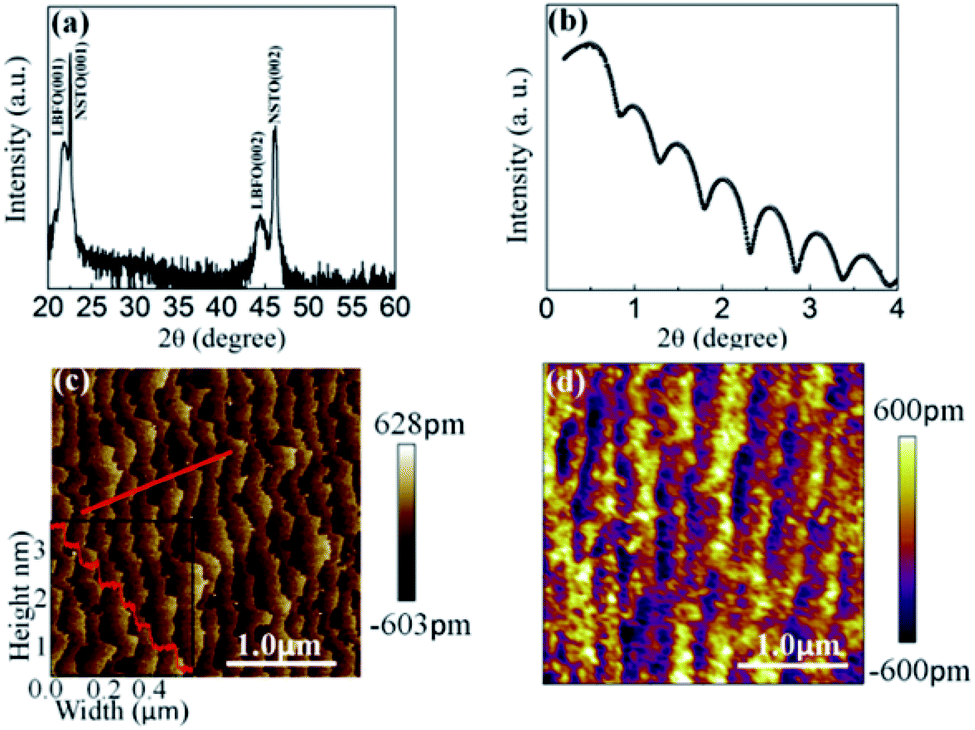 | ||
| Fig. 1 (a) XRD θ–2θ scan of the LBFO/NSTO (001) heterostructure. (b) X-ray reflectivity (XRR) measurements of the LBFO film. (c) Morphology of the etched NSTO. (d) Surface morphology of the 6.2 nm-thick LBFO layer grown on an NSTO substrate. | ||
We also carried out characterization of the LBFO film to investigate its ferroelectricity and resistance switching behavior, as shown in Fig. 2. Fig. 2(a) shows the pattern of voltage applied to the surface of the LBFO film. We used a piezoresponse force microscope (PFM) to investigate the ferroelectric properties of the LBFO films. Fig. 2(b) and (c) show the acquired PFM out-of-plane phase and PFM out-of-plane amplitude images acquired after applying −6 V and +6 V biases to the LBFO film surface. It can be seen from the figure that there is a significant polarization reversal in the area where the voltage is applied in the LBFO film, and the phase contrast is about 180°, implying that the LBFO film has excellent ferroelectricity. A local PFM measurement further showed an obvious phase lag and butterfly-like amplitude. As shown in Fig. 2(d), the coercive voltages, i.e., minimum values of the amplitude loop, were observed at about −3.0 and 2 V. In combination with PFM, we also studied the local current switching characteristics of the LBFO films using a conductive atomic force microscope (CAFM). Fig. 2(e) shows that when the LBFO was polarized at −6 V (+6 V), the center (outer) area showed a weaker (stronger) current, and the ferroelectric polarization was pointing away from (towards) the semiconductor substrate. This observation provided evidence for polarization-dependent resistance switching behavior occurring in the ferroelectric heterojunctions.10 We then characterized the LBFO membrane using a Kelvin probe force microscope (KPFM). Applying a negative (positive) bias to the LBFO film was predicted to attract positive (negative) ions and/or polarization charges to the surface, resulting in a lower (higher) surface potential.11 As shown in Fig. 2(f), our observations using this microscope were consistent with this prediction, demonstrating that the change in polarization charge was the primary effect. Therefore, ferroelectric polarization reversal can explain the resistance switching phenomenon exhibited in the LBFO/NSTO heterojunction, a relationship discussed in previous reports.12
 | ||
| Fig. 2 (a) Protocol for domain patterning. (b) PFM out-of-plane phase and (c) PFM out-of-plane amplitude images acquired after application of the domain patterning. (d) Phase and amplitude hysteresis loops for the LBFO/NSTO heterostructure. (e) Current and (f) SKPM images acquired after application of the domain patterning. | ||
In order to study the multi-level resistance switching and polarization switching behavior, we acquired an I–V curve from a Pt/LBFO/NSTO heterojunction with the device structure shown in the inset of Fig. 3(a). The positive direction of the current was defined as pointing from the top electrode to the bottom electrode, where the area of the top Pt electrode was 0.01 mm2. The voltage was applied in the order 0 V → +4 V → 0 V → −6 V → 0 V, with the arrows indicating the scanning direction, as shown in Fig. 3(a). The I–V curve was observed to exhibit a hysteresis behavior and asymmetry characteristics, which corresponded to resistance switching and rectification effects, respectively,13,14 and the device also exhibited a typical bipolar resistive switching (RS) behavior. In addition, with the application of different negative maximum voltage (−Vmax) levels, the Pt/LBFO/NSTO heterostructures exhibited a multi-level RS behavior. Here, as shown in Fig. 3(b), the voltage was applied in the order of 0 V → +4 V → 0 V→ −Vmax → 0 V. When −Vmax was set to −1 V, there was no significant RS window in the I–V curve. As the value of −Vmax was increased, the RS window increased and the device exhibited a multi-level RS effect.
 | ||
| Fig. 3 (a) I–V curves of the Pt/LBFO/NSTO heterostructure on a semi-log scale. The inset shows the structure of the device used for the measurement. (b) Multilevel RS behavior of the heterostructure. (c) A typical R–V hysteresis loop and corresponding RS multilevel effect of the LBFO heterostructure at room temperature. (d) Pulsed-read R–V loops with the scanning directions illustrated by arrows. (e) Room-temperature pulsed-read R–V loops of the Pt/LBFO/NSTO heterostructures with 6.2, 9.3 and 18.6 nm-thick LBFO layers. The scanning directions are illustrated by arrows. | ||
To better understand the traditional bipolar resistance switching and multi-level RS behavior observed in the I–V loop, pulse R–V measurements were further taken to study the non-volatile resistance switching (RS) behavior. During the R–V measurements, write pulses at various voltages and read pulses of −0.2 V were alternately applied. Fig. 3(c) shows a typically acquired R–V hysteresis loop at room temperature, which clearly illustrated the RS multilevel effect of the LBFO heterostructure. By changing the applied voltage pulse, we were able to continuously tune the resistance over a range of several orders of magnitude, and the hysteresis change of the resistance with the applied voltage was basically the same as that of the electromagnetic hysteresis loop, which indicated that the resistance switching behavior was caused by a ferroelectric polarization reversal.4 Moreover, the transition voltages observed in the I–V and R–V loops corresponded basically to the coercive voltages observed in the PFM phase and amplitude curves, also indicating that ferroelectric polarization directly controls the interface barrier. The RS window tended to saturate with increasing write pulse amplitude, with a maximum of 2.8 × 10⁵ (see Fig. 3(d)). The large ratio observed here was approximately 100 times those of the reported Pt/LBFO/NSTO heterostructure4 and Pt/LBFO/SRO heterojunction,15 due to the modulating effect of the ferroelectric polarization reversal on the LBFO/NSTO interface. In order to balance the conductivity and ferroelectricity, we needed to find the proper thickness of the LBFO layer. Fig. 3(e) shows the R–V hysteresis loop results for devices with different LBFO film thicknesses. Compared with the LBFO films that have thicknesses of 9.3 and 18.6 nm, that with a thickness of 6.2 nm LBFO showed a greater resistive switching ratio and slightly weaker coercive fields. That is, we found that the resistive switching ratio decreased with increasing LBFO thickness. The LRS state resistance clearly exhibited only a slight variation, while the HRS state resistance decreased by about 1.5 orders of magnitude as the LBFO thickness was increased from 6.2 to 18.6 nm. This result may have been due to the previously noted effect of thickness on electric-field-induced domain switching in such types of ferroelectric thin films16 and the incomplete shielding of the charge depolarization field generated in the ferroelectric thin film.17 It is worth noting that the Pt/LBFO/NSTO heterostructure exhibited a large switching ratio related to ferroelectric polarization, and the modulation voltage was greatly reduced.3,4,18
For practical applications of non-volatile memories, the most important features that they should display are a large resistance OFF/ON ratio, long hold time, and stable fatigue characteristics. We investigated the LBFO/NSTO heterostructure with the LRS and HRS written using pulses of +4 V and −6 V, respectively, and took measurements with a Vread of −0.2 V. As shown in Fig. 4(a), the device showed excellent retention of resistance, and no significant degradation was observed after about 10 h in both the ON and OFF states. After more than 105 write/read cycles, no significant change in OFF/ON ratio was observed, and the device still maintained a large OFF/ON ratio, as shown in Fig. 4(b). Furthermore, the non-volatility of the bipolar switch was monitored, as shown in Fig. 4(c), and it displayed excellent retention during cycling. The device performance was comparable to that obtained for the Pt/BFO/NSTO heterostructures reported by Hu4 and Wang.19
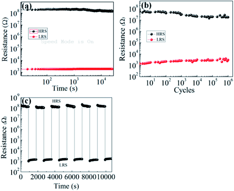 | ||
| Fig. 4 (a) Retention, (b) cycling, and (c) cycling retention of the LBFO/NSTO heterostructure with the LRS and HRS written by applying pulses of +4 V and −6 V, respectively. | ||
Based on the above detailed analysis, a modulating effect of the ferroelectricity polarization on the width of the depletion region and the barrier height at the LBFO/NSTO interface can be used to explain the resistance switching behavior observed in the heterostructure.20 Upon applying a positive write voltage pulse (+4 V) to the device, the LBFO film would become polarized downward and the positive polarization bound charges would accumulate at the LBFO/NSTO interface. As a result of the ferroelectric field effect,21 as shown in Fig. 5(a), the positive polarization-bound charges would attract most of the negative electron carriers in the n-type NSTO to move to the interface, thereby reducing the width of the depletion layer. In contrast, as shown in Fig. 5(b), upon applying a negative write voltage pulse (−6 V) to the device, most of the negative electron carriers in the n-type NSTO would be repelled by the negative polarization bound charges away from the interface, increasing the width of the depletion layer. In addition, due to the shielding of the bound charge being generally incomplete, a depolarizing field opposite to the direction of polarization would be generated in the ferroelectric layer,17 resulting in a bent band at the interface,22 as shown in the band diagram of the Pt/LBFO/NSTO heterostructure in Fig. 5(a) and (b). Therefore, the resistive switching behavior in the heterostructure can be explained by the modulating effect of ferroelectric polarization on the depletion width and barrier height of the LBFO/NSTO interface.
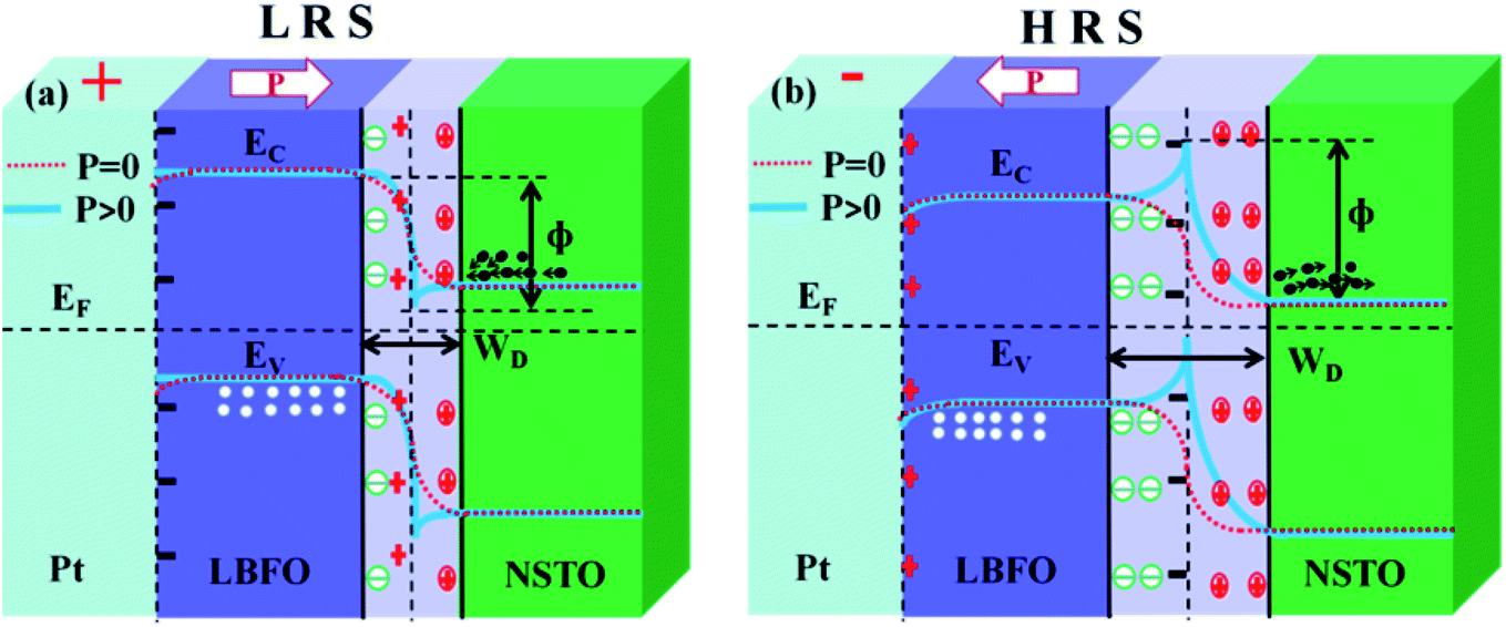 | ||
| Fig. 5 Schematic diagrams of the Pt/LBFO/NSTO heterostructure energy band diagrams at (a) LRS and (b) HRS. Circles with a “−” in the center indicate acceptor, circles with a “+” in the center indicate donor, the symbol “+” represents positive bound charge, and “−” represents negative bound charge. White circles and black dots represent holes and electrons, respectively. | ||
4. Conclusions
In summary, epitaxial LBFO ferroelectric thin films were grown on Nb-doped SrTiO3 substrates by performing pulsed laser deposition to form Pt/LBFO/NSTO heterojunctions. They showed stable bipolar resistance switching characteristics, and a maximum ROFF/RON ratio of 2.8 × 10⁵, with good retention and multi-level storage characteristics, which were attributed to a modulation of the depletion width and barrier height of the LBFO/NSTO interface as a result of ferroelectric polarization. The advantages of the ferroelectric heterojunction in terms of retention, durability, multi-level storage and repeatability are beneficial for use in novel non-volatile multi-functional memories.Conflicts of interest
There are no conflicts to declare.Acknowledgements
This work was supported by the National Natural Science Foundation of China (Grant No. 11974099).References
- J. F. Scott, Science, 2007, 315, 954–959 CrossRef CAS PubMed.
- A. Q. Jiang, C. Wang, K. J. Jin, X. B. Liu, J. F. Scott, C. S. Hwang, T. A. Tang, H. B. Lu and G. Z. Yang, Adv. Mater., 2011, 23, 1277–1281 CrossRef CAS PubMed.
- L. Pintilie, C. Dragoi, Y. H. Chu, L. W. Martin, R. Ramesh and M. Alexe, Appl. Phys. Lett., 2009, 94, 232902 CrossRef.
- Z. Hu, Q. Li, M. Li, Q. Wang, Y. Zhu, X. Liu, X. Zhao, Y. Liu and S. Dong, Appl. Phys. Lett., 2013, 102, 102901 CrossRef.
- Y.-H. Chu, Q. He, C.-H. Yang, P. Yu, L. W. Martin, P. Shafer and R. Ramesh, Nano Lett., 2009, 9, 1726–1730 CrossRef CAS PubMed.
- P. Maksymovych, J. Seidel, Y. H. Chu, P. Wu, A. P. Baddorf, L. Q. Chen, S. V. Kalinin and R. Ramesh, Nano Lett., 2011, 11, 1906–1912 CrossRef CAS PubMed.
- M. X. Zhou, B. Chen, H. B. Sun, J. G. Wan, Z. W. Li, J. M. Liu, F. Q. Song and G. H. Wang, Nanotechnology, 2013, 24, 225702 CrossRef PubMed.
- Y.-H. Lee, J.-M. Wu and C.-H. Lai, Appl. Phys. Lett., 2006, 88, 042903 CrossRef.
- Y. H. Chu, Q. Zhan, C. H. Yang, M. P. Cruz, L. W. Martin, T. Zhao, P. Yu, R. Ramesh, P. T. Joseph, I. N. Lin, W. Tian and D. G. Schlom, Appl. Phys. Lett., 2008, 92, 102909 CrossRef.
- C. Jia, J. Li, G. Yang, Y. Chen and W. Zhang, Nanoscale Res. Lett., 2018, 13, 102 CrossRef PubMed.
- Z. Fan, H. Fan, L. Yang, P. Li, Z. Lu, G. Tian, Z. Huang, Z. Li, J. Yao, Q. Luo, C. Chen, D. Chen, Z. Yan, M. Zeng, X. Lu, X. Gao and J.-M. Liu, J. Mater. Chem. C, 2017, 5, 7317–7327 RSC.
- X. Chen, C. H. Jia, Y. H. Chen, G. Yang and W. F. Zhang, J. Phys. D: Appl. Phys., 2014, 47, 365102 CrossRef.
- T. L. Qu, Y. G. Zhao, D. Xie, J. P. Shi, Q. P. Chen and T. L. Ren, Appl. Phys. Lett., 2011, 98, 173507 CrossRef.
- S. Y. Yang, L. W. Martin, S. J. Byrnes, T. E. Conry, S. R. Basu, D. Paran, L. Reichertz, J. Ihlefeld, C. Adamo, A. Melville, Y.-H. Chu, C.-H. Yang, J. L. Musfeldt, D. G. Schlom, J. W. Ager and R. Ramesh, Appl. Phys. Lett., 2009, 95, 062909 CrossRef.
- D. Li, D. Zheng, C. Jin, W. Zheng and H. Bai, ACS Appl. Mater. Interfaces, 2018, 10, 19836–19843 CrossRef CAS PubMed.
- G. Cao, H. Huang and X. Ma, Appl. Sci., 2017, 7, 1162 CrossRef.
- R. R. Mehta, B. D. Silverman and J. T. Jacobs, J. Appl. Phys., 1973, 44, 3379–3385 CrossRef CAS.
- C. Wang, K.-j. Jin, Z.-t. Xu, L. Wang, C. Ge, H.-b. Lu, H.-z. Guo, M. He and G.-z. Yang, Appl. Phys. Lett., 2011, 98, 192901 CrossRef.
- L. Wang, K.-j. Jin, C. Ge, C. Wang, H.-z. Guo, H.-b. Lu and G.-z. Yang, Appl. Phys. Lett., 2013, 102, 252907 CrossRef.
- R. Meyer and R. Waser, J. Appl. Phys., 2006, 100, 51611 CrossRef.
- S. Mathews, R. Ramesh, T. Venkatesan and J. Benedetto, Science, 1997, 276, 238–240 CrossRef CAS PubMed.
- Y. Watanabe, Phys. Rev. B: Condens. Matter Mater. Phys., 1999, 59, 11257 CrossRef CAS.
| This journal is © The Royal Society of Chemistry 2020 |