 Open Access Article
An inverted ZnO/P3HT:PbS bulk-heterojunction hybrid solar cell with a CdSe quantum dot interface buffer layer†
Ajith Thomasab,
R. Vinayakanc and
V. V. Ison *a
*a
aCentre for Nano-Bio-Polymer Science and Technology, Research and PG Department of Physics, St. Thomas College Palai, Kerala – 686574, India. E-mail: isonv@rediffmail.com; Tel: +919446126926
bResearch and Development Centre, Bharathiar University, Coimbatore, Tamilnadu – 641046, India
cNSS Hindu College Changanacherry, Kottayam-686102, Kerala, India
First published on 28th April 2020
Abstract
An inverted bulk-heterojunction (BHJ) hybrid solar cell having the structure ITO/ZnO/P3HT:PbS/Au was prepared under ambient conditions and the device performance was further enhanced by inserting an interface buffer layer of CdSe quantum dots (QDs) between the ZnO and the P3HT:PbS BHJ active layer. The device performance was optimized by controlling the size of the CdSe QDs and the buffer layer thickness. The buffer layer, with an optimum thickness and QD size, has been found to promote charge extraction and reduces interface recombinations, leading to an increased open-circuit voltage (VOC), short circuit current density (JSC), fill factor (FF) and power conversion efficiency (PCE). About 40% increase in PCE from 1.7% to 2.4% was achieved by the introduction of the CdSe QD buffer layer, whose major contribution comes from a 20% increase of VOC.
Introduction
Third-generation solar cells such as conjugated polymer solar cells, quantum dot (QD) based organic and inorganic solar cells, dye-sensitized solar cells and perovskite solar cells have received considerable research interest in the past few decades due to their advantages like mechanical flexibility and cost-effectiveness in fabricating large-area solar cells from solution phase.1–5 Among these, the polymer based bulk-heterojunction (BHJ) solar cells, in which the fullerene derivatives are replaced with QDs, grabbed much attention because of their exceptional features like tunable band gap, low specific weight, wide spectral range absorption and excellent photostability.6 Cadmium chalcogenide QDs are the first material to replace the fullerene derivatives in polymer-based BHJ hybrid solar cells.7,8 This, along with the device optimizations resulted in significant improvement in the power conversion efficiency (PCE) and long term stability of these devices.9–11 But, a bottleneck with the cadmium based QDs is their absorption window, limited to the UV-visible region of the solar spectrum, that further led to the exploration of NIR absorbing lead chalcogenide QDs. Lead chalcogenide QDs have an additional scope for multiple exciton generation (MEG) by solar photons and a resulting hot carrier extraction.12–14Lead sulphide (PbS) QDs in combination with poly(3-hexylthiophene) (P3HT) is one of the most studied BHJ systems by several research groups.15 In a typical stack, a P3HT:PbS active layer is sandwiched between a hole transporting poly(3,4-ethylenedioxylthiophene):poly(styrenesulfonate) (PEDOT:PSS)) layer on indium doped tin oxide (ITO) and a low work function metal cathode.16–18 But, the cell stability issues caused by the inherent acidic and hygroscopic nature of PEDOT:PSS demanded new structures avoiding its use. An alternative technique emerged then was an inverted architecture employing a cathode buffer layer, for example a zinc oxide (ZnO) layer. Though the inverted structures were widely explored in organic solar cells,19,20 only few attempts were performed in polymer/QD hybrid solar cells.21,22
In this paper, we report the fabrication of an inverted P3HT:PbS BHJ hybrid solar cell with the structure ITO/ZnO/P3HT:PbS/Au. A layer of ZnO nanocrystals is used as an electron transporting medium in the cell structures fabricated. ZnO has been used as an electron transport layer in QD solar cells (QDSC), organic solar cells and hybrid solar cells extensively. Features like high electron mobility, chemical stability, ease of synthesis and good transparency across the visible spectral range make ZnO an electron acceptor, a hole blocking layer and a buffer layer in photovoltaics.19–22 But ZnO has a major disadvantage that it possess a large density of surface trap states, which deteriorates the cell performance through interface carrier recombination.19,20 In the device structure that we have explored, since ZnO makes junctions with both P3HT and PbS in the BHJ active layer, the effects of the interface recombination of electrons through the interband trap states of ZnO to the valence band of both P3HT and PbS is a major concern. The possible strategies to overcome the issue would be like the doping of the ZnO layer, introduction of an interface buffer layer between the active layer and ZnO, etc.20,23–25 In this work, we have explored the second option, i.e., the introduction of a buffer layer. A cadmium selenide (CdSe) QDs layer was found to be ideal in our case because of its energy band structure that lie intermediate between ZnO and the BHJ active layer. The CdSe QDs layer would then act as an energy relay in the active layer/ZnO interface mediating an efficient electron transfer to the ZnO layer.25,26 Optimizations were done for the QDs size and the buffer layer thickness for improving the cell performance. The QDs were characterized using optical absorption, photoluminescence (PL) and High-Resolution Transmission Electron Microscopy (HR-TEM). The performance of the cell structures were evaluated using a source meter utilizing a solar simulator and the external quantum efficiency (EQE) measurements. Fourier Transform Infrared Spectroscopy (FTIR), Ultraviolet Photoelectron Spectroscopy (UPS) and Cross-sectional Scanning Electron Microscopy (Cr-SEM) were carried out to complement the primary characterizations.
Experimental
Materials
Regioregular P3HT was obtained from Rieke Metals. ITO coated glass substrates (8–12 Ω sq−1), lead(II) oxide (PbO, 99.999%, trace metals basis), cadmium oxide (CdO, ≥99.99%, trace metals basis), trioctylphosphine (TOP, technical grade, 90%), hexamethyldisilathiane (TMS, Synthesis Grade), selenium (Se, 99.99%, trace metals basis), oleic acid (OA, technical grade 90%), 1-octadecene (1-ODE, technical grade 90%), 1,2-ethanedithiol (EDT, ≥98% GC), zinc acetate dihydrate (ACS reagent, ≥98%), potassium hydroxide (KOH basis ≥ 85%), n-octane (anhydrous, ≥99%) were purchased from Sigma Aldrich. Reagents and solvents were purchased from Merck. All the chemicals were used as such without further purification.Synthesis of ZnO nanocrystals
Zinc acetate dihydrate (1.515 g, 6.9 mmol) was dissolved in methanol (65 ml) in a 100 ml three-necked round bottom flask and was heated to 60 °C under argon atmosphere. After 30 minutes, KOH (0.726 g, 12.9 mmol) in methanol (34 ml) was injected drop-wise into the mixture in a time interval of 10 minutes. The solution turned translucent initially during the injection and became transparent slowly. 90 minutes after the completion of the injection, ZnO nanocrystals (NCs) started precipitating and the solution became turbid. After 2 hours of the injection, the mixture was cooled down to room temperature and was kept undisturbed for 6 hours for the ZnO nanocrystals to sediment at the bottom. After removing the supernatant, 30 ml methanol was added to the precipitate and stirred again. The NCs were precipitated by centrifuging at 1000 rpm for 4 minutes and redispersed in 30 ml methanol. The centrifugation was repeated further at 4000 rpm and finally after removing the residual methanol, the ZnO NCs were dispersed in chloroform with a weight concentration of 30 mg ml−1 and filtered through a 0.2 μm polytetrafluoroethylene (PTFE) filter.Synthesis of PbS and CdSe QDs
PbS and CdSe QDs were synthesised by hot-injection method. For synthesising PbS QDs capped with OA, a pot mixture of PbO (1.2 g, 5.4 mmol), OA (11 ml, 35 mmol) and ODE (32.3 ml, 101 mmol) was loaded into a 3-neck round bottom flask equipped with a thermometer, condenser and a rubber septum. The mixture was heated to 150 °C and kept for stirring for 1 hour followed by degassing at 100 °C before the temperature reaches 150 °C. An injection mixture was also prepared simultaneously by mixing TMS (500 μl, 2.37 mmol) with ODE (19 ml, 59 mmol) in a round bottom flask. After 1 hour, the temperature of the pot mixture was reduced to 130 °C followed by a swift injection of the degassed injection mixture to initiate the growth of the PbS QDs. It was then held for a minute to attain the required size and cooled down to room temperature using a cold water bath. 15 ml hexane was added to the crude solution containing QDs to disperse them and was precipitated with acetone followed by centrifugation. The QDs, dried under vacuum were dispersed in hexane again and were further precipitated with methanol and the steps were repeated twice. The purified QDs were finally dispersed in a 2![[thin space (1/6-em)]](https://www.rsc.org/images/entities/char_2009.gif) :
:![[thin space (1/6-em)]](https://www.rsc.org/images/entities/char_2009.gif) 1 chloroform-chlorobenzene mixture at a concentration of 50 mg ml−1.
1 chloroform-chlorobenzene mixture at a concentration of 50 mg ml−1.
The pot mixture for synthesizing OA capped CdSe QDs was prepared by dissolving 400 mg of CdO (3.1 mmol), 55 ml ODE (170 mmol) and 4.8 ml OA (15.3 mmol) in a three-necked round-bottom flask. The injection mixture was prepared by dissolving 80 mg (1 mmol) of Se powder in 770 μl (1.7 mmol) TOP and 6.7 ml (21 mmol) ODE. Rest of the procedures were similar to that for PbS QDs, except the injection temperature and the growth time. CdSe QDs of three different sizes viz., 2.9 nm, 4 nm and 7 nm were synthesized by adjusting the growth temperature at 280 °C, 300 °C and 320 °C, respectively. The growth time was maintained 3 minutes in all the cases. 6 ml hexane was added to the crude solution to disperse the QDs and was precipitated by adding excess methanol followed by centrifugation at 6000 rpm. The QDs were dried under vacuum and dispersed in 3 ml of hexane again. The precipitation procedures were repeated thrice and the vacuum-dried powder of QDs was dispersed in chlorobenzene (CB) at a concentration 30 mg ml−1 for spin coating.
The PbS and CdSe QDs dispersions were filtered through a 0.22 μm PTFE filter. The characterizations of the QDs are shown in the ESI (Fig. S1 and S2†).
Device fabrication
Patterned ITO coated glasses were cleaned following our previously reported procedure.27 A 60 nm ZnO layer was formed on it by spin-coating the ZnO solution for 30 seconds at 3000 rpm. The film was then annealed at 230 °C for 20 minutes on a hot plate. On ZnO, the CdSe buffer layer was grown by spin-coating the CdSe dispersion for 30 seconds at 2000 rpm. The parameters of spin-coating, the spin speed and the concentration of the coating solution, were initially optimized to get a CdSe film thickness around 20 nm. 200 μl EDT solution (0.02% volume in acetonitrile) was applied to the spin-coated film for the ligand exchange process for 30 seconds. The film was then rinsed with pure acetonitrile for removing excess ligands while the substrate was spinning (for 10 seconds at 500 rpm). Acetonitrile was again applied to the film and dried by spinning at 3000 rpm. CdSe buffer layers were also grown for thicknesses 40 nm and 60 nm by repeating the deposition cycle.For the fabrication of the BHJ active layer P3HT:PbS, the PbS dispersion was blended with P3HT solution (10 mg ml−1 in 2![[thin space (1/6-em)]](https://www.rsc.org/images/entities/char_2009.gif) :
:![[thin space (1/6-em)]](https://www.rsc.org/images/entities/char_2009.gif) 1 chloroform–chlorobenzene) to form a 1
1 chloroform–chlorobenzene) to form a 1![[thin space (1/6-em)]](https://www.rsc.org/images/entities/char_2009.gif) :
:![[thin space (1/6-em)]](https://www.rsc.org/images/entities/char_2009.gif) 9 (w/w) polymer-QDs solution. Before spin coating, a small amount of octane (10% v/v) was added as a solvent additive to the casting solution based on our earlier work on optimizing BHJ morphology of P3HT:PCBM solar cells.27
9 (w/w) polymer-QDs solution. Before spin coating, a small amount of octane (10% v/v) was added as a solvent additive to the casting solution based on our earlier work on optimizing BHJ morphology of P3HT:PCBM solar cells.27
The active layer was spin-coated for 40 seconds at 1500 rpm to get a film of thickness 140 nm. The device structures were heated at 120 °C for 10 minutes before the final Au electrode deposition. All the fabrication procedures were carried out under ambient conditions.
Characterizations
The absorption spectra of the QDs dispersions in hexane were recorded using an Agilent Cary 5000 UV-Vis-NIR Spectrophotometer. The absorptances of the active layers were measured from the devices prepared without electrode deposition. Photoluminescence (PL) spectra of CdSe QDs were recorded using a HORIBA Fluorolog-3 spectrometer. Fourier Transform Infrared Spectra (FTIR) of CdSe QDs (4 nm) layer with and without EDT treatment were obtained with a Nicolet iS20 FTIR Spectrometer in the ATR mode. The EDT capped CdSe sample was prepared by spin-coating CdSe QDs (4 nm size) layers on a glass substrate 6 times with EDT treatments in between. High-Resolution Transmission Electron Microscope (HR-TEM) images of the QDs were recorded using a JEOL JEM-2100 microscope. For HR-TEM studies, the QDs dispersions in hexane were drop-casted on copper grid. Cross-sectional Scanning Electron Microscope (Cr-SEM) images of the devices were taken using a Zeiss Sigma 300 SEM. The thicknesses of all layers in the devices were measured using the Cr-SEM. Photovoltaic performances of the devices were recorded using a Keithley 2400 source meter under ambient conditions. An Oriel Sol3A Class AAA solar simulator was used to provide a 100 mW cm−1 (ref. 2) light illumination. A series of neutral density filters were used to study the illumination intensity dependence of JSC and VOC. External quantum efficiency (EQE) spectra of the devices were taken using a BENTHAM PVE300 IPCE measurement system. Ultraviolet Photoelectron Spectroscopy (UPS) analysis of EDT capped CdSe QDs film was performed using a Kratos AXIS ULTRA system equipped with a He I radiation source (21.22 eV). The sample for the UPS analysis was prepared by coating two layer of EDT treated CdSe QDs films on a silicon wafer.Results and discussion
In this communication, we report a novel inverted P3HT:PbS BHJ hybrid solar cell with the structure ITO/ZnO/P3HT:PbS/Au employing ZnO as the electron transporting layer. The device performance was further improved by integrating a CdSe QDs interface buffer layer to form the structure ITO/ZnO/CdSe/P3HT:PbS/Au. The CdSe and the BHJ layers were subjected to post-deposition ligand exchange processes to replace the long and insulating OA ligands with shorter EDT ligands. The ligand exchange process was validated by FTIR studies. A nearly complete removal of OA was seen after EDT treatment indicated by a significant reduction of the characteristic vibrations at 2920 cm−1 (asymmetric C–H) and 2850 cm−1 (symmetric C–H) in the FTIR spectra (Fig. S3†).28Fig. 1a shows the Cr-SEM image of a device grown with CdSe buffer layer. A schematic of the device is shown in Fig. 1b.
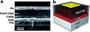 | ||
| Fig. 1 (a) Cross-sectional SEM image of the inverted structure ITO/ZnO/CdSe/P3HT:PbS/Au and (b) schematic of the device. | ||
Initially, CdSe QDs of three different sizes (2.9 nm, 4 nm and 7 nm) were explored for fabricating cell structures at a buffer layer thickness around 40 nm and it was found that the device grown with 4 nm QDs gave the maximum photo conversion efficiency (PCE). Now, using the 4 nm CdSe nanoparticles, cells were grown at three buffer layer thicknesses, ∼20 nm, ∼40 nm and ∼60 nm and the device with a 20 nm buffer layer provided the best results. A summary of the photovoltaic (PV) parameters of the devices with QDs size and the buffer layer thickness is given in Table 1 and 2 respectively. The parameters tabulated correspond to average of 4 devices each having 8 cells. A photograph of our typical device is shown in the inset in Fig. 2.
| QD size (nm) | VOC (V) | JSC (mA cm−2) | FF (%) | PCE (%) |
|---|---|---|---|---|
| 2.9 | 0.63 ± 0.02 | 6.20 ± 0.9 | 43.5 ± 2.2 | 1.7 ± 0.2 |
| 4 | 0.60 ± 0.01 | 7.40 ± 0.5 | 47.0 ± 1.8 | 2.1 ± 0.2 |
| 7 | 0.58 ± 0.01 | 7.00 ± 0.3 | 47.6 ± 1.3 | 1.9 ± 0.1 |
| CdSe layer thickness (nm) | VOC (V) | JSC (mA cm−2) | FF (%) | PCE (%) |
|---|---|---|---|---|
| 20 | 0.61 ± 0.02 | 7.75 ± 0.7 | 50.2 ± 2.2 | 2.4 ± 0.2 |
| 40 | 0.60 ± 0.01 | 7.40 ± 0.5 | 47.0 ± 1.8 | 2.1 ± 0.2 |
| 60 | 0.57 ± 0.01 | 7.18 ± 0.6 | 44.9 ± 1.4 | 1.8 ± 0.1 |
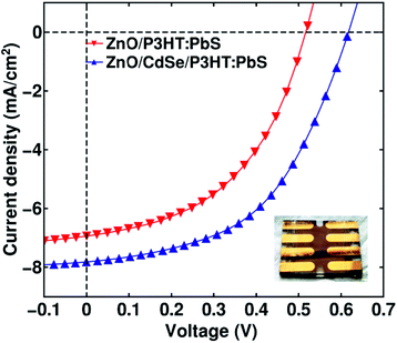 | ||
| Fig. 2 J–V characteristics under illumination for the devices with and without CdSe buffer layer. Inset shows photograph of a typical device. | ||
Fig. 2 shows the current density–voltage (J–V) characteristics of the best-performed devices, with and without the CdSe buffer layer (20 nm layer formed of 4 nm QDs).
The charge transport mechanism in inverted BHJ hybrid solar cells is well understood.15 In the bulk of a P3HT:PbS active layer, the photo-generated electron–hole pairs in P3HT and PbS QDs are separated at the P3HT:PbS interfaces and get collected at PbS QDs and P3HT respectively due to the favourable band alignment between them. At the active layer/ZnO interface, the electrons collected in PbS along with some of the excited electrons in the P3HT are transferred to the ZnO layer since the electron transfer from the PbS and the P3HT to the ZnO is efficient.20,29 The mechanism is also similar in PbS quantum dot solar cells and P3HT based inverted BHJ solar cells, where ZnO acts as an electron transport layer. But, since the ZnO/active layer (PbS QDs in QDSCs and BHJ layer in P3HT based polymer solar cells) interface is prone to interface recombination due to the surface states present at the ZnO surface,20,29 a deteriorated device performance results mainly from an inferior VOC and a lower FF. The present study is centred on overcoming this issue by growing a CdSe QDs surface passivation buffer layer to reduce the interface recombination.25,29 Significant improvements are reflected in the performance of the devices grown with the buffer layer (CdSe/P3HT:PbS), especially a 20% increase in VOC, as compared to the devices grown without buffer layer (P3HT:PbS). A comparison of the PV parameters of the devices grown with and without the buffer layer is given in Table 3.
| Devices | VOC (V) | JSC (mA cm−2) | FF (%) | PCE (%) |
|---|---|---|---|---|
| ZnO/P3HT:PbS | 0.51 ± 0.01 | 6.90 ± 0.5 | 46.9 ± 1.8 | 1.7 ± 0.2 |
| ZnO/CdSe/P3HT:PbS | 0.61 ± 0.02 | 7.75 ± 0.7 | 50.2 ± 2.2 | 2.4 ± 0.2 |
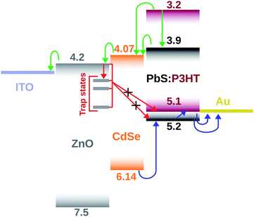
The reason for utilising CdSe QDs as the interface buffer layer is its well-matched conduction band edge to ZnO and the BHJ active layer components, providing an intermediate energy level between them, promoting electron transport to ZnO. The enhanced electron transport reduces the interface charge density that further results in a reduction of the interface charge recombination.24,25 To illustrate the charge carrier transportation and recombination pathways, an energy band diagram is constructed, which is shown in Fig. 3.
All energy level positions were taken from the previously reported studies except the one for EDT capped CdSe QDs. For CdSe QDs, since the energy level positions depend very much on their surface capping ligands and the band gap, the energy level positions were obtained from UPS and PL measurements.30 The UPS characterization details are provided in Fig. S4.†
The energy level positions of all constituting layers of the device are given in Table S2.† In the energy band diagram, the green and the blue arrows denote the electron and hole transportation pathways respectively and the red arrows depict the major interface recombination pathways. The recombinations to PbS and P3HT are mediated by the trap states on the ZnO surface. The deep-lying HOMO level of CdSe prevents holes in the HOMO of both P3HT and PbS from getting in contact with the ZnO surface.
To get more information on the recombination kinetics in the devices, we analysed how JSC and VOC depend on the light intensity I. Fig. 4 shows the dependence of JSC on light intensity (the curve is plotted on a double logarithmic scale). The data was then fitted with a power-law based on the proportionality JSC∝Iγ, where γ is an exponential factor, whose value can be used to interpret the carrier recombination mechanism in the devices under short circuit condition. If the γ value is close to 1, it suggests that the carrier extraction is faster than recombination in the devices and so that it possess very little bimolecular recombination under short circuit condition or may be dominated by monomolecular recombination. A lower value of γ (∼0.5) is indicative of bimolecular recombination processes in the device.31,32 In our study, we have obtained a γ value equal to 0.78 for the device grown with buffer layer and a value 0.74 for the one without buffer. A higher value of γ for the device with buffer layer as compared to the device without buffer is in favour of our argument that there occurs a reduction in the interface charge carrier density and the associated bimolecular recombination with the introduction of the buffer layer.24,25,32
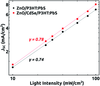 | ||
| Fig. 4 Dependence of JSC on light intensity for the devices grown with and without CdSe buffer layer. | ||
Determination of ideality factor η is another route to assess the recombination processes in solar cells. Fig. 5 shows the variation of VOC on light intensity plotted on a logarithmic scale. The ideality factor can be obtained by fitting the data using the relation VOC = (ηkT/q)ln(Iγ) + C where, k is the Boltzmann constant, T is the absolute temperature, q is the elementary charge and C is a constant. The ideality factor gives the value 1 when there is only band-to-band recombination in the open-circuit condition. Its value will be in the range 1 to 2 when the trap assisted recombination from interface or mid-gap states dominates.32–34 The ideality factor calculated for our cases with (1.76) and without buffer (2.22) indicates that the trap assisted recombinations play a role in the two devices but there occurs a significant reduction after the growth of the buffer layer.
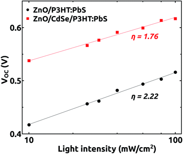 | ||
| Fig. 5 Dependence of VOC on light intensity for the devices grown with and without CdSe buffer layer. | ||
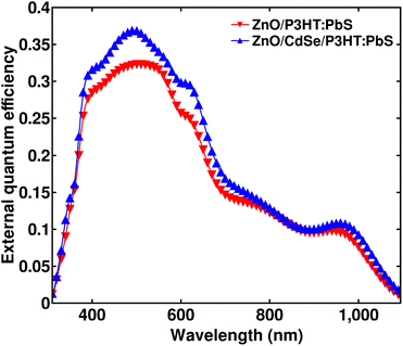
Our arguments on the role of CdSe layer based on the energy band diagram is further supported by the EQE plot shown in Fig. 6. The integrated EQE spectra give a short circuit current density that agrees well with the measured JSC with an error percentage less than 5. We can see an improvement of EQE in almost the entire region of absorption after the CdSe layer is inserted. But the absorptance of the active layer didn't change much in this region by the introduction of the CdSe layer as shown in Fig. S5.† This is suggestive of the fact that the CdSe layer has negligible or no role in the charge generation part. The overall improvement in EQE is therefore attributed to an improvement in the charge collection rather than the charge generation.
Variation of the photovoltaic parameters with respect to the QDs size (Table 1) can be explained as follows. QDs of lower size degrade the mobility35,36 of the buffer layer resulting in an increase of device series resistance, bringing down the cell parameters JSC, FF and PCE. An enhancement of VOC in this case can be attributed to the more closely aligned conduction bands of CdSe and PbS. QDs of higher size can result in an energy level mismatch between ZnO and the CdSe buffer layer due to the reduced band gap of the QDs. This can act as a barrier for the charge carriers in the ZnO/CdSe interface resulting in a reduction of VOC, JSC and the PCE.25
Our result that the PCE decreases with increase of buffer layer thickness is in agreement with the previous reports. Higher thickness of the buffer layer can be result in a weakening of electric field that will reduce the drift velocity, enhancing the carrier recombination in buffer layer.24,25 Hence a reduction in PCE of the devices with increase of buffer layer thickness is caused by the enhanced recombination and the additional series resistance offered by it.
Conclusions
P3HT:PbS bulk-heterojunction inverted hybrid solar cells having the structure ITO/ZnO/CdSe/P3HT:PbS/Au were developed utilizing ZnO as an electron transporting layer and CdSe QDs as the interface buffer layer. The buffer layer promotes electron transport in the device by providing an intermediate energy band relay between ZnO and the active layer. It also reduces the recombination at the ZnO/active layer interface by passivating the ZnO surface states. The enhanced electron transport by the buffer layer reduces the interface carrier density that also helps in decreasing the interface recombination.Conflicts of interest
There are no conflicts to declare.Acknowledgements
The corresponding author V. V. Ison gratefully acknowledges SERB, DST, Govt. of India, for an earlier fast track project (Order No. SR/FTP/PS-108/2010). The authors thank Dr P. R. Biju, Associate Professor, School of Pure and Applied Physics, Mahatma Gandhi University, Kottayam for his support during the solar cell fabrication.References
- X. Lan, O. Voznyy, A. Kiani, F. P. G. deArquer, A. S. Abbas, G.-H. Kim, M. Liu, Z. Yang, G. Walters, J. Xu, M. Yuan, Z. Ning, F. Fan, P. Kanjanaboos, I. Kramer, D. Zhitomirsky, P. Lee, A. Perelgut, S. Hoogland and E. H. Sargent, Adv. Mater., 2016, 28, 299–304 CrossRef CAS PubMed.
- S.-H. Liao, H.-J. Jhuo, P.-N. Yeh, Y.-S. Cheng, Y.-L. Li, Y.-H. Lee, S. Sharma and S.-A. Chen, Sci. Rep., 2014, 4, 6813 CrossRef CAS PubMed.
- H. Zhou, Q. Chen, G. Li, S. Luo, T.-B. Song, H.-S. Duan, Z. Hong, J. You, Y. Liu and Y. Yang, Science, 2014, 345, 542–546 CrossRef CAS PubMed.
- P. Reiss, E. Couderc, J. De Girolamo and A. Pron, Nanoscale, 2011, 3, 446–489 RSC.
- F. Gao, S. Ren and J. Wang, Energy Environ. Sci., 2013, 6, 2020–2040 RSC.
- E. Strein, A. Colbert, S. Subramaniyan, H. Nagaoka, C. W. Schlenker, E. Janke, S. A. Jenekhe and D. S. Ginger, Energy Environ. Sci., 2013, 6, 769–775 RSC.
- N. C. Greenham, X. Peng and A. P. Alivisatos, Phys. Rev. B: Condens. Matter Mater. Phys., 1996, 54, 17628 CrossRef CAS PubMed.
- D. S. Ginger and N. C. Greenham, J. Appl. Phys., 2000, 87, 1361 CrossRef CAS.
- H.-C. Chen, C.-W. Lai, I.-C. Wu, H.-R. Pan, I.-W. P. Chen, Y.-K. Peng, C.-L. Liu, C.-h. Chen and P.-T. Chou, Adv. Mater., 2011, 23, 5451–5455 CrossRef CAS PubMed.
- S. Ren, L.-Y. Chang, S.-K. Lim, J. Zhao, M. Smith, N. Zhao, V. Bulovic, M. Bawendi and S. Gradecak, Nano Lett., 2011, 11, 3998–4002 CrossRef CAS PubMed.
- W. U. Huynh, J. J. Dittmer and A. P. Alivisatos, Science, 2002, 295, 2425–2427 CrossRef CAS PubMed.
- J. J. H. Pijpers, R. Ulbricht, K. J. Tielrooij, A. Osherov, Y. Golan, C. Delerue, G. Allan and M. Bonn, Nat. Phys., 2009, 5, 811–814 Search PubMed.
- J. B. Sambur, T. Novet and B. A. Parkinson, Science, 2010, 330, 63–66 CrossRef CAS PubMed.
- O. E. Semonin, J. M. Luther, S. Choi, H.-Y. Chen, J. Gao, A. J. Nozik and M. C. Beard, Science, 2011, 334, 1530–1533 CrossRef CAS PubMed.
- L. Tan, P. Li, B. Sun, M. Chaker and D. Ma, ChemNanoMat, 2016, 2, 601–615 CrossRef CAS.
- C. Giansante, R. Mastria, G. Lerario, L. Moretti, I. Kriegel, F. Scotognella, G. Lanzani, S. Carallo, M. Esposito, M. Biasiucci, A. Rizzo and G. Gigli, Adv. Funct. Mater., 2015, 25, 111–119 CrossRef CAS.
- C. Borriello, A. Bruno, R. Diana, T. Di Luccio, P. Morvillo, R. Ricciardi, F. Villani and C. Minarini, Phys. Status Solidi A, 2014, 212, 245–251 CrossRef.
- Y. Firdaus, E. Vandenplas, A. Khetubol, D. Cheyns, R. Gehlhaar and M. V. der Auweraer, J. Appl. Phys., 2015, 117, 095503 CrossRef.
- J. Huang, Z. Yinb and Q. Zheng, Energy Environ. Sci., 2011, 4, 3861–3877 RSC.
- Z. Liang, Q. Zhang, L. Jiang and G. Cao, Energy Environ. Sci., 2015, 8, 3442–3476 RSC.
- L. Zhu, B. J. Richardson and Q. Yu, Phys. Chem. Chem. Phys., 2016, 18, 3463–3471 RSC.
- A. P. Litvin, I. D. Skurlov, I. G. Korzhenevskii, A. Dubavik, S. A. Cherevkov, A. V. Sokolova, P. S. Parfenov, D. A. Onishchuk, V. V. Zakharov, E. V. Ushakova, X. Zhang, A. V. Fedorov and A. V. Baranov, J. Phys. Chem. C, 2019, 123, 3115 CrossRef CAS.
- C. Thu, P. Ehrenreich, K. K. Wong, E. Zimmermann, J. Dorman, W. Wang, A. Fakharuddin, M. Putnik, C. Drivas, A. Koutsoubelitis, M. Vasilopoulou, L. C. Palilis, S. Kennou, J. Kalb, T. Pfadler and L. Schmidt-Mende, Sci. Rep., 2018, 8, 3559 CrossRef PubMed.
- M. Yuan, O. Voznyy, D. Zhitomirsky, P. Kanjanaboos and E. H. Sargent, Adv. Mater., 2014, 27, 917–921 CrossRef PubMed.
- T. Zhao, E. D. Goodwin, J. Guo, H. Wang, B. T. Diroll, C. B. Murray and C. R. Kagan, ACS Nano, 2016, 10, 9267–9273 CrossRef CAS PubMed.
- T.-W. Zeng, I.-S. Liu, F.-C. Hsu, K.-T. Huang, H.-C. Liao and W.-F. Su, Opt. Express, 2010, 18, A357–A365 CrossRef CAS PubMed.
- A. Thomas, A. E. Tom, A. D. Rao, K. A. Varman, K. Ranjith, R. Vinayakan, P. C. Ramamurthy and V. V. Ison, J. Appl. Phys., 2014, 115, 104302 CrossRef.
- J. M. Luther, M. Law, Q. Song, C. L. Perkins, M. C. Beard and A. J. Nozik, ACS Nano, 2008, 2, 271–280 CrossRef CAS PubMed.
- S. Pradhan, A. Stavrinadis, S. Gupta and G. Konstantatos, ACS Appl. Mater. Interfaces, 2017, 9, 27390–27395 CrossRef CAS PubMed.
- M. J. Greaney, S. Das, D. H. Webber, S. E. Bradforth and R. L. Brutchey, ACS Nano, 2012, 6, 4222–4230 CrossRef CAS PubMed.
- D. Lee, J. Lim, M. Park, J. Y. Kim, J. Song, J. Kwak, S. Lee, K. Char and C. Lee, Nanotechnology, 2015, 26(46), 465401 CrossRef PubMed.
- K. Lu, Y. Wang, Z. Liu, L. Han, G. Shi, H. Fang, J. Chen, X. Ye, S. Chen, F. Yang, A. G. Shulga, T. Wu, M. Gu, S. Zhou, J. Fan, M. A. Loi and W. Ma, Adv. Mater., 2018, 30, 1707572 CrossRef PubMed.
- Z. Sun, G. Sitbon, T. Pons, A. A. Bakulin and Z. Chen, Sci. Rep., 2015, 5, 10626 CrossRef PubMed.
- M. J. Speirs, D. M. Balazs, H. H. Fang, L. H. Lai, L. Protesescu, M. V. Kovalenko and M. A. Loi, J. Mater. Chem. A, 2015, 3(4), 1450–1457 RSC.
- M. S. Kang, A. Sahu, D. J. Norris and C. D. Frisbie, Nano Lett., 2010, 10, 3727–3732 CrossRef CAS PubMed.
- M. S. Kang, A. Sahu, D. J. Norris and C. D. Frisbie, Nano Lett., 2011, 11, 3887–3892 CrossRef CAS PubMed.
Footnote |
| † Electronic supplementary information (ESI) available. See DOI: 10.1039/d0ra02740e |
| This journal is © The Royal Society of Chemistry 2020 |

