
 Open Access Article
 This Open Access Article is licensed under a Creative Commons Attribution-Non Commercial 3.0 Unported Licence
Synergistic effect of the anti-solvent bath method and improved annealing conditions for high-quality triple cation perovskite thin films†
Geoffrey Ryan Adams ,
Vincent Obiozo Eze,
Lucas Braga Carani,
Aaron Pino,
Claire Jolowsky and
Okenwa I. Okoli*
,
Vincent Obiozo Eze,
Lucas Braga Carani,
Aaron Pino,
Claire Jolowsky and
Okenwa I. Okoli*
High Performance Materials Institute, FAMU-FSU College of Engineering, Tallahassee, FL 32310, USA. E-mail: ookoli@fsu.edu
First published on 12th May 2020
Abstract
One step solution processing together with anti-solvent engineering is a tested route in producing high-quality perovskite films due to its simplicity and low fabrication costs. Commercialization of perovskites will require replacing the anti-solvent drip process and lowering annealing temperatures to decrease the energy payback time. In this work, we successfully replace the anti-solvent drip with the anti-solvent bath (ASB) method through balancing the methylammonium (MA) and formamidinium (FA) cations to produce high-quality cesium (Cs)/FA/MA triple cation perovskite films. Furthermore, the annealing parameters of Cs0.05FA0.16MA0.79PbI2.7Br0.3 are enhanced to allow for a low-temperature fabrication process when paired with the ASB method. This resulted in the formation of remarkable films with micrometer grains and few defects. Self-powered photodetectors were constructed using the improved conditions, resulting in devices that exhibited a low dark current, an on/off ratio of >103, and a rapid rise time of 12.4 μs. The conclusion of this work shows that ASB can be applied to triple cation perovskites and in using this method, the previously established optimal annealing temperature is lowered.
Introduction
Interest in perovskite materials has seen a drastic incline in publications since the successful work of Miyasaka in 2009. This international focus has springboarded advances in fabrication methods for highly crystalline perovskite films for use in solar cells, LEDs, and photodetectors.1–5 Perovskite's attention is much deserved, given the excellent material properties, such as a tuneable band gap,6 high ultraviolet-visible (UV-vis) band absorption,7 and long diffusion lengths8 all available for drastically lower fabrication costs than classical inorganic semiconductors.9,10 However, to achieve high-performance vertical structured devices many factors such as film quality, device architecture, selection of hole transporting layer (HTL) and electron transporting layer (ETL), and additional quenching/passivating layers all play interacting roles.11–14 Due to the interactive nature of each factor, the attributed success of a device's ‘recipe’ can become convoluted, necessitating a narrower scope in future studies. Looking specifically at the factor of ‘film quality’, annealing conditions and precursor chemistry are two intertwined elements that strongly affect the outcome of the perovskite thin films.6,15–17Perovskite is defined by its crystalline structure, ABX3, where classically ‘A’ is the cation, ‘B’ the metal, and ‘X’ the halide site. By splitting the ‘A’ site amongst cesium (Cs), formamidinium (FA), and methylammonium (MA) and the ‘X’ site between iodine (I) and bromine (Br), a ‘triple cation’ perovskite was created by Saliba et al.18 This triple cation perovskite showed to be both high-performing and resistant towards thermal degradation. CsFA, MAFA, and CsMAFA all tout high performance with enhanced thermal stability.18–21 Unfortunately, the presence of FA oftentimes leads to a resultant δ-phase, or ‘yellow’ photo-inactive phase, which is unstable and readily breaks down into the base salt constituents.22,23 However, upon the correct cation balance, the system crystallizes into the ‘black’ photo-active α-phase, which is more resilient towards heat and moisture degradation.18,24
Numerous reports have shown it is difficult to create a high-quality uniform thin film using the single-step method without the use of an anti-solvent before the annealing step.17,18,25–30 Depending on the chemistry of the salts and choice of precursor solvent, anti-solvents such as chlorobenzene, toluene, or dichlorobenzene are dripped onto the spinning device at some improved volume, rate, and time into the programed spin coating step.26,29 These variables lead to a lack of control, repeatability, and scalability due to the fact the drops are dispersed during the spin coating step. In light of these complications, Zhou et al. developed an anti-solvent bath (ASB) method which replaces the anti-solvent drip with the submersion of the dispersed precursor solution and substrate.31 This resulted in high quality, uniform films due to the rapid extraction of the solvent, with the added bonus of an annealing free process for the MAPbI3 chemistry. However, the same group and others rapidly followed-up this work showing that changing the chemistry of the precursor solution results in the change of bonding energy between salts and solvent, leading to a re-optimization of ASB method and even the re-addition of annealing in order to achieve stable, high quality films.32–34
Ideal processing conditions would eliminate the annealing step all together via room temperature crystallization from ASB method. An attempt was made to fabricate room-temperature Cs/FA/MA triple cation films using an anti-solvent drip method, but the results showed lingering PbI2, δ-phase, and intermediate phase due to the lack of annealing.35 This shows that in order to minimize the amount of Cs for preferred crystal orientation,35 annealing is needed to both fully eliminate the cubic PbI2 and photo-inactive δ-phases. Some reports have shown optimization studies for the annealing time and temperature of mixed cation perovskites, but differ in precursor chemistry and do not employ ASB method.36 Furthermore, literature has shown that the optimum annealing temperature for Cs/FA/MA containing triple cation perovskite is 100 °C for varied amounts of time, which results in uniform films showing sub-micron grain size.18,21,37 This shows that the combination of proven triple cation perovskite chemistries in conjunction with ASB method and lower annealing temperatures would pave the way for scalable commercial fabrication such as roll to roll processing on plastics and textiles. Therefore, it is important to investigate the synergistic effects of ASB method and annealing temperature on improving the film quality of triple cation perovskite.
Herein, we investigate the cooperative effect of using anti-solvent bath and improved annealing conditions to prepare high-quality triple cation perovskite films. We elucidated that the ratio of FA to MA plays a critical role in the crystallization of Cs0.05FA0.95−xMAxPbI2.7Br0.3 perovskite thin films when applying the ASB method using diethyl ether. The triple cation perovskite film with the chemical composition of Cs0.05FA0.16MA0.79PbI2.7Br0.3 exhibited the best film quality after annealing at the optimal conditions of 80 °C for 120 min. The resultant perovskite film revealed a drastic increase in grain size and fewer boundaries. In order to further validate the conclusions drawn via the material characterizations of the triple cation thin films, vertical structure photodetectors were constructed and tested.
Results and discussion
First, we varied the FA![[thin space (1/6-em)]](https://www.rsc.org/images/entities/char_2009.gif) :MA ratio to determine the optimal Cs0.05FA0.95−xMAxPbI2.7Br0.3 perovskite chemical composition. The X-ray diffraction (XRD) peaks are shown in Fig. 1 for the FA:MA triple cation thin films annealed at 150 °C, then tested for thermal stability by being further subjected to 85 °C for 2 hours. The annealing temperature and the temperature for the thermal stability studies were selected in accordance with previous reports.38 A full description of the perovskite chemical make-up is given in detail in Table S1 of the ESI.† It can be seen that the FA rich triple cation perovskite was unable to fully transition into the α-phase perovskite, which has been reported to be around 14.36° for the (001) plane.39 Instead the FA rich film (0.79 FA:0.16 MA) crystallized entirely into the photo-inactive δ-phase which resulted in the sharp peak at 11.66°.18 As the FA is replaced with MA, the δ-phase peak is drastically reduced. This reaction shows that the amount of MA was too small to stabilize the FA rich system, likely due to the rapid crystallization from the diethyl ether bath.32 The α-phase peak continually strengthens with the addition of MA, until it reaches its maximum at the FA:MA ratio of 0.28:0.67. It is clear that the MA rich perovskite film is resilient to thermal degradation treatment with an increase in α-phase peak. For further analysis, the full width half maximum (FWHM) is summarized in Table S2 of the ESI.† There is an observed broadening of the FA rich samples' FWHM as the films were aged on the hotplate; however, FWHM decreased for the MA rich samples. This indicates that the MA rich samples benefited from increased time on the hot plate during the attempt at thermal degradation.
:MA ratio to determine the optimal Cs0.05FA0.95−xMAxPbI2.7Br0.3 perovskite chemical composition. The X-ray diffraction (XRD) peaks are shown in Fig. 1 for the FA:MA triple cation thin films annealed at 150 °C, then tested for thermal stability by being further subjected to 85 °C for 2 hours. The annealing temperature and the temperature for the thermal stability studies were selected in accordance with previous reports.38 A full description of the perovskite chemical make-up is given in detail in Table S1 of the ESI.† It can be seen that the FA rich triple cation perovskite was unable to fully transition into the α-phase perovskite, which has been reported to be around 14.36° for the (001) plane.39 Instead the FA rich film (0.79 FA:0.16 MA) crystallized entirely into the photo-inactive δ-phase which resulted in the sharp peak at 11.66°.18 As the FA is replaced with MA, the δ-phase peak is drastically reduced. This reaction shows that the amount of MA was too small to stabilize the FA rich system, likely due to the rapid crystallization from the diethyl ether bath.32 The α-phase peak continually strengthens with the addition of MA, until it reaches its maximum at the FA:MA ratio of 0.28:0.67. It is clear that the MA rich perovskite film is resilient to thermal degradation treatment with an increase in α-phase peak. For further analysis, the full width half maximum (FWHM) is summarized in Table S2 of the ESI.† There is an observed broadening of the FA rich samples' FWHM as the films were aged on the hotplate; however, FWHM decreased for the MA rich samples. This indicates that the MA rich samples benefited from increased time on the hot plate during the attempt at thermal degradation.
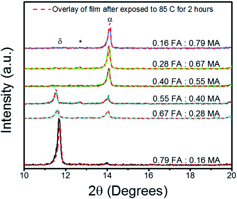 | ||
| Fig. 1 XRD results of Cs0.05FA0.95−xMAxPbI2.7Br0.3 perovskite thin films grown on FTO/c-TiO2 substrates both before and after heat degradation via hotplate at 85 °C for 2 hours in glovebox. Peaks are labelled to denote the δ-phase (δ), cubic PbI2 (*), and α-phase (α). The full length scans can be found in Fig. S1 in the ESI.† | ||
In order to further investigate the Cs0.05FA0.95−xMAxPbI2.7Br0.3 films, scanning electron microscopy (SEM) was performed and is displayed in Fig. S2.† The FA rich films represented the smallest median grain size while the MA rich exhibited the largest median grain size at ∼300 nm (Fig. S3†). The SEM images of the films after ‘degradation’ substantiate the XRD results, as it clearly shows the thermal ‘degradation’ step improves the median grain size for the MA rich samples.
UV-vis was performed on all the samples before and after heating which revealed a decrease in absorption for all cases exhibiting a strong α-phase peak, except the MA rich (0.16 FA:0.79 MA) perovskite (Fig. S4†). This increased absorption after an attempt at thermal degradation can be explained by the increase in grain size seen in the SEM results (Fig. S3†), as the grains would be growing in the x, y, and z directions. These results show a successful application of the ASB method for triple cation films through the balance of FA and MA to eliminate the δ-phase, previously present when ASB was applied.35 Additionally, the combination of XRD, SEM, and UV-vis reveal annealing time and temperature should be further improved for the MA rich solution (0.16 FA:0.79 MA). Therefore, focus was shifted onto only the MA rich solution (0.16 FA:0.79 MA) to study the result of annealing temperature and time optimization.
The MA rich films were fabricated as detailed in the Experimental section, with the exception of annealing time and temperature, which was varied between 80 °C and 150 °C for times of 30, 60, 90, and 120 min. Fig. 2 shows the XRD results for the MA rich solution at the varied annealing times and temperatures, with peaks indexed from literature.39 The previous annealing configuration (150 °C, 30 min) used to produce the films analyzed in Fig. 1 was on the edge of degradation, as the 150 °C films at 60, 90, and 120 min show diminishing perovskite peaks and strong cubic phase PbI2. Although previous reports had concluded that 100 °C was an optimal annealing temperature for triple cation perovskite,18,21,37,40 other literature had shown that 150 °C was necessary for the complete evaporation of the NMP solvent when also employing ASB method.33,41 The FWHM of the (001) peaks from the 80 °C films show stronger crystallinity than the 150 °C films (Table S3†). Thus we conclude that stable α-phase Cs/FA/MA containing triple cation perovskite can be achieved via lower temperatures than previously reported18,21,37,40 when coupled with ASB bath and balancing the FA:MA ratio.
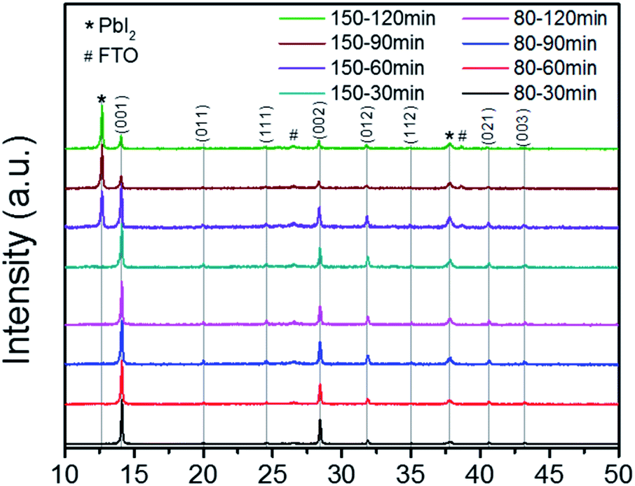 | ||
| Fig. 2 XRD results for 80 °C (bottom four results) and 150 °C (top four results) for the MA rich solution (0.16 FA:0.79 MA). | ||
Fig. 3 shows the UV-vis results as annealing time and temperature are varied, as well as the original MA rich sample from the FA:MA ratio study (Fig. S4†), which served as a control. It can be seen in Fig. 3a that all processing temperatures and times widely mimic the results found for the 150 °C – 30 min setting, with the exception of the 120 min samples. Other than the 30 min case, the absorption for the 150 °C samples are disregarded since they had degraded into cubic PbI2 and remnant α-phase perovskite. The increased absorption of these degraded samples could be due to increased diffraction of light. As the sample degrades, the surface roughness is increased which increases the diffraction of light passing through the sample; mimicking an intensification in absorption.42,43 To further investigate the absorption findings, the film thickness was measured via a profilometer (Fig. S5†). These findings show a slight increase in thickness for the 80 °C films which is indicative of grain growth. However, there is a linear decrease in thickness as a function of annealing time for the 150 °C case. This is in good agreement with the XRD results in Fig. 2 as it indicates the degradation of the crystalline grains and a burn-off of the organic MA and FA material. Fig. 4 shows the SEM results for the MA rich (0.16 FA:0.79 MA) films. It is quickly obvious that the 120 min time period for the 80 °C annealing temperature resulted in the largest grains. This increase in grain size is in good agreement with the increased film thickness and absorption displayed in Fig. S5† and Fig. 3a, respectively. The degradation seen in the XRD results for the 150 °C films is further confirmed through SEM, showing the grain boundaries have dissolved. Large gaps are found across the surface due to the evaporation of the organic cations as the perovskite crystal structure breaks down. Furthermore, increased roughness of the 150 °C for 60, 90, and 120 min samples is evident, indicating increased diffraction seen in Fig. 3b. The mean grain size is calculated for further quantification and available in Table S3.†
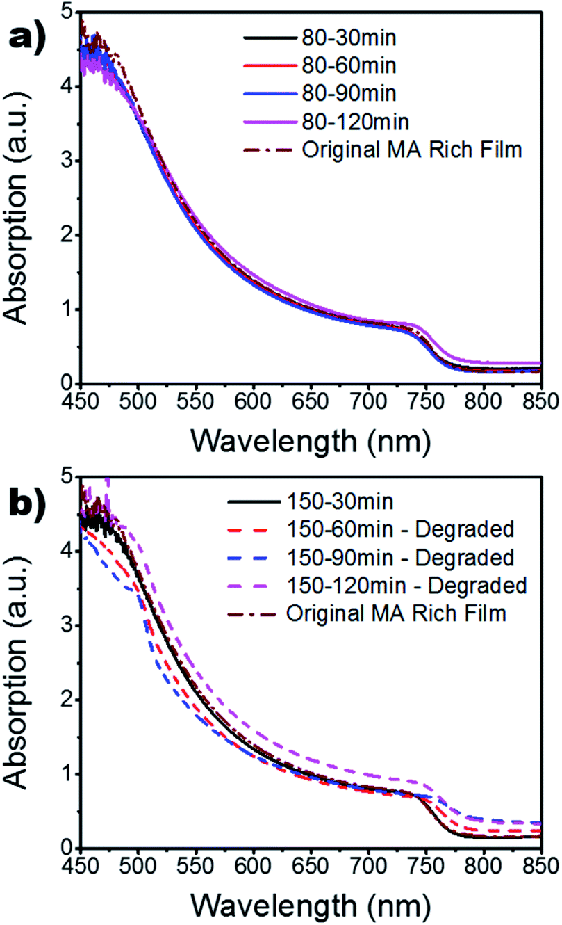 | ||
| Fig. 3 UV-vis of MA rich films for various annealing times at (a) 80 °C and (b) 150 °C. The original MA rich films from the FA vs. MA study are also included for reference. | ||
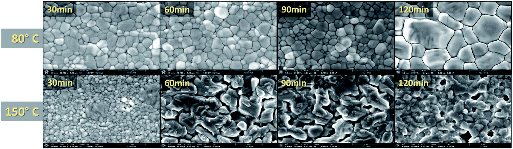 | ||
| Fig. 4 SEM of MA rich films at various annealing times and temperatures (all images taken at ×30000 magnification). | ||
Using the improved annealing parameters of 80 °C and 120 min, self-powered photodetectors were constructed to further characterize the outcome of the large grain films. The development of a more stable self-powered photodetector with rapid response time is of paramount importance for the development of structural health monitoring and in situ damage sensors.44–50 The device followed the p–i–n structure using FTO/compact TiO2 (c-TiO2)/Cs0.05FA0.16MA0.79PbI2.7Br0.3/spiro-OMeTAD/Au as shown in the schematic in Fig. 5a. Typically, the perovskite layer can generate electron–hole pairs that swiftly dissociate at the TiO2/perovskite and perovskite/spiro-OMeTAD interfaces when it absorbs photon energies larger than its bandgap, leading to an efficient architecture for self-powered photodetectors (see Fig. 5b). It is important to note that the proposed use of this photodetector does not necessitate the optimization of the device's fill factor (the sustainment of jsc as a function of voltage), as it will be operating at V = 0. Under self-powered mode (0 V bias), the device showed a low dark current of 2.02 nA cm−2 leading to an on/off ratio of 1.73 × 10³ when exposed to white light with an intensity of 100 mA cm−2. The devices were further tested under monochromatic light conditions using LEDs at 465 nm (blue), 585 nm (yellow), 625 nm (red) while holding the device under a 0 V bias (Fig. 5d). It can be seen that the device's response to the LEDs is agreeable to the UV-vis results which show increased absorption in the higher energy region (see Fig. 3a).
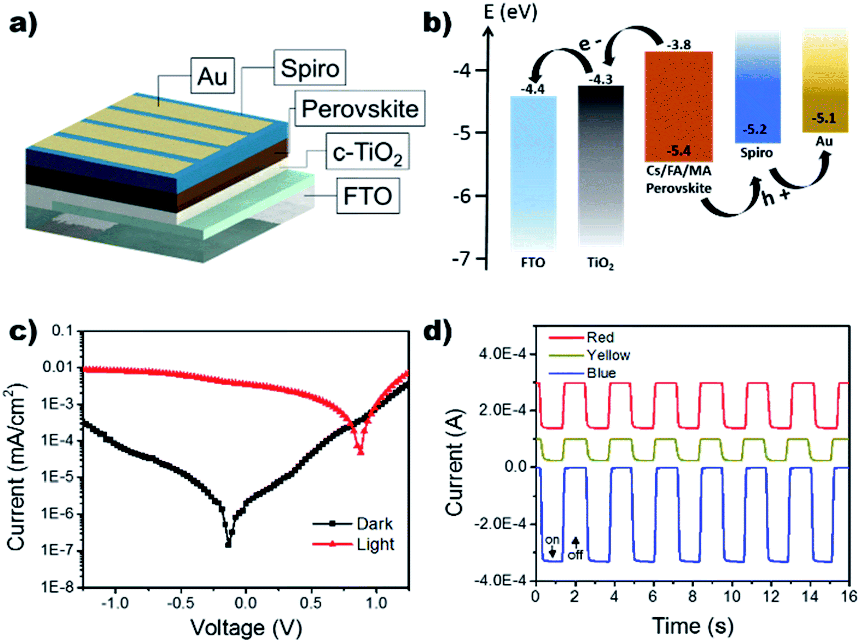 | ||
| Fig. 5 (a) Schematic diagram of the device structure. (b) Energy level diagram (c) J–V curves of the device (using improved fabrication parameters of 80 °C and 120 min) in the dark and under white light illumination (100 mW cm−2). (d) Current vs. time for devices at 0 V bias under various LED illumination (465 nm (48 mW cm−2), 585 nm (24 mW cm−2), 625 nm (24 mW cm2)). | ||
The response time of the device under self-powered mode was measured using a function generator to control the square wave oscillation for the power input to the LED light source. The response was collected using a NI-6210 and signal booster, rendering the output as photovoltage. Fig. 6b shows an extremely rapid rise time of 12.4 μs and a slightly slower decay time of 26.4 μs. A longer decay is not uncommon and has often been attributed to the trapping/detrapping process, governed by interfacial recombination and the selection of HTL.51,52 Therefore, the microsecond response time can be attributed to the device's pristine films and large grain boundaries, decreasing bulk density trap states.
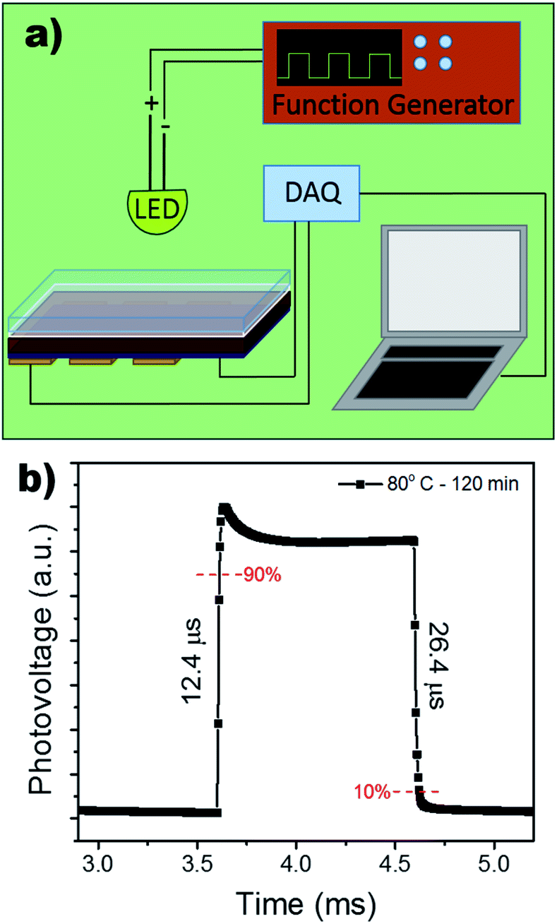 | ||
| Fig. 6 (a) Schematic of experimental set-up for the response time measurement. (b) Response time measurement of photodetector under 0 V bias. | ||
To further investigate the thermal stability of the enhanced perovskite layer, bulk trap density was measured via dark I–V characterization. Electron only devices were fabricated using FTO/TiO2/Cs0.05FA0.16MA0.79PbI2.7Br0.3/PCBM/Au. The trap density of states (DOSt) was calculated using eqn (1), where ε is the relative permittivity of the material, εo is the permittivity of free space, q is the elementary charge, and L is the thickness of the material.
 | (1) |
The thickness of the material was measured via profilometer, outlined in the Experimental section. It has been shown in past reports that the dielectric constant of triple cation perovskite is widely invariant from FAPbI3.53 Therefore, the dielectric value used for the DOS calculation is 46.9.54,55 The ‘pristine’ film in Fig. 7b refers to the device before it began any thermal degradation (t = 0). Although there is a slight decrease (∼0.25 × 1016 cm−3) in mean trap density between t = 0 and t = 5 h, the associated error in the measurement shows no significant variance in the bulk trap density as the films are aged on the hot plate. This suggests there was no degradation of the films over the 5 hour period of exposure, substantiating the thermal stability seen in the XRD results in Fig. S6.† This is a good indication the thermal stability was not altered, although the chemical composition was adapted in order to replace the anti-solvent drip with the ASB method.
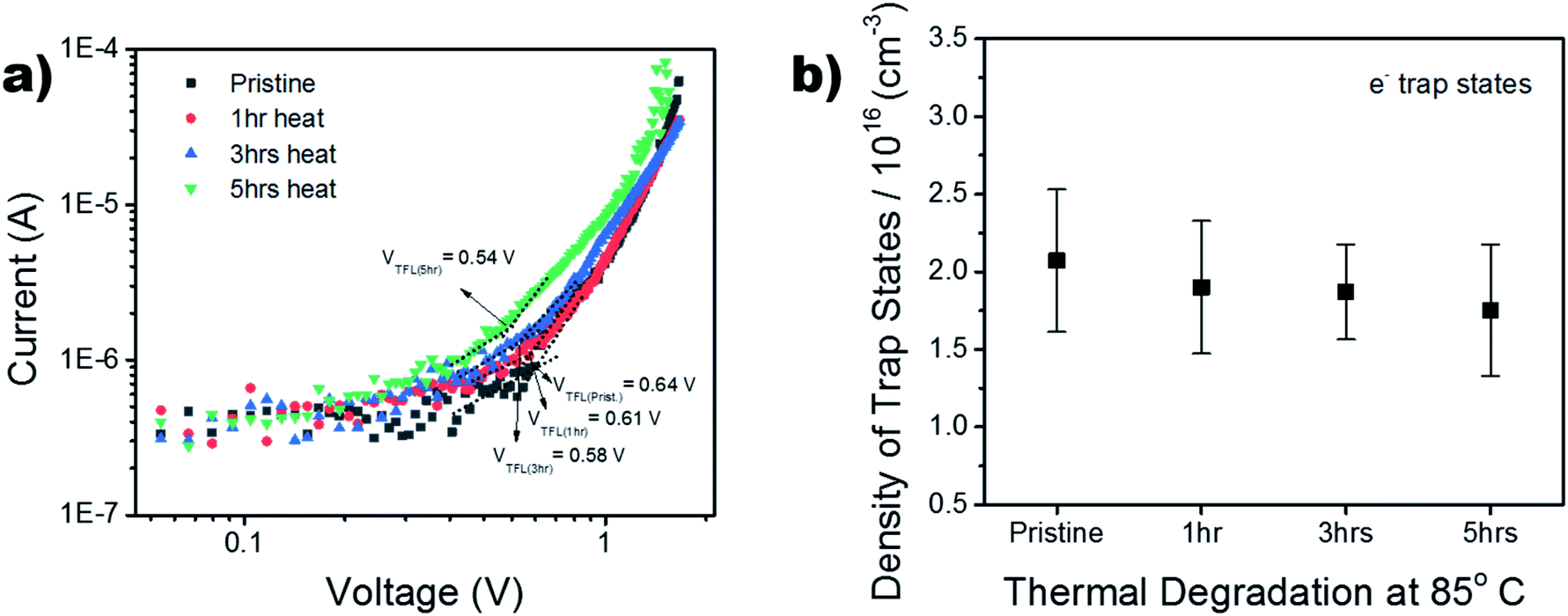 | ||
| Fig. 7 (a) Dark IV measurements of electron only devices. VTFL is calculated for the pristine and thermally degraded samples. (b) Trap density calculations based on the dark IV measurements and identified VTFL. | ||
Conclusion
Perovskite photodetector commercialization has been brought one step closer through the successful application of the scalable ASB method with thermally stable triple cation perovskite. By balancing the amount of FA in the Cs0.05FA0.95−xMAxPbI2.7Br0.3 system, the photo-inactive δ-phase was eliminated for the first time in films produced using the scalable ASB method. Furthermore, it was found that upon applying the ASB method, the annealing temperature could be decreased from 150 °C to 80 °C. Through annealing optimization, >1 μm grains were produced to comprise highly crystalline and uniform thin films. Using the large grained triple cation perovskite, photodetectors were fabricated and characterized. The self-powered device, although employing a simple, non-passivating device architecture (TiO2 and spiro-OMeTAD only), produced a competitively low dark current of 2.02 nA cm−2, on/off ratio of 1.73 × 10³, and rapid rise of 12.4 μs. This study knits together a route for scalable fabrication of highly crystalline, large grain, and thermally stable perovskite films for use in opto-electronic perovskite devices.Experimental
Materials and reagent
Lead bromide (PbBr2, 99%), cesium iodide (CsI, 99%), methylammonium iodide (MAI, 99%), formamidinium iodide (FAI, >98%), 2,2′,7,7′-tetrakis[N,N-di(4-methoxyphenyl)amino]-9,9′-spirobifuorene (spiro-OMETAD, Sigma-Aldrich, 99%), lithium bis(trifluoromethane)sulfonimide (Li-TFSI, 99%), 4-tert-butylpyridine (TBP, 99%), and tris (2-(1H-pyrazol-1-1yl)-4-tert-butylpyridine) cobalt(III) tri[bis(trifluoromethane)sulfonamide] (Co(III) TFSI > 99.95%) were purchased from Sigma-Aldrich. Lead iodide (PbI2, 99.99%) was purchased from Acros. Liquid detergent (Hellmanex) and titanium(IV) chloride (TiCl4) were purchased from Alfa Aesar. Fluorine-doped tin oxide (FTO) glass substrates (sheet resistance: 12–15 Ω per sq.) were purchased from MSE supplies.Thin film preparation and device fabrication
FTO-coated glass substrates were patterned by etching with hydrochloric acid (HCl) and zinc (Zn) powder and sequentially cleaned with Hellmanex, nano pure water, acetone, and isopropanol in a sonication bath for 10 min each. The substrates were then treated with oxygen plasma cleaner for 5 min. The compact TiO2 (c-TiO2) electron transport layer (ETL) was prepared as described in a previous report56 and spin-coated at 3000 rpm for 30 s then immediately dried at 125 °C for 10 min inside a N2 atmosphere. The samples were then removed into ambient conditions and annealed at 500 °C for 30 min (using a rate of 20 °C min−1). The perovskite layer was prepared using a single-step deposition and anti-solvent bath method (described in further detail in a previous report33) back inside the glovebox. The perovskite solutions were prepared inside the glove box. Solutions were made following a ratio of 380 mg:918 mg (cation/halide:metal/halide) in 1 ml of N-methyl-2-pyrrolidone (NMP, Sigma-Aldrich) and 0.2 ml of γ-butyrolactone (GBL, Sigma-Aldrich). The mixed cation solution follows the mass concentration of (Cs0.05FA0.95−xMAx) Pb(I0.9Br0.1)3. The exact values of each solution can be found in the ESI in Table S1.† The solutions were mixed overnight at 70 °C and held at this temperature during deposition. The perovskite layer was deposited through spin coating in a glovebox N2 atmosphere at 4500 rpm for 30 s. Upon completion, the sample was submerged into diethyl ether (Sigma Aldrich) for 2 min, then annealed. The FA vs. MA samples were annealed at 150 °C for 30 min. The Cs0.05FA0.16MA0.79PbI2.7Br0.3 samples were annealed at 80 °C and 150 °C for various times of 30, 60, 90, and 120 min. The hole transporting solution was made using 90 mg of spiro-OMeTAD, 35 μl of 4-tert-butylpyridine, 30 μl of cobalt solution (300 mg of tris(2-(1H-pyrazol-1-yl)-4-tert-butylpyridine)cobalt(III) bis (trifluoromethylsulphonyl) imide in 1 ml of acetonitrile), 18 μl of Li solution (520 mg of bis(trifluoromethane)sulfonimide lithium salt in 1 ml of acetonitrile), and 1 ml of chlorobenzene. For the electron only devices, the PCBM solution was mixed in the glovebox using 20 mg of PCBM in 1 ml of chlorobenzene. The PCBM solution was heated to 60 °C and dispersed via spin coating at 1000 rpm for 30 s, then annealed at 100 °C for 5 min. The devices were masked and placed in the thermal evaporator for gold contact deposition of 100 nm thick at 100 Å s−1. For each device, the active area was defined by a masked area of 0.06 cm2.
Measurement and characterization
The crystalline structure of the as-prepared material was characterized by powder X-ray diffraction (Scintag Pad-V XRD Powder Diffractometer, graphite monochromated Cu Kα radiation). Absorption spectra were collected using Agilent Cary 5000. SEM images were taken by the FEI Helios G4 UC dual field emission electron and Ga ion beam scanning electron microscope. Images were taken with an accelerating voltage of 5 kV. The thickness of the films was measured using the Bruker Dektak XT. The current–voltage (I–V) measurements were obtained by a Keithley 2400 integrated with LabView under a white light LED lamp with intensity of 100 mW cm−2. The photovoltage-response time measurements were obtained using an NI-6210 DAQ. The signal from the DAQ (NI6210) to the computer was boosted with the Hamamatsu C7319 on low bandwidth setting and 105 gain and powered with an Agilent E3630A at 6 V. Matlab was used to collect and process the data. The light source was powered by a GwInstek GFG-8255A function generator, creating a square wave with an amplitude of 2 V to power a 585 nm LED of 37 mW cm−2 intensity.Conflicts of interest
There are no conflicts to declare.Acknowledgements
The authors would like to thank Dr Zhibin Yu for allowing use of the IV testing set-up. We further thank Dr Theo Siegrist and Jennifer Neu for the maintenance and continued access to XRD. The funding for this work was provided by the NSF Award No. 1359235 and NSF/DMR-1644779.References
- N. Wang, L. Cheng, R. Ge, S. Zhang, Y. Miao, W. Zou, C. Yi, Y. Sun, Y. Cao and R. Yang, Nat. Photonics, 2016, 10, 699–704 CrossRef CAS.
- J. Li, S. G. R. Bade, X. Shan and Z. Yu, Adv. Mater., 2015, 27, 5196–5202 CrossRef CAS PubMed.
- M. Ahmadi, T. Wu and B. Hu, Adv. Mater., 2017, 29, 1605242 CrossRef PubMed.
- S. G. R. Bade, J. Li, X. Shan, Y. Ling, Y. Tian, T. Dilbeck, T. Besara, T. Geske, H. Gao and B. Ma, ACS Nano, 2016, 10, 1795–1801 CrossRef CAS PubMed.
- NREL, Best Research-Cell Efficiency Chart, https://www.nrel.gov/pv/cell-efficiency.html Search PubMed.
- L. K. Ono, E. J. Juarez-Perez and Y. Qi, ACS Appl. Mater. Interfaces, 2017, 9, 30197–30246 CrossRef CAS PubMed.
- W. S. Yang, J. H. Noh, N. J. Jeon, Y. C. Kim, S. Ryu, J. Seo and S. I. Seok, Science, 2015, 348, 1234–1237 CrossRef CAS PubMed.
- A. A. Zhumekenov, M. I. Saidaminov, M. A. Haque, E. Alarousu, S. P. Sarmah, B. Murali, I. Dursun, X.-H. Miao, A. L. Abdelhady and T. Wu, ACS Energy Lett., 2016, 1, 32–37 CrossRef CAS.
- M. Cai, Y. Wu, H. Chen, X. Yang, Y. Qiang and L. Han, Adv. Sci., 2017, 4, 1600269 CrossRef PubMed.
- M. Jacoby, Chem. Eng. News, 2016, 94, 30–35 Search PubMed.
- D. B. Khadka, Y. Shirai, M. Yanagida, J. W. Ryan and K. Miyano, J. Mater. Chem. C, 2017, 5, 8819–8827 RSC.
- B. Dänekamp, N. Droseros, D. Tsokkou, V. Brehm, P. P. Boix, M. Sessolo, N. Banerji and H. J. Bolink, J. Mater. Chem. C, 2019, 7, 523–527 RSC.
- U. Krishnan, M. Kaur, M. Kumar and A. Kumar, J. Photonics Energy, 2019, 9, 021001 CAS.
- T. Salim, S. Sun, Y. Abe, A. Krishna, A. C. Grimsdale and Y. M. Lam, J. Mater. Chem. A, 2015, 3, 8943–8969 RSC.
- M. M. Tavakoli, M. Saliba, P. Yadav, P. Holzhey, A. Hagfeldt, S. M. Zakeeruddin and M. Grätzel, Adv. Energy Mater., 2019, 9, 1802646 CrossRef.
- X. Sun, C. Zhang, J. Chang, H. Yang, H. Xi, G. Lu, D. Chen, Z. Lin, X. Lu and J. Zhang, Nano Energy, 2016, 28, 417–425 CrossRef CAS.
- Z. Xiao, Q. Dong, C. Bi, Y. Shao, Y. Yuan and J. Huang, Adv. Mater., 2014, 26, 6503–6509 CrossRef CAS PubMed.
- M. Saliba, T. Matsui, J.-Y. Seo, K. Domanski, J.-P. Correa-Baena, M. K. Nazeeruddin, S. M. Zakeeruddin, W. Tress, A. Abate and A. Hagfeldt, Energy Environ. Sci., 2016, 9, 1989–1997 RSC.
- G. Niu, W. Li, J. Li, X. Liang and L. Wang, RSC Adv., 2017, 7, 17473–17479 RSC.
- Y. Wu, P. Wang, S. Wang, Z. Wang, B. Cai, X. Zheng, Y. Chen, N. Yuan, J. Ding and W. H. Zhang, ChemSusChem, 2018, 11, 837–842 CrossRef CAS PubMed.
- W. Tan, A. R. Bowring, A. C. Meng, M. D. McGehee and P. C. McIntyre, ACS Appl. Mater. Interfaces, 2018, 10, 5485–5491 CrossRef CAS PubMed.
- Y. Fan, H. Meng, L. Wang and S. Pang, Sol. RRL, 2019, 3, 1900215 CrossRef.
- F. Ma, J. Li, W. Li, N. Lin, L. Wang and J. Qiao, Chem. Sci., 2017, 8, 800–805 RSC.
- D. J. Kubicki, D. Prochowicz, A. Hofstetter, P. t. Péchy, S. M. Zakeeruddin, M. Grätzel and L. Emsley, J. Am. Chem. Soc., 2017, 139, 10055–10061 CrossRef CAS PubMed.
- N. J. Jeon, J. H. Noh, Y. C. Kim, W. S. Yang, S. Ryu and S. I. Seok, Nat. Mater., 2014, 13, 897–903 CrossRef CAS PubMed.
- S. Paek, P. Schouwink, E. N. Athanasopoulou, K. Cho, G. Grancini, Y. Lee, Y. Zhang, F. Stellacci, M. K. Nazeeruddin and P. Gao, Chem. Mater., 2017, 29, 3490–3498 CrossRef CAS.
- M. M. Tavakoli, P. Yadav, D. Prochowicz, M. Sponseller, A. Osherov, V. Bulović and J. Kong, Adv. Energy Mater., 2019, 9, 1803587 CrossRef.
- T. T. Ngo, I. Suarez, G. Antonicelli, D. Cortizo-Lacalle, J. P. Martinez-Pastor, A. Mateo-Alonso and I. Mora-Sero, Adv. Mater., 2017, 29, 1604056 CrossRef PubMed.
- M. Konstantakou, D. Perganti, P. Falaras and T. Stergiopoulos, Crystals, 2017, 7, 291 CrossRef.
- C. Wang, C. Zhang, S. Wang, G. Liu, H. Xia, S. Tong, J. He, D. Niu, C. Zhou and K. Ding, Sol. RRL, 2018, 2, 1700209 CrossRef.
- Y. Zhou, M. Yang, W. Wu, A. L. Vasiliev, K. Zhu and N. P. Padture, J. Mater. Chem. A, 2015, 3, 8178–8184 RSC.
- Y. Zhou, M. Yang, O. S. Game, W. Wu, J. Kwun, M. A. Strauss, Y. Yan, J. Huang, K. Zhu and N. P. Padture, ACS Appl. Mater. Interfaces, 2016, 8, 2232–2237 CrossRef CAS PubMed.
- V. O. Eze and T. Mori, Jpn. J. Appl. Phys., 2016, 55, 122301 CrossRef.
- M. Jung, S.-G. Ji, G. Kim and S. I. Seok, Chem. Soc. Rev., 2019, 48, 2011–2038 RSC.
- T. Matsui, J. Y. Seo, M. Saliba, S. M. Zakeeruddin and M. Grätzel, Adv. Mater., 2017, 29, 1606258 CrossRef PubMed.
- H. Yang, J. Zhang, C. Zhang, J. Chang, Z. Lin, D. Chen, H. Xi and Y. Hao, Materials, 2017, 10, 837 CrossRef PubMed.
- T. Hwang, A. J. Yun, J. Kim, D. Cho, S. Kim, S. Hong and B. Park, ACS Appl. Mater. Interfaces, 2019, 11, 6907–6917 CrossRef CAS PubMed.
- M. Saliba, T. Matsui, K. Domanski, J.-Y. Seo, A. Ummadisingu, S. M. Zakeeruddin, J.-P. Correa-Baena, W. R. Tress, A. Abate and A. Hagfeldt, Science, 2016, 354, 206–209 CrossRef CAS PubMed.
- Y. Sun, J. Peng, Y. Chen, Y. Yao and Z. Liang, Sci. Rep., 2017, 7, 1–7 CrossRef PubMed.
- X. Dong, D. Chen, J. Zhou, Y.-Z. Zheng and X. Tao, Nanoscale, 2018, 10, 7218–7227 RSC.
- G. R. Adams, V. O. Eze, M. A. S. Shohag, R. Simpson, H. Parker and O. Okoli, Engineering Research Express, 2020 Search PubMed.
- J. Zhang, G. Zhai, W. Gao, C. Zhang, Z. Shao, F. Mei, J. Zhang, Y. Yang, X. Liu and B. Xu, J. Mater. Chem. A, 2017, 5, 4190–4198 RSC.
- T. Zhang, M. Yang, Y. Zhao and K. Zhu, Nano Lett., 2015, 15, 3959–3963 CrossRef CAS PubMed.
- J. Yan, M. J. Uddin, D. O. Olawale, T. J. Dickens and O. O. Okoli, in Triboluminescence, Springer, 2016, pp. 351–377 Search PubMed.
- M. A. S. Shohag, E. C. Hammel, D. O. Olawale and O. O. Okoli, 2016.
- M. A. S. Shohag, S. A. Tran, T. Ndebele, N. Adhikari and O. I. Okoli, Mater. Des., 2018, 153, 86–93 CrossRef CAS.
- D. O. Olawale, G. Sullivan, T. Dickens, S. Tsalickis, O. I. Okoli, J. O. Sobanjo and B. Wang, Struct. Health Monit., 2012, 11, 139–147 CrossRef.
- M. A. S. Shohag, Z. Jiang, E. C. Hammel, L. Braga Carani, D. O. Olawale, T. J. Dickens, H. Wang and O. I. Okoli, J. Intell. Mater. Syst. Struct., 2018, 29, 883–895 CrossRef.
- M. A. S. Shohag and O. I. Okoli, Composites, Part A, 2019, 116, 114–125 CrossRef CAS.
- M. A. Shohag, T. Ndebele and O. Okoli, Struct. Health Monit., 2019, 18, 1129–1140 CrossRef.
- R. Dong, Y. Fang, J. Chae, J. Dai, Z. Xiao, Q. Dong, Y. Yuan, A. Centrone, X. C. Zeng and J. Huang, Adv. Mater., 2015, 27, 1912–1918 CrossRef CAS PubMed.
- M. Zhang, F. Zhang, Y. Wang, L. Zhu, Y. Hu, Z. Lou, Y. Hou and F. Teng, Sci. Rep., 2018, 8, 1–9 CrossRef PubMed.
- K. Poorkazem and T. L. Kelly, Sustainable Energy Fuels, 2018, 2, 1332–1341 RSC.
- Y. Huang, L. Li, Z. Liu, H. Jiao, Y. He, X. Wang, R. Zhu, D. Wang, J. Sun and Q. Chen, J. Mater. Chem. A, 2017, 5, 8537–8544 RSC.
- Q. Han, S. H. Bae, P. Sun, Y. T. Hsieh, Y. Yang, Y. S. Rim, H. Zhao, Q. Chen, W. Shi and G. Li, Adv. Mater., 2016, 28, 2253–2258 CrossRef CAS PubMed.
- V. O. Eze, B. Lei and T. Mori, Jpn. J. Appl. Phys., 2016, 55, 02BF08 CrossRef.
Footnote |
| † Electronic supplementary information (ESI) available. See DOI: 10.1039/d0ra02719g |
| This journal is © The Royal Society of Chemistry 2020 |