
 Open Access Article
 This Open Access Article is licensed under a
 Creative Commons Attribution 3.0 Unported Licence
Drastic power factor improvement by Te doping of rare earth-free CoSb3-skutterudite thin films†
Cédric Bourgès,
Naoki Sato,
Takahiro Baba,
Tetsuya Baba,
Isao Ohkubo ,
Naohito Tsujii and
Takao Mori*
,
Naohito Tsujii and
Takao Mori*
WPI-MANA, CFSN, National Institute for Materials Science (NIMS), Namiki 1-1, Tsukuba 305-0044, Japan. E-mail: MORI.Takao@nims.go.jp
First published on 3rd June 2020
Abstract
In the present study, we have focused on the elaboration of control of Te-doped CoSb3 thin films by RF magnetron sputtering which is an attractive technique for industrial development of thermoelectric (TE) thin films. We have successfully synthesized sputtering targets with a reliable approach in order to obtain high-quality films with controlled stoichiometry. TE properties were then probed and revealed a reliable n-type behavior characterized by poor electrical transport properties. Tellurium substitution was realized by co-sputtering deposition and allowed obtaining a significant enhancement of the power factor with promising values of PF ≈ 0.21 mW m−1 K−2 near room temperature. It is related to the Te doping effect which leads to an increase of the Seebeck coefficient and the electrical conductivity simultaneously. However, despite this large improvement, the properties remained far from the bulk material and further developments are necessary to improve the carrier mobility reduced by the thin film formatting.
Introduction
Thermoelectricity represents a technological gateway in the current research dynamic focused on sustainable energy development. Through appropriate devices, thermoelectric (TE) materials are attractive for dynamically harvesting energy from surroundings, like body heat, to power Internet of Things (IoT) applications.1,2 For such applications, the development of thermoelectric materials characterized by large TE performance near room temperature is required in addition to preferable flexible formatting. Significant power harvesting from waste heat requires TE material with a high power factor (PF) and low thermal conductivity.3 The TE performance of those materials is quantified by the dimensionless figure of merit zT = PF × Tκ−1 = S2σTκ−1 (T, absolute temperature; S, Seebeck coefficient; σ, electrical conductivity; κ, thermal conductivity). These properties typically have a tradeoff relationships, and several strategies have been investigated, such as various nanostructuring,4,5 utilizing interfaces and composites,6–8 magnetism,9–11 and topological states,12 to bypass these tradeoffs and enhance the zT.For the past more than two decades, skutterudite CoSb3 has been considered as one of the most promising TE material mostly for mid-temperature (300–800 K).13–16 Its high carrier mobility and suitable Seebeck coefficient lead to attractive PF, even near room temperature, and both conduction types (p and n) are achieved. Moreover, its relatively complex cubic structure contained two icosahedra voids formed by the CoSb3 octahedra which allowed the introduction of a foreign element M for acting as a dopant or/and promoting intrinsic low thermal conductivity. Many efforts have been done to obtain further improvement in the electrical transport properties and reduce the lattice thermal conductivity, such as doping and nanostructuring.14,15,17–21 More recently, several studies have reported the thin films synthesis of CoSb3 skutterudite in order to exploit the effects of interface and grain boundary in the low-dimensional system, that can effectively scatter phonons, for promoting low thermal conductivity.22–34 In fact, TE generator based on thin films is attracting much attention for potential IoT applications as sensors, micro-power sources, flexible devices.1,2 Various thermoelectric materials composed of abundant elements have been fabricated into thin films. For example, oxides and some very high performance thin films has been recently reported with Heusler compounds, for example.35–37 Although some promising results have been published regarding CoSb3 skutterudite thin films, the electrical properties remain lower than those of bulk materials due to the difficulty in controlling element composition during preparation.22,29,31,33 Guest ion (rare-earth or alkali-earth metal)-free skutterudites are suitable for thin films growth because they are not easily oxidized.27 Since guest ion plays an important role in lowering thermal conductivity, we need to reduce the high thermal conductivity of guest ion-free skutterudite by other methods.29,30 Substitution of Sb by semimetals elements is a utilized strategy to affect the electronic structure of the CoSb3 skutterudite by increasing the carrier concentration/electrical conductivity, in addition, to reduce the lattice thermal conductivity by phonon-electron scattering enhancement. Up to this date, several studies on Te-doped or Si-doped CoSb3 materials have been made in bulk material and seem effective to enhance the electrical and thermal properties.17,21,38–41 Fabrication of thin films samples based on these materials can be expected to benefit us to obtain further improved rare-earth free skutterudite materials.
In the present study, we were focused on the elaboration of rare earth-free CoSb3−xTex skutterudite thin films by magnetron sputtering which is one of the numerous techniques for preparing thin films at an industrial scale. We have realized CoSb3 target for sputtering with a reliable approach for controlling the raw material parameters. Then CoSb3−xTex thin films were deposited by co-sputtering using CoSb3 and pure Te targets. Different power was used for the Te target in order to obtain different doping levels and optimize the electronic and thermal transport properties simultaneously.
Experimental procedures
Target preparation
For the CoSb3 target, pure elemental Co (powder, ≥99.9%, ≤150 μm, Aldrich) and Sb (powder, ≥99.9%, −100 mesh, Aldrich) were weighed according to the nominal composition of CoSb3. The elemental powders were mixed and ground by hand milling in an agate mortar and sealed in a quartz tube under a dynamic vacuum. The mixture was melted/quenched at 1423 K in an electric furnace and annealed 4 days at 973 K. The obtained powder mixture was sieved through >212 μm and loaded into a graphite die with a diameter of 50 mm coated with carbon paper. Densification by spark plasma sintering (SPS – 511S, Fuji Electronic Industrial) was processed at 773 K for 5 min (heating and cooling rate of 50 K min−1) under a pressure of 40 MPa and vacuum enclosure.For the Te target, a high purity commercial Te target (99.99%, Furuuchi Chemical Company) was used.
Film preparation
CoSb3 skutterudite thin films were prepared by RF co-sputtering deposition technique via AVC-corporation double chamber magnetron sputtering ultrahigh vacuum system. The Pyrex glass was chosen as substrates, which were cleaned by using ultrasonic cleaning for 10 min in acetone, 10 min in absolute ethyl alcohol, and 10 min in deionized water, respectively. The chamber was pumped down to 5.0 × 10⁻⁶ Pa and the working pressure was kept in 1.0 Pa with Ar flow of 6 cm3 min−1. All the samples were deposited with the same sputtering power of 50 W for the CoSb3 target and 0 W, 5 W, 7 W, and 9 W were used for the Te target, respectively, for T1, T2, T3, and T4 film. The sputtering time was set to 3 h at 573 K, then annealing steps of 1 h were taken at the same temperature for preventing the film to peel off. The resulting deposition rates increased with the sputtering power of the Te target and are estimated to be 0.087, 0.088, 0.093, and 0.104 nm s−1 respectively for T1 (0 W), T2 (5 W), T3 (7 W), and T4 (9 W) (S1). Second annealing was realized at 523 K for 1 day under vacuum for crystallizing the skutterudite and improving the films homogeneity. Two substrates were done for each deposition and a second series with a new CoSb3-target was deposited with the same parameters to confirm the results reliability on 4 samples for each condition.Film characterizations
The crystal structure was investigated by X-ray diffraction (XRD) technique with the prescriptive θ–2θ mode with the angle of 2θ = 10°–100° (Smart Lab3 Rigaku Corporation). X-ray powder diffraction patterns were refined by Rietveld analysis using the FullProf and WinPLOTR software packages.42,43 The shape of the diffraction peaks was modeled using a Thompson–Cox–Hastings pseudo-Voigt profile function.44 Zero-point shift, asymmetry parameters and lattice parameters were systematically refined, and the background contribution was manually estimated. The surface morphology was analyzed by scanning electron microscopy (SEM) (Hitachi SU-8000) and the component analysis was proceeded by energy dispersive spectroscopy (EDS). The thickness of the thin films was obtained by using a Dektak 6M Stylus Profiler measurement system. The carrier concentration and mobility were obtained from Hall effect measurements (Resitest 8300). The electrical conductivity (σ) and Seebeck coefficient (S) were simultaneously measured by the four-probe method from 300 K up to 525 K using a ZEM-3 (ULVAK Advance-Riko) device under partial helium pressure. The estimated measurement uncertainties are fixing to 6% for the Seebeck coefficient and 8% for the electrical conductivity.45 The cross-plane thermal conductivity was evaluated by using a picosecond time-domain thermoreflectance (TD-TR) instrument (PicoTR, Picotherm Corp.) in a front-heating/front-detection configuration. A 100 nm-thick Pt thin film was deposited on the CoSb3 film surface by using a DC sputtering system to detect transient temperature changes. A 1550 nm infrared pulsed laser with a repetition frequency of 20 MHz and a pulse duration of 0.5 ps was used as a heat source. A 780 nm probe laser was used to detect the thermoreflectance signal. The picosecond TD-TR system was customized to reduce the spot size of the probe laser to ca. 5 μm as described elsewhere.46 The improved mirror image method for fitting all the range of pulse interval47,48 was used to determine the thermal conductivity value. Here, we assumed the specific heat value of all films as 3R from Dulong–Petit law (0.235 J g−1 K−1).Results and discussion
The X-ray diffraction (XRD) patterns of the whole thin films series after thermal cycles are displayed in Fig. 1a. As can be seen, all patterns exhibited the main diffraction peaks corresponding to the CoSb3 skutterudite structure (Im![[3 with combining macron]](https://www.rsc.org/images/entities/char_0033_0304.gif) , a ≈ 9.04 Å) with high crystallinity as confirmed by cross-section Scanning Electronic Microscope (SEM) (Fig. 2a).49 Additional low-intensity peaks are observable in the sample T1 and can be attributed to residual free-Sb. The main thin films structures were confirmed by XRD refinement considering the CoSb3 skutterudite native structure. Low-reliability factor is obtained independently to the Te target power used during deposition, as presented in Table 1, and confirmed the systematic skutterudite phase formation with high purity. XRD pattern refinement allowed to determine the lattice parameter dependency with the Te target power and permitted to estimate the Te doping level in each film (Table 1 and Fig. 1b). Nonetheless, no conclusion about the atomic distribution of the Te in the Sb site and/or the void site can be drawn from the XRD refinement due to the limited resolution of a conventional XRD diffractometer. The increase in the cell parameter led us to the assumption that Sb substitution by Te occurred in accordance with the previous report on bulk but it is not excluded that the Te partially filled the void position in skutterudite.38,40 Further analysis, using transmission electronic microscope (TEM), is required to elucidate the real position of Te. The pseudo-linear and large increase of the lattice parameter versus Te target power is observable for T3 and T4 in contrast to T2. According to the paper of Li et al., the cell parameter dependence with Te doping level reaches a step at a = 9.053 Å corresponding to a Te substitution of 3.13 at%.38 Nevertheless, in the report of Nagamoto et al., a solubility limit of 6.2 at% is proposed with corresponding cell parameters of a ≈ 9.049 Å.17 In our present study, the cell parameters drastically increased up to a = 9.110 Å for T4 suggesting that a higher doping level can be reached by the sputtering method. The composition analysis by Scanning Electron Microscopy using Energy Dispersive X-ray Spectroscopy (SEM-EDS) also sustained this hypothesis with a richest Te composition (>6.2 at%) for the sample T3 and T4 (Tables 2 and S2†). It revealed a clear tendency of increasing Te content with the increasing of the Te target power simultaneously with a decreasing of the Sb content following the main substitution between the Sb and the Te. Also, as can be seen from Table 2, the thickness of the samples increased slightly in good agreement with the theoretical larger deposition rate, provided by the increasing power of Te target, during co-deposition. Although the EDS analysis showed a Te concentration of 12.22% and 22.14% for T3 and T4 films, respectively, these are likely to include contributions from Sb2Te3 nano particles, as will be shown below. Nevertheless, the large lattice parameters of these samples indicate that the Te concentrations in the CoSb3 phase of sample T3 and T4 are much higher than the solubility limit so far reported for bulk samples.17
, a ≈ 9.04 Å) with high crystallinity as confirmed by cross-section Scanning Electronic Microscope (SEM) (Fig. 2a).49 Additional low-intensity peaks are observable in the sample T1 and can be attributed to residual free-Sb. The main thin films structures were confirmed by XRD refinement considering the CoSb3 skutterudite native structure. Low-reliability factor is obtained independently to the Te target power used during deposition, as presented in Table 1, and confirmed the systematic skutterudite phase formation with high purity. XRD pattern refinement allowed to determine the lattice parameter dependency with the Te target power and permitted to estimate the Te doping level in each film (Table 1 and Fig. 1b). Nonetheless, no conclusion about the atomic distribution of the Te in the Sb site and/or the void site can be drawn from the XRD refinement due to the limited resolution of a conventional XRD diffractometer. The increase in the cell parameter led us to the assumption that Sb substitution by Te occurred in accordance with the previous report on bulk but it is not excluded that the Te partially filled the void position in skutterudite.38,40 Further analysis, using transmission electronic microscope (TEM), is required to elucidate the real position of Te. The pseudo-linear and large increase of the lattice parameter versus Te target power is observable for T3 and T4 in contrast to T2. According to the paper of Li et al., the cell parameter dependence with Te doping level reaches a step at a = 9.053 Å corresponding to a Te substitution of 3.13 at%.38 Nevertheless, in the report of Nagamoto et al., a solubility limit of 6.2 at% is proposed with corresponding cell parameters of a ≈ 9.049 Å.17 In our present study, the cell parameters drastically increased up to a = 9.110 Å for T4 suggesting that a higher doping level can be reached by the sputtering method. The composition analysis by Scanning Electron Microscopy using Energy Dispersive X-ray Spectroscopy (SEM-EDS) also sustained this hypothesis with a richest Te composition (>6.2 at%) for the sample T3 and T4 (Tables 2 and S2†). It revealed a clear tendency of increasing Te content with the increasing of the Te target power simultaneously with a decreasing of the Sb content following the main substitution between the Sb and the Te. Also, as can be seen from Table 2, the thickness of the samples increased slightly in good agreement with the theoretical larger deposition rate, provided by the increasing power of Te target, during co-deposition. Although the EDS analysis showed a Te concentration of 12.22% and 22.14% for T3 and T4 films, respectively, these are likely to include contributions from Sb2Te3 nano particles, as will be shown below. Nevertheless, the large lattice parameters of these samples indicate that the Te concentrations in the CoSb3 phase of sample T3 and T4 are much higher than the solubility limit so far reported for bulk samples.17
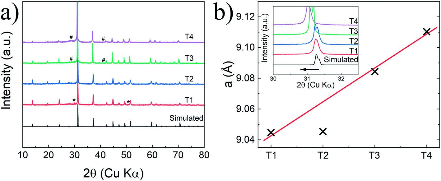 | ||
| Fig. 1 (a) XRD patterns recorded at room temperature of the CoSb3 doped Te thin films (T1, T2, T3, and T4) and the simulated CoSb3 pattern. The (*) attest to the presence of free-Sb reflexion and (#) to the low-intensity peak (015) and (110) of the Sb2Te3 nanoparticles, and (b) evolution of the lattice parameter a and the highlight of the (310) reflexion shift (inset) with the Te target power (the red line is just a guide to the eye). | ||
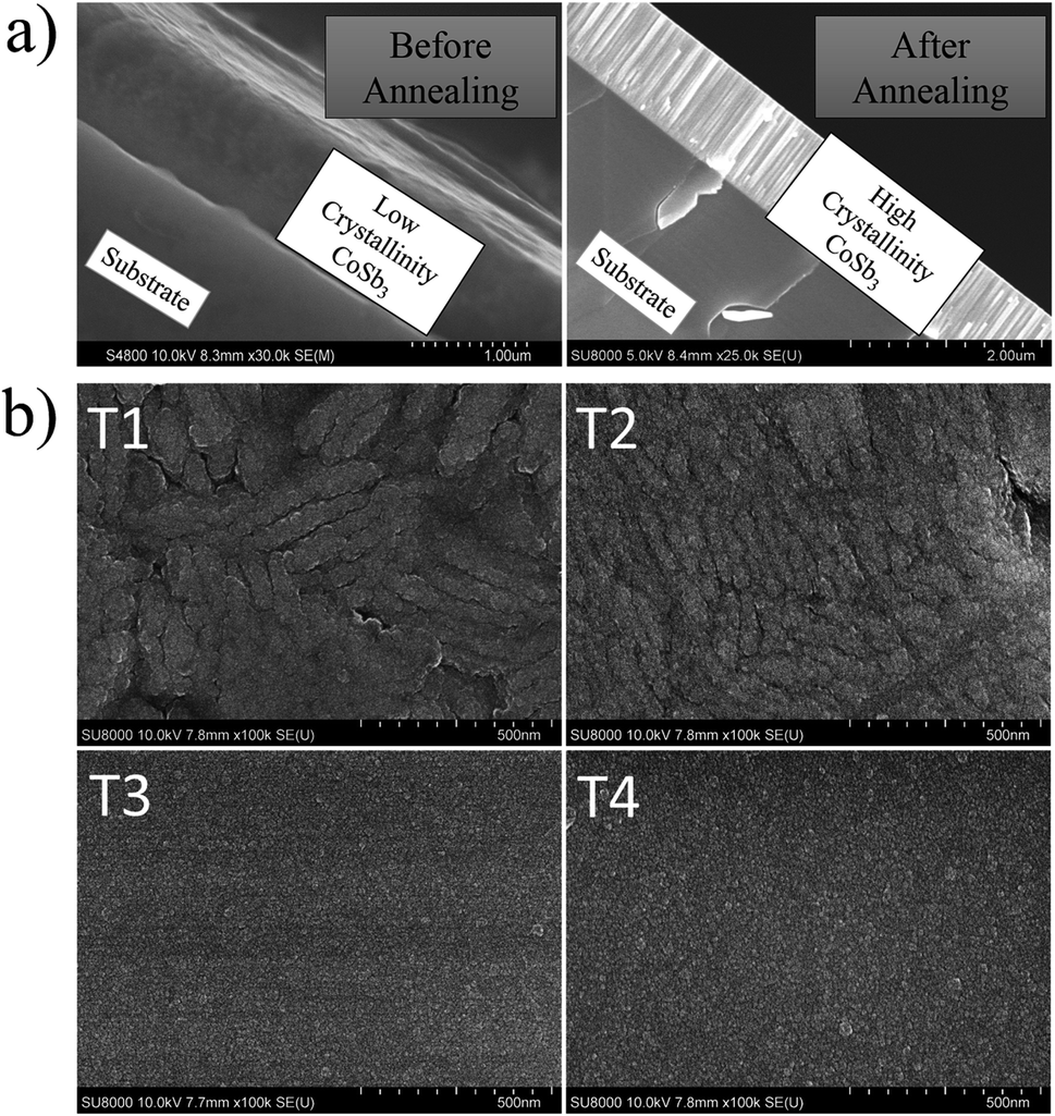 | ||
| Fig. 2 (a) Cross-section SEM image of the undoped CoSb3 thin film before and after annealing and (b) surface morphology of the CoSb3 doped Te thin films (T1, T2, T3, and T4). | ||
| Im |
a (Å) | V (Å3) | χ2 | RF | RBragg |
|---|---|---|---|---|---|
| T1 | 9.0446 | 739.894 | 1.12 | 7.88 | 8.83 |
| T2 | 9.0453 | 740.063 | 1.22 | 5.63 | 8.27 |
| T3 | 9.0844 | 749.690 | 3.22 | 7.52 | 21.9 |
| T4 | 9.1104 | 756.146 | 2.05 | 9.33 | 18.1 |
| Co content (at%) | Sb content (at%) | Te content (at%) | Thickness (nm) | |
|---|---|---|---|---|
| T1 | 19.89 | 80.11 | — | 940 |
| T2 | 20.29 | 76.47 | 3.24 | 951 |
| T3 | 18.20 | 69.58 | 12.22 | 1002 |
| T4 | 15.82 | 62.04 | 22.14 | 1123 |
The substantial Te content affected the surface morphology as shown in Fig. 2. The undoped (T1) and low Te-doped (T2) films revealed a slightly rough surface composed of irregular particles in the range of 100 nm to 1 μm. These particles are assimilated to the crystallized CoSb3-skutterudite as highlighted by the broad diffraction peak (Fig. 1b inset). Nonetheless, the T3 and T4 films revealed a flatter surface covered by nanoscale particles. We ascribed these nanoparticles to a Sb2Te3 phase (RmH, a ≈ 4.26 Å and c ≈ 30.46 Å) which was seeded between the larger CoSb3 particles during the deposition process. This assumption is supported by the XRD pattern of the T4 which exhibited low intensity and broad peaks located at 2θ ≈ 28.20° and 42.40° (Fig. 1a (#)). It can be assimilated to the highest intensity indexation (015) and (110) of the Sb2Te3 crystal structure. Moreover, the Sb–Te rich composition revealed by SEM-EDS analysis (Tables 2 and S2†) also supports this assumption. A recent study has shown that the RF-magnetron sputtering method is suitable for obtaining nanosize Sb2Te3 in the range of 5.8–19.6 nm depending on the annealing.50 The seeding of the Sb2Te3 phase is made propitious by the systematic free-Sb, as observed in the un-doped film T1, and associated with the oversupply of Te provided by the large target power used for T3 and T4 deposition.
All thin films are characterized by n-type conduction with large carrier concentrations in the range of 1021 cm−3 as presented in Fig. 3. It indicates that the deposition process affected the film composition and promoted an intrinsic electron doping effect. According to the study of Zheng et al., the presence of free-Sb in the undoped film T1 (Fig. 1a (*)) attested that an Sb deficiency involved in the CoSb3 film, which thereby induces additional electron carrier leading to the n-type conduction. As an example, the study of P. Fan et al. reported for CoSb3 thin film sample annealed at 518 K a carrier concentration of n ≈ 0.8 × 1021 cm−3 and an electronic mobility of μ ≈ 0.75 cm2 V−1 s−1 at RT (Fig. 3 (*)).31 But in the present study, it can be seen that the undoped film T1 is characterized by slightly larger carrier concentration (n = 2.45 × 1021 cm−3 at RT) and a significantly reduced electronic mobility (μ = 0.14 cm2 V−1 s−1). It suggests that our films are characterized by larger Sb deficiency. By using the data reported by P. Fan et al. as reference values, we can see that the carrier concentration significantly increases with the theoretical Te content up to n = 7.35 × 1021 cm−3 at RT for T4 according to the electron donor effect of the Te substitution.38,39 It is followed by a slight drop of the carrier mobility from μ = 0.463 cm2 V−1 s−1 to 0.362 cm2 V−1 s−1, respectively, for T2 and T4 (Fig. 3). The decrease of the electron mobility can likely to be related to the ionized impurity scattering effect enhancement related to the rise of the carrier concentration between the two samples. Other possibilities can be the alloy scattering and the potential fluctuation effect due to a non-uniform distribution of Te atoms over the lattice.
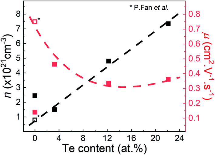 | ||
| Fig. 3 Carrier concentration and electron mobility at room temperature as a function of Te content of the CoSb3 doped Te thin films (T1, T2, T3, and T4) and reference data of CoSb3 thin film annealed at 518 K (asterisk).31 | ||
The electronic mobilities remained low, by comparison with the bulk CoSb3 skutterudite, and drastically affected the electrical transport properties as presented in Fig. 4a. The undoped film T1 exhibited semiconducting behavior with low electrical conductivity σ far from the native properties of the CoSb3 bulk sample.13,14,18,21 This electrical transport behavior is typical for a heavily doped semiconductor. Therefore, it is consistent with the large carrier concentration and the reduced electronic mobility due to the thin film formatting effect and small grain size in all films.33,34 The Te doping effect allowed to improve the electrical conductivity in the whole temperature range by the increase of the carrier concentration. As can be seen in Fig. 4a, electrical conductivity gradually increased with Te content from σ = 4.9 × 10³ S m−1 to 3.5 × 10⁴ S m−1 at 300 K, respectively, for T1 and T4. The presence of nanosize Sb2Te3, in T3 and T4 films, is assumed to have a negligible effect on the electrical properties considering the small amount detected and the poor electrical mobility of this phase.50
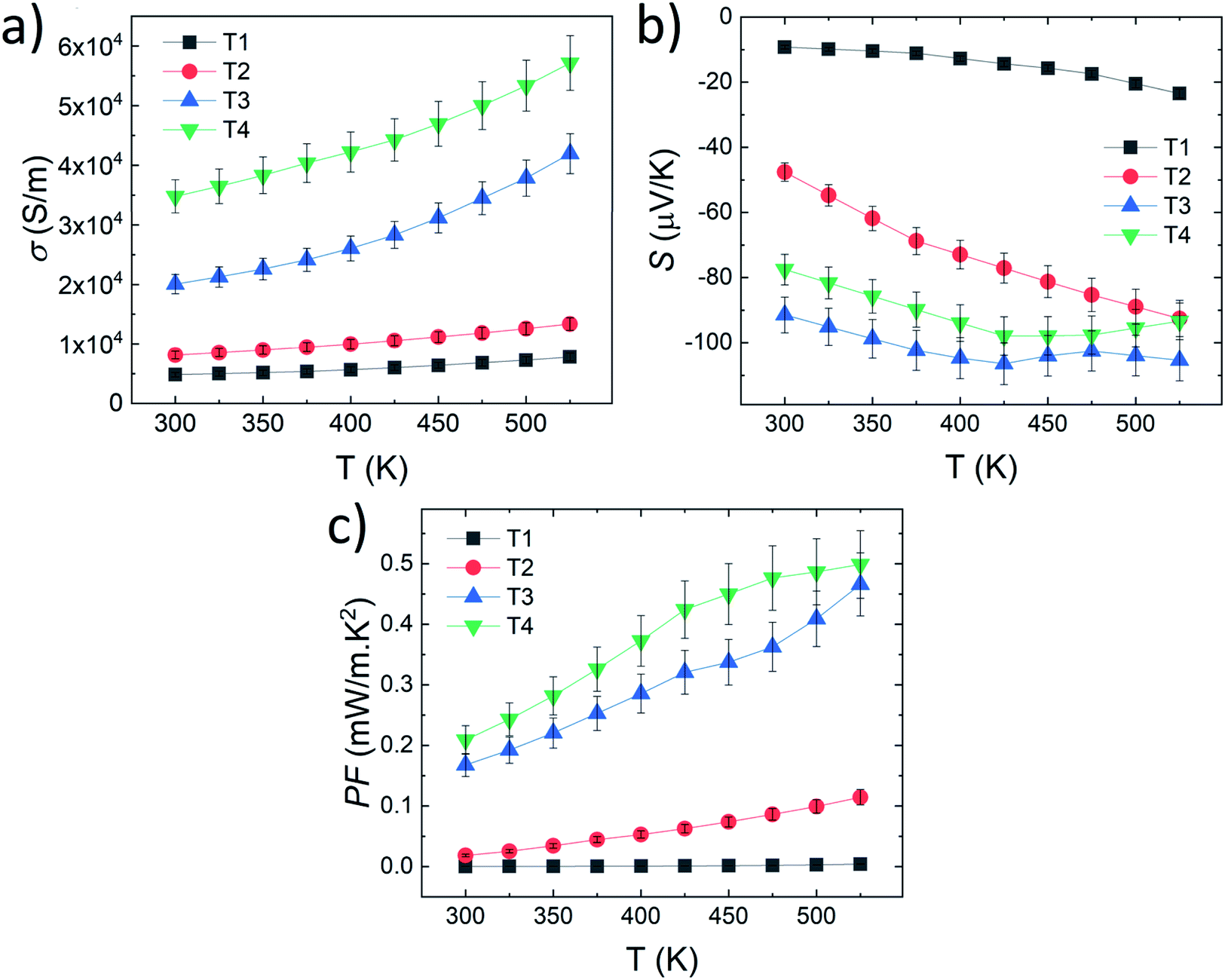 | ||
| Fig. 4 (a) Electrical conductivity σ, (b) Seebeck coefficient S and (c) power factor PF as the function of the temperature of the CoSb3 doped Te thin films (T1, T2, T3, and T4). | ||
The Seebeck coefficient measurement confirmed that the whole series is characterized by n-type conduction with a negative Seebeck coefficient. The undoped film T1 is represented by low values in the temperature range (S = −9.2 to −23.5 μV K−1 from 300 to 525 K; Fig. 4b) comparable with several reports on undoped CoSb3 thin films.31,33,34 However, the Te doping induced a significant increase of the absolute value of the Seebeck coefficient up to S = −91.5 μV K−1 at 300 K for example in T3. The larger carrier concentration of T1 (n = 2.45 × 1021 cm−3 at RT) compared to T2 (n = 1.50 × 1021 cm−3 at RT) follow the predictive Pisarenko plot of the CoSb3-skutterudite presented in the report of Tang et al.51 Indeed, it is consistent with the multiple band transport model proposed for the heavily doped n-type CoSb3 skutterudite and explains the larger absolute Seebeck coefficient of the low Te-doped film T2 compared to the undoped film T1. However, it suggests an additional feature leading to the large thermopower in T3 and T4. As presented before, the large Te amount leads to a change of the crystal structure. The lattice parameter values are significantly increased for the films T3 and T4 (a ≥ 9.0844 Å at 300 K, Table 1) by comparison with T1 and T2 (a ≤ 9.0453 Å). The large Te amount can be considered to have induced a crystal field modification by the variation of the Sb–Co–Sb angle and bond length, as described in the report of Hanus et al.52 The ‘lattice effect’ can contribute to a band convergence in the CoSb3 electronic structure and be cumulated with carrier density effect for promoting a large Seebeck coefficient.
Correlated with the conductivity improvement, the Seebeck enhancement leads to a significant improvement of the PF of the thin film by 2 orders of magnitude in T4 up to a value of PF = 0.21 mW m−1 K−2 at 300 K (PF = 0.50 mW m−1 K−2 at 525 K) as presented in Fig. 4c. To the best of our knowledge, this is the highest power factor obtained in rare earth-free CoSb3-skutterudite thin films near room temperature and represent an improvement of at least 260% compared to the report of Fan et al. on flexible substrates and 840% considering the recent report on Ag-doped CoSb3 skutterudite thin film at room temperature.24,31 The drastic PF improvement, induced by the Te doping effect, constitutes a new record considering the last few years trend of the highest PF obtained on the rare earth-free CoSb3-skutterudite thin films at room temperature (Fig. 5).
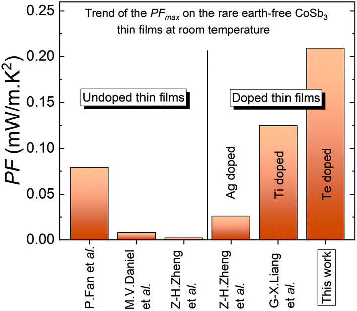 | ||
| Fig. 5 The trend of the highest PF obtained on the rare earth-free CoSb3-skutterudite thin films at room temperature.24,26,30,32,34 | ||
To probe the thin films formatting effect in the thermal transport performance near room temperature, the thermal conductivity of the thin films was measured by the thermoreflectance method with front detection (S3),47,48 using a customized focused system.46,53,54 The results of the calculated total κ and lattice κlatt thermal conductivity are summarized in Table 3. The electronic thermal conductivity κelec contribution seems negligible compared to the lattice thermal conductivity contribution. The pristine sample (T1) presented a significantly reduced κlatt of 3.8 W m−1 K−1 @ 300 K compared to the corresponding values reported on undoped bulk samples (κbulk ≈ 8–9 W m−1 K−1 @ 300 K).38,55–57 According to the theoretical prediction of Shiga et al., a significant κ reduction of CoSb3 thin film should occur for thin films thickness bellow 500 nm.58 However, the present thin films are in the region over 800 nm (Table 2) which confirmed that even ‘thick’ film formatting can efficiently reduce the thermal transport in the CoSb3 phase by the enhancement of boundary scattering in the surface. This effect can be cumulated with the small grain size (<500 nm) and a higher fraction of grain boundaries (Fig. 2b) which can contribute to lower the thermal conductivity as reported in nanostructured CoSb3.59,60 Te doping provided an additional reduction of the κlatt, as already reported in bulk materials. Considering that the samples have a high carrier concentration and low mobility, which indicates a high effective mass, we speculate that phonon-electron scattering can be induced by Te doping and also might have a non-negligible role.21,38 Ultimately we have obtained a minimum value of κlatt = 2.2 W m−1 K−1 @ 300 K for T3. The slightly increased value of κlatt = 2.9 W m−1 K−1 @ 300 K for the T4 film with heavy Te doping might be due to the Sb2Te3 phase which affected the front detection of the thermoreflectance analysis by increasing the interfacial thermal resistance. The final figure of merit varied between zT = 0.02–0.04 near room temperature (300–375 K) and increased up to zT = 0.08–0.1 at 525 K for the T3 and T4 thin films.
| At 300 K | Thermal diffusivity (m2 s−1) | Density (kg m−2) | Specific heat (J (kg−1 K−1)) | Thermal conductivity (W (m−1 K−1)) | Lattice thermal conductivity (W (m−1 K−1)) |
|---|---|---|---|---|---|
| T1 | 2.59 × 10⁻⁶ | 7616 | 235.0 | 3.8 | 3.78 |
| T2 | 1.53 × 10⁻⁶ | 7614 | 235.0 | 3.2 | 3.15 |
| T3 | 1.50 × 10⁻⁶ | 7516 | 235.0 | 2.4 | 2.23 |
| T4 | 2.14 × 10⁻⁶ | 7452 | 235.0 | 3.2 | 2.94 |
Conclusion
In this study, Te-doped CoSb3-skutterudite thin films were prepared for the first time by using the co-sputtering of a CoSb3 target and pure Te target. Tellurium doping was confirmed through XRD refinement and SEM-EDS analysis. We revealed that the sputtering method allowed to overcome the Te solubility limit reported of 6.2 at% on bulk samples. The electron doping provided with the substitution of Sb by Te leads to an increase in the carrier concentration and enhanced the poor electrical conductivity of the CoSb3 thin films up to σ ≈ 3.50 × 10⁴ S m−1 at 300 K for the richest Te content. Simultaneously, the Seebeck coefficient is increased up to S = −93.4 μV K−1 at 525 K for this heavily Te-doped thin films which provided the best power factor currently reported in rare earth-free CoSb3 skutterudite films of PF = 0.21 to 0.50 mW m−1 K−2, respectively, at 300 K and 525 K. Furthermore, we determined the thermal conductivity of the CoSb3-skutterudite thin films (κ = 3.8 W m−1 K−1 @ 300 K for the undoped film) which highlighted that even thick film formatting can efficiently reduce the large thermal conductivity of the phase. Finally, we showed that the co-deposition method is suitable for preparing highly doped-CoSb3 thin films.Conflicts of interest
The authors declare no conflict of interest.Acknowledgements
This paper is based on results obtained from a project commissioned by the New Energy and Industrial Technology Development Organization (NEDO). We also acknowledge support from JST CREST JPMJCR19Q4, Mirai JPMJMI19A1, and JSPS JP16H06441. The authors would like to thank Namiki foundry (NIMS, Japan) for the use of a DC sputtering machine for deposition of Pt layers for the thermoreflectance measurements, and SEM analysis.References
- T. Mori and S. Priya, MRS Bull., 2018, 43, 176–180 CrossRef.
- I. Petsagkourakis, K. Tybrandt, X. Crispin, I. Ohkubo, N. Satoh and T. Mori, Sci. Technol. Adv. Mater., 2018, 19, 836–862 CrossRef CAS PubMed.
- L. E. Bell, Science, 2008, 321, 1457–1461 CrossRef CAS PubMed.
- T. Mori, Small, 2017, 13, 1702013 CrossRef PubMed.
- Z. Liu, J. Mao, T.-H. Liu, G. Chen and Z. Ren, MRS Bull., 2018, 43, 181–186 CrossRef.
- T. Mori and T. Hara, Scr. Mater., 2016, 111, 44–48 CrossRef CAS.
- A. Pakdel, Q. Guo, V. Nicolosi and T. Mori, J. Mater. Chem. A, 2018, 6, 21341–21349 RSC.
- X. Zianni, J. Appl. Phys., 2019, 126, 194301 CrossRef.
- J. B. Vaney, S. Aminorroaya Yamini, H. Takaki, K. Kobayashi, N. Kobayashi and T. Mori, Mater. Today Phys., 2019, 9, 100090 CrossRef.
- N. Tsujii, A. Nishide, J. Hayakawa and T. Mori, Sci. Adv., 2019, 5, eaat5935 CrossRef CAS PubMed.
- T. P. Bailey, R. Lu, P. F. P. Poudeu and C. Uher, Mater. Today Phys., 2019, 11, 100155 CrossRef.
- J. Gooth, G. Schierning, C. Felser and K. Nielsch, MRS Bull., 2018, 43, 187–192 CrossRef CAS.
- T. Caillat, A. Borshchevsky and J. P. Fleurial, J. Appl. Phys., 1996, 80, 4442–4449 CrossRef CAS.
- D. T. Morelli, G. P. Meisner, B. Chen, S. Hu and C. Uher, Phys. Rev. B: Condens. Matter Mater. Phys., 1997, 56, 7376–7383 CrossRef CAS.
- Y. Tang, R. Hanus, S.-W. Chen and G. J. Snyder, Nat. Commun., 2015, 6, 1–7 CAS.
- F. Gucci, T. G. Saunders and M. J. Reece, Scr. Mater., 2018, 157, 58–61 CrossRef CAS.
- Y. Nagamoto, K. Tanaka and T. Koyanagi, in Proceeding of the 17th International Conference on Thermoelectrics, 1998, pp. 302–305 Search PubMed.
- M. K. Choi, S. C. Ur, J. C. Kwon, K. W. Cho, I. H. Kim, Y. G. Lee and S. L. Ryu, Mater. Sci. Forum, 2005, 486–487, 642–645 CAS.
- Q. Jie, H. Wang, W. Liu, H. Wang, G. Chen and Z. Ren, Phys. Chem. Chem. Phys., 2013, 15, 6809–6816 RSC.
- B. R. Ortiz, C. M. Crawford, R. W. McKinney, P. A. Parilla and E. S. Toberer, J. Mater. Chem. A, 2016, 4, 8444–8450 RSC.
- A. U. Khan, K. Kobayashi, D. M. Tang, Y. Yamauchi, K. Hasegawa, M. Mitome, Y. Xue, B. Jiang, K. Tsuchiya, D. Golberg, Y. Bando and T. Mori, Nano Energy, 2017, 31, 152–159 CrossRef CAS.
- J. C. Caylor, A. M. Stacy, R. Gronsky and T. Sands, J. Appl. Phys., 2001, 89, 3508–3513 CrossRef CAS.
- V. Savchuk, A. Boulouz, S. Chakraborty, J. Schumann and H. Vinzelberg, J. Appl. Phys., 2002, 92, 5319–5326 CrossRef CAS.
- Z. H. Zheng, M. Wei, J. T. Luo, F. Li, G. X. Liang, Y. Liang, J. Hao, H. L. Ma, X. H. Zhang and P. Fan, Inorg. Chem. Front., 2018, 5, 1409–1414 RSC.
- A. Masarrat, A. Bhogra, R. Meena, M. Bala, R. Singh, V. Barwal, C.-L. Dong, C.-L. Chen, T. Som, A. Kumar, A. Niazi and K. Asokan, RSC Adv., 2019, 9, 36113–36122 RSC.
- G.-X. Liang, Z.-H. Zheng, F. Li, J.-T. Luo, H. Jin, X.-H. Zhang and P. Fan, J. Eur. Ceram. Soc., 2019, 39, 4842–4849 CrossRef CAS.
- S. R. Sarath Kumar, D. Cha and H. N. Alshareef, J. Appl. Phys., 2011, 110, 083710 CrossRef.
- C. He, M. Daniel, M. Grossmann, O. Ristow, D. Brick, M. Schubert, M. Albrecht and T. Dekorsy, Phys. Rev. B: Condens. Matter Mater. Phys., 2014, 89, 174303 CrossRef.
- Z.-H. Zheng, P. Fan, Y. Zhang, J.-T. Luo, Y. Huang and G.-X. Liang, J. Alloys Compd., 2015, 639, 74–78 CrossRef CAS.
- G. Fu, L. Zuo, J. Chen, M. Lu and L. Yu, J. Appl. Phys., 2015, 117, 125304 CrossRef.
- P. Fan, Y. Zhang, Z.-H. Zheng, W.-F. Fan, J.-T. Luo, G.-X. Liang and D.-P. Zhang, J. Electron. Mater., 2015, 44, 630–635 CrossRef CAS.
- M. V. Daniel, M. Lindorf and M. Albrecht, J. Appl. Phys., 2016, 120, 125306 CrossRef.
- Z.-H. Zheng, M. Wei, F. Li, J.-T. Luo, H.-L. Ma, G.-X. Liang, X.-H. Zhang and P. Fan, J. Mater. Sci.: Mater. Electron., 2017, 28, 17221–17226 CrossRef CAS.
- Z. Zheng, M. Wei, F. Li, J. Luo, G. Liang, H. Ma, X. Zhang and P. Fan, Coatings, 2017, 7, 205 CrossRef.
- P. Mele, S. Saini, H. Honda, K. Matsumoto, K. Miyazaki, H. Hagino and A. Ichinose, Appl. Phys. Lett., 2013, 102, 253903 CrossRef.
- Y. Hirose, M. Tsuchii, K. Shigematsu, Y. Kakefuda, T. Mori and T. Hasegawa, Appl. Phys. Lett., 2019, 114, 193903 CrossRef.
- B. Hinterleitner, I. Knapp, M. Poneder, Y. Shi, H. Müller, G. Eguchi, C. Eisenmenger-Sittner, M. Stöger-Pollach, Y. Kakefuda, N. Kawamoto, Q. Guo, T. Baba, T. Mori, S. Ullah, X. Q. Chen and E. Bauer, Nature, 2019, 576, 85–90 CrossRef CAS PubMed.
- X. Y. Li, L. D. Chen, J. F. Fan, W. B. Zhang, T. Kawahara and T. Hirai, J. Appl. Phys., 2005, 98, 083702 CrossRef.
- K. Kobayashi, A. U. Khan and T. Mori, Jpn. J. Appl. Phys., 2017, 56, 2017 Search PubMed.
- T. Liang, X. Su, Y. Yan, G. Zheng, X. She, Y. You, C. Uher, M. G. Kanatzidis and X. Tang, NPG Asia Mater., 2017, 9, e352 CrossRef CAS.
- W.-S. Liu, B.-P. Zhang, L.-D. Zhao and J.-F. Li, Chem. Mater., 2008, 20, 7526–7531 CrossRef CAS.
- J. Rodríguez-Carvajal, Phys. B, 1993, 192, 55–69 CrossRef.
- T. Roisnel and J. Rodríguez-Carvajal, Mater. Sci. Forum, 2001, 378–381, 118–123 CAS.
- P. Thompson, D. E. Cox and J. B. Hastings, J. Appl. Crystallogr., 1987, 20, 79–83 CrossRef CAS.
- E. Alleno, D. Bérardan, C. Byl, C. Candolfi, R. Daou, R. Decourt, E. Guilmeau, S. Hébert, J. Hejtmanek, B. Lenoir, P. Masschelein, V. Ohorodnichuk, M. Pollet, S. Populoh, D. Ravot, O. Rouleau and M. Soulier, Rev. Sci. Instrum., 2015, 86, 0–9 CrossRef CAS PubMed.
- Y. Kakefuda, K. Yubuta, T. Shishido, A. Yoshikawa, S. Okada, H. Ogino, N. Kawamoto, T. Baba and T. Mori, APL Mater., 2017, 5, 126103 CrossRef.
- T. Baba, Jpn. J. Appl. Phys., 2009, 48, 05EB04 Search PubMed.
- T. Baba, N. Taketoshi and T. Yagi, Jpn. J. Appl. Phys., 2011, 50, 11RA01 CrossRef.
- T. Schmidt, G. Kliche and H. D. Lutz, Acta Crystallogr., 1987, 43, 1678–1679 Search PubMed.
- S. Morikawa, T. Inamoto and M. Takashiri, Nanotechnology, 2018, 29, 075701 CrossRef PubMed.
- Y. Tang, Z. M. Gibbs, L. A. Agapito, G. Li, H.-S. Kim, M. B. Nardelli, S. Curtarolo and G. J. Snyder, Nat. Mater., 2015, 14, 1223–1228 CrossRef CAS PubMed.
- R. Hanus, X. Guo, Y. Tang, G. Li, G. J. Snyder and W. G. Zeier, Chem. Mater., 2017, 29, 1156–1164 CrossRef CAS.
- M. Piotrowski, M. Franco, V. Sousa, J. Rodrigues, F. L. Deepak, Y. Kakefuda, N. Kawamoto, T. Baba, B. Owens-Baird, P. Alpuim, K. Kovnir, T. Mori and Y. V. Kolen'Ko, J. Phys. Chem. C, 2018, 122, 27127–27134 CrossRef CAS.
- F. Pawula, R. Daou, S. Hébert, O. Lebedev, A. Maignan, A. Subedi, Y. Kakefuda, N. Kawamoto, T. Baba and T. Mori, Phys. Rev. B, 2019, 99, 1–7 CrossRef.
- D. T. Morelli, T. Caillat, J. P. Fleurial, A. Borshchevsky, J. Vandersande, B. Chen and C. Uher, Phys. Rev. B: Condens. Matter Mater. Phys., 1995, 51, 9622–9628 CrossRef CAS PubMed.
- J. X. Zhang, Q. M. Lu, K. G. Liu, L. Zhang and M. L. Zhou, Mater. Lett., 2004, 58, 1981–1984 CrossRef CAS.
- M. Rull-Bravo, A. Moure, J. F. Fernández and M. Martín-González, RSC Adv., 2015, 5, 41653–41667 RSC.
- T. Shiga, D. Aketo, L. Feng and J. Shiomi, Appl. Phys. Lett., 2016, 108, 201903 CrossRef.
- M. S. Toprak, C. Stiewe, D. Platzek, S. Williams, L. Bertini, E. Müller, C. Gatti, Y. Zhang, M. Rowe and M. Muhammed, Adv. Funct. Mater., 2004, 14, 1189–1196 CrossRef CAS.
- J. L. Mi, T. J. Zhu, X. B. Zhao and J. Ma, J. Appl. Phys., 2007, 101, 054314 CrossRef.
Footnote |
| † Electronic supplementary information (ESI) available. See DOI: 10.1039/d0ra02699a |
| This journal is © The Royal Society of Chemistry 2020 |