
 Open Access Article
 This Open Access Article is licensed under a Creative Commons Attribution-Non Commercial 3.0 Unported Licence
Ultrasonication assisted fabrication of a tungsten sulfide/tungstite heterostructure for ppb-level ammonia detection at room temperature†
Ravindra Kumar Jha ab,
Aman Nandaa and
Navakanta Bhat*a
ab,
Aman Nandaa and
Navakanta Bhat*a
aCentre for Nano Science and Engineering, Indian Institute of Science, Bangalore, India. E-mail: navakant@iisc.ac.in
bNano-Bio Sensors Group, CSIR-Central Electronics Engineering Research Institute, Pilani, Rajasthan, India-333031
First published on 9th June 2020
Abstract
A heterostructure of WS2/WO3·H2O has been prepared by partial oxidation of WS2 nanosheets by exposing bulk WS2 micron powder to ultrasonic waves in a bath sonicator. The as-prepared nanomaterial was used as a sensing film in an interdigitated electrode-based gas detecting device. The device was found to be specific towards ammonia gas among a group oxidizing and reducing gases. In particular, a response of as high as 11.36–254.66% was recorded for ammonia concentrations of 50 ppb to 2 ppm with excellent repeatability and reproducibility at room temperature. The response time and recovery time of the device was found to be a few tens of seconds suggesting its practicability. A plausible mechanism based on different active sites present in the receptor film is proposed and a logical reason behind its specificity towards ammonia gas is also inferred based on the Lewis acidic centers on the nano-surfaces. Overall, this proposed nanomaterial has very high potential for practical use as a room temperature ammonia sensor.
1. Introduction
Detection of ammonia gas at low concentrations is very important for quality life as this is the most abundant air pollution element contributed by industry, vehicles, and food practices. Apart from this, there are several places in industry processes, breath analysis and other clinical diagnosis where it is necessary to ascertain ammonia concentration with highest possible accuracy.1–3 Several nanomaterials including metal oxides, semiconducting polymers, carbon nanotubes etc. are well established gas sensing receptors films for chemiresistive device applications. With the rise in two-dimensional (2D) material research, several exciting graphene analogous nanomaterials have emerged as an alternative to these existing materials. These materials provide excellent surface-to-volume ratio because of the weak interlayer van-der Waals attraction which allow exfoliation of ultrathin layers with nearly all the atoms exposed to the toxic analyte molecules. This weak interlayer physical forces in these materials (i.e. transition metal dichalcogenides (TMDs), hexagonal boron nitride (h-BN) etc.) allow easy fabrication of vertical heterostructure of 2D materials by simply stacking one over other by physical or chemical techniques as the epitaxial constraints are relaxed for these materials.4 However, the relative orientation control of layers with respect to each other is an important aspect to be considered for vertical heterostructure. The vertically stacked heterogeneous nanomaterials provides a unique opportunity to tune the surface properties via work function tuning. For example, the work function of graphene sheets can be tuned by stacking them on any TMD nanosheets.5 By this stacking, a dipole moment is created across the two planes due to the interlayer charge transfer which could be used for fine control of the chemical reactivity on the surface. The neat interfaces at the heterojunction provide much reliable device performance. Unfortunately, fabrication of lateral heterostructure (with two materials linked by covalent bonding) remains challenging as the lateral growth requires lateral lattice matching. However, Ling et al. demonstrated a modified chemical vapor deposition (CVD) technique to grow lateral heterostructure (or parallel stitching) of 2D materials with even large lattice mismatch.6 In this technique, they sowed aromatic molecules on the substrate as seed to facilitate growth of the two different layers parallelly. A similar approach has also been reported by Zhang et al. to fabricate lateral heterostructure of TMDs.7 Zhou et al. synthesized 2D lateral heterostructure of tungsten sulfide (WS2)/tungstite (WO3·H2O) by supercritical carbon dioxide (sc-CO2) assisted exfoliation of WS2 and then partially converting them into tungsten oxide monohydrate (WO3·H2O) through oxidation of these sheets under high pressure.32In this work, we have synthesized WO3·H2O lateral heterostructure by simply bath sonicating the bulk WS2 micron powder dispersed in ethanol–water (EtOH) and allowed local heating by avoiding any ice addition to the bath. This heating allowed partial oxidation of nanosheets with some water molecule being trapped in the crystal resulting in lattice H2O. Several material characterization tools including XRD, Raman, UV/Vis, SEM, TEM, AFM etc. were utilized to characterize the phase, morphology, and heterogeneous nature of this nanomaterial. This material was further utilized in sensing toxic gases. The device showed excellent selectivity towards ammonia gas at room temperature.
2. Experimental section
2.1. Materials synthesis and characterization
The bulk WS2 micron powder (>99.9% pure (Sigma Aldrich)) was used as the precursor material. Pure ethanol was obtained from Merck while deionized (DI) water of resistivity 18.2 MΩ cm was obtained from a Millipore system. This bulk WS2 micro-powder was dispersed in 40 ml EtOH (ethanol: 65% water: 35% v/v) with an initial concentration of 6 mg ml−1. The solution was ultrasonicated in a low power bath sonicator (PC analytics average power = 120 watt and frequency = 50 kHz) similar to our previous report, except that no ice was added to the bath.8 In place of ice addition, the sonicator was switched off for 1 minute after running for every 15 minutes to save the instrument from overheating. This cycle was repeated for about 72 hours. The dispersion was allowed to settle down for next 24 hours following which, it was centrifuged at 2000 rpm and top one-third of solution was collected for further characterization and device fabrication.The morphology of bulk WS2 and as-obtained nanomaterial was characterized using field-emission scanning electron microscopy (FE-SEM, ULTRA 55, Carl Zeiss AG). Low magnification and high-resolution transmission electron microscope (Low-Mag. TEM, and HR-TEM), high-angle annular dark-field scanning transmission electron microscopy (HAADF-STEM) and corresponding energy dispersive spectroscopy (EDS) mapping analyses were done using a FEI transmission electron microscope (Titan Themis 300 kV) with sample dropcasted on a copper (300 mesh) grid. A Bruker (Dimension Icon) atomic force microscope (AFM) operating in tapping mode was utilized to understand the thickness profile of the nanomaterial. X-ray diffraction (XRD, Rigaku SmartLab) pattern was used to compare the bulk and as-fabricated nanomaterial crystal structure. Raman data was collected using Horiba (LabRAM HR) high-resolution Raman spectrometer equipped with 532 nm laser. Shimadzu UV-3600 UV-VIS-NIR spectrophotometer was employed to collect ultraviolet-visible (UV/Vis) spectrum.
2.2. Fabrication of gas sensor and their sensing measurements
The interdigitated electrode (IDE) with 5 μm width and gap was fabricated by standard photolithography technique as reported in our previous report.9 In brief, 90 nm of platinum (Pt) was deposited over 10 nm titanium (Ti) for IDE fingers and contact pads. 2.5 micro-liter (μL) of the as-prepared nanomaterial was dropcasted manually on the IDE's active area and used as sensing device after drying at 100 °C for half-an-hour in ambient without any post-processing step. This device was probed inside a custom-built gas sensing set-up as reported earlier.10 Commercial synthetic air (standard composition: N2 = 79%, and O2 = 21% by volume) was used to dilute analytes to obtain required concentration. It was also used to attain baseline of the device. A biasing voltage of 1 V was provided to the device during sensing measurements.3. Results and discussion
3.1. WS2/WO3·H2O synthesis
Bulk WS2 powder (as shown in Fig. 1(a)) dispersed in EtOH was subjected to ultrasonic waves for long term (∼72 hours). It should be noted that the bulk WS2 was not able to disperse in pure water and thus, ethanol–water mixture was used as a convenient mixed solvent strategy.11 Generally, to fabricate nanosheets of WS2 (or any other TMDs) this method is taken into consideration and is called liquid phase exfoliation (LPE) as discussed in literature in detail.12–14 However, these experiments are performed in ice-cooling condition to avoid any oxidation which could take place due to local heat generation by strong ultrasonic waves.9,15 In this experiment, the bath sonicator chamber was not cooled (neither ice was added, nor any chiller was connected) and the intentional heat generation due to continuous bubble formation and collapsing due to ultrasonication was allowed. After long hours of sonication, the sample was allowed to settle down for 24 hours before collecting the supernatant of centrifuged sample. The FESEM image of the supernatant nanomaterial is shown in Fig. 1(b). It is evident that tiny nanoflakes have formed by the processing, which is also confirmed by low-mag. TEM images in Fig. 1(c). However, it also shows that many nanoflakes are oriented in vertical direction. It should be noted that we have done a thorough TEM measurements at various places and similar vertically oriented flakes were present along with the flat nanoflakes. This may be due to presence of different nanostructures with distinct surface energy in the liquid processed samples which require specific relaxation energy. The SAED pattern (inset of Fig. 1(c)) also confirmed the polycrystallinity in the sample. The HR-TEM image (as shown in Fig. 1(d)) of the sample clearly shows the heterogeneousness of the sample. The marked area 1 clearly shows the presence of lattice fringes due to (100) and (002) planes of WS2 along with (111) plane of WO3·H2O. Area 2 also reveals these co-existing phases in the sample, along with some defects which may have been resulted from the long hours of sonication. However, both the areas clearly reveal lattice merging and a good interface at the lateral heterojunction. This neat interface is formed due to partial in situ oxidation of WS2 nanosheets which has exfoliated during the sonication.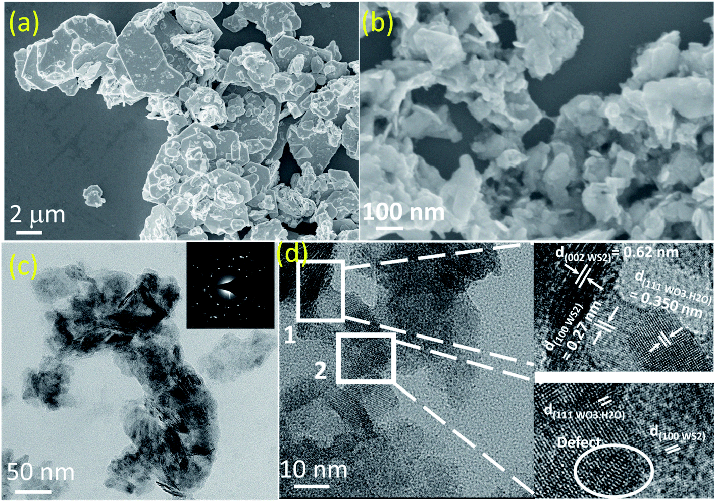 | ||
| Fig. 1 FESEM image of (a) bulk WS2 and (b) as-obtained nanomaterial after ultrasonication for 72 hours and centrifugation at 2000 rpm for 30 minutes; (c) low-mag. TEM image of the as-obtained nanomaterial (inset: SAED pattern) (d) HR-TEM image of the as obtained nanomaterial and zoomed image for two different area from this figure. | ||
We further characterized the nanomaterial via different diffraction and spectroscopy techniques. The XRD pattern of bulk WS2 powder and as-obtained nanomaterial is shown in Fig. 2(a). XRD peak corresponding to (002) peak for the bulk WS2 sample (JCPDS card no. 08-0237) appears at a two-theta (2θ) value of 14.36° which shifts by 0.06° after nanostructuring towards higher 2θ values and appears at 14.42° in the as-obtained nanomaterial.
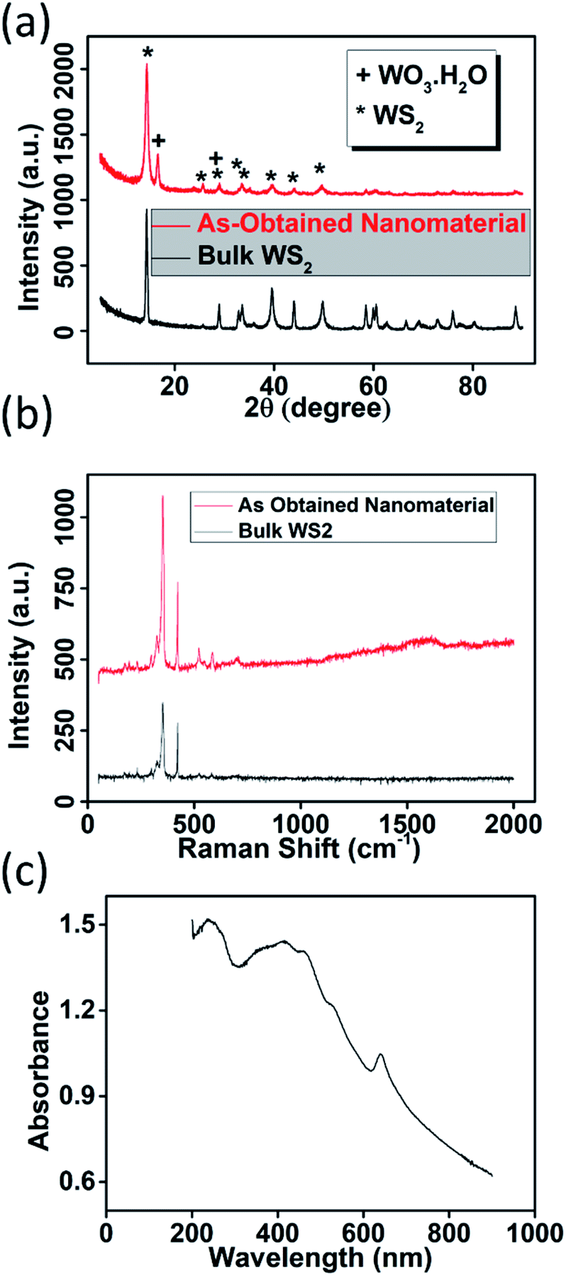 | ||
| Fig. 2 (a) XRD pattern of bulk WS2 and as-obtained nanomaterial (b) Raman spectroscopy data for bulk and as-obtained nanomaterial (c) UV/Vis spectra of as-obtained nanomaterial. | ||
This is unusual in exfoliation as the nanostructuring usually results in shifting to lower 2θ value due to enhanced interplanar crystal spacing.16–18 Therefore, this shift is attributed to the planar tensile stress caused by the partial oxidation of nanosheets.19 Major peak corresponding to WO3·H2O appeared at 16.6° which is 0.1° offset (towards higher 2θ) value from the standard WO3·H2O XRD data (JCPDS card no. 43-0679) again confirming the overall tensile stress in the nanomaterial.20 The Raman data for the exfoliated nanomaterial is compared with the bulk WS2 in Fig. 2(b).
The A1g (out-of plane vibration) peak and E12g (in-plane vibration) peak of WS2 still dominate in the exfoliated nanomaterial, confirming the partial oxidation of the nanosheets. The position of E12g peak in bulk WS2 appears at 352.71 cm−1 which remain intact in the exfoliated sample, however, A1g peak in exfoliated nanomaterial appears to be blue shifted by 0.46 cm−1 as compared to bulk sample. In the higher wavenumber regime, broad hump appears in the Raman signature of the as-obtained nanomaterial which is again due to partial oxidation of the WS2 nanosheets during ultrasonication.21 The UV/Vis data for the exfoliated nanomaterial is shown in Fig. 2(c). The peaks at 239 nm and 406 nm correspond to the two unoccupied anti-bonding components of WO3·H2O, while peaks at 639 nm, 525 nm, and 459 nm correspond to characteristic excitonic A, B, and C band of WS2.22,23 HAADF-STEM image of the nanomaterial is shown in Fig. 3(a) with corresponding elemental mapping of elements in Fig. 3(b–d). These images clearly reveal the presence of oxygen in abundance in the sample. EDAX analysis of the corresponding area (Fig. 3(e) and (f)) clearly indicates the oxygen richness in sample due to partial oxidation. The AFM height profile (Fig. 3(g) and (h)) analysis of the samples showed ultrathin nature of the nanomaterial with thickness in the range of 1–4 nm and lateral dimension in the range 100–200 nm. The corresponding phase data of the AFM image shows nanomaterials with black spot in the center with light yellowish shade at the outer part. This indicates that the WS2 nanosheets are partially oxidized from edges towards center as depicted in schematic diagram in Fig. 4.
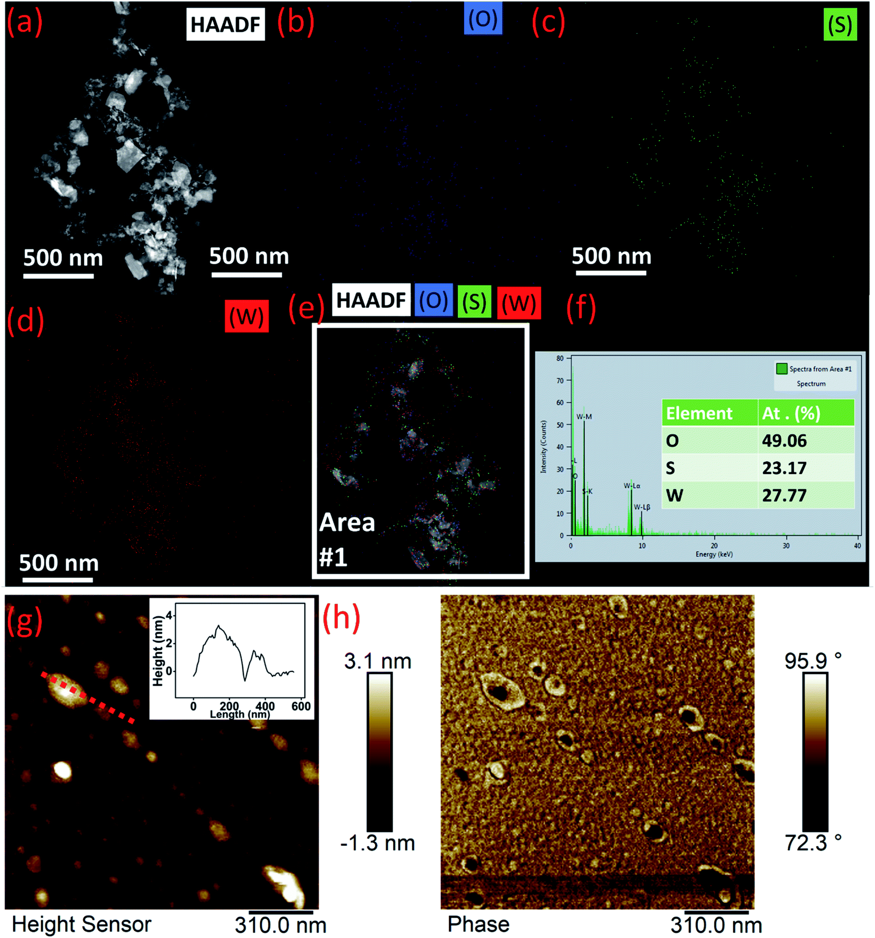 | ||
| Fig. 3 (a) HAADF image of as-synthesized nanomaterial, elemental mapping in the sample corresponding to (b) oxygen (O), (c) sulfur (S), (d) tungsten (W), (e) elemental mapping imposed on HAADF image and (f) corresponding EDAX data (g) AFM image and its height-profile (inset) corresponding to a nanostructure and corresponding (h) AFM phase data. | ||
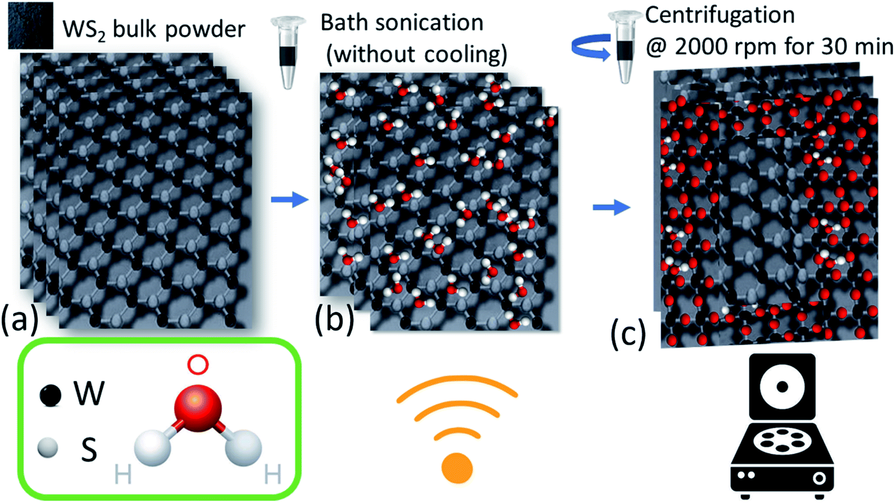 | ||
| Fig. 4 Schematic of (a) bulk WS2 powder existing in the form of layers (b) bath sonication in EtOH (only water molecules shown) without any additional effort to cool down the chamber and (c) sample centrifuged at 2000 rpm for 30 minutes. | ||
3.2. Gas sensing results
We utilized this nanomaterial as a sensing film in an IDE based chemiresistive device by simply dropcasting certain amount of the nanomaterial on IDE fingers. The device at a biasing voltage of 1 V shows stable baseline current in the range of few micro-ampere (μA). Then the device was subjected to several oxidizing and reducing gases and the ‘specificity (S)’ of the device was compared as per the histogram in Fig. 5(a). It should be noted here that the specificity (Si) of a chemiresistive device is the measure of how selectively a sensor can identify a particular analyte ‘i’ among a set of ‘n’ gases. Mathematically, it can be calculated as per eqn (2), where, Ii is the current in presence of analyte ‘i’ and Ia is the baseline current and numerical value of Si (0 ≤ Si ≤ 1) varies between zero to one (for 1 ≤ j ≤ n).24
 | (1) |
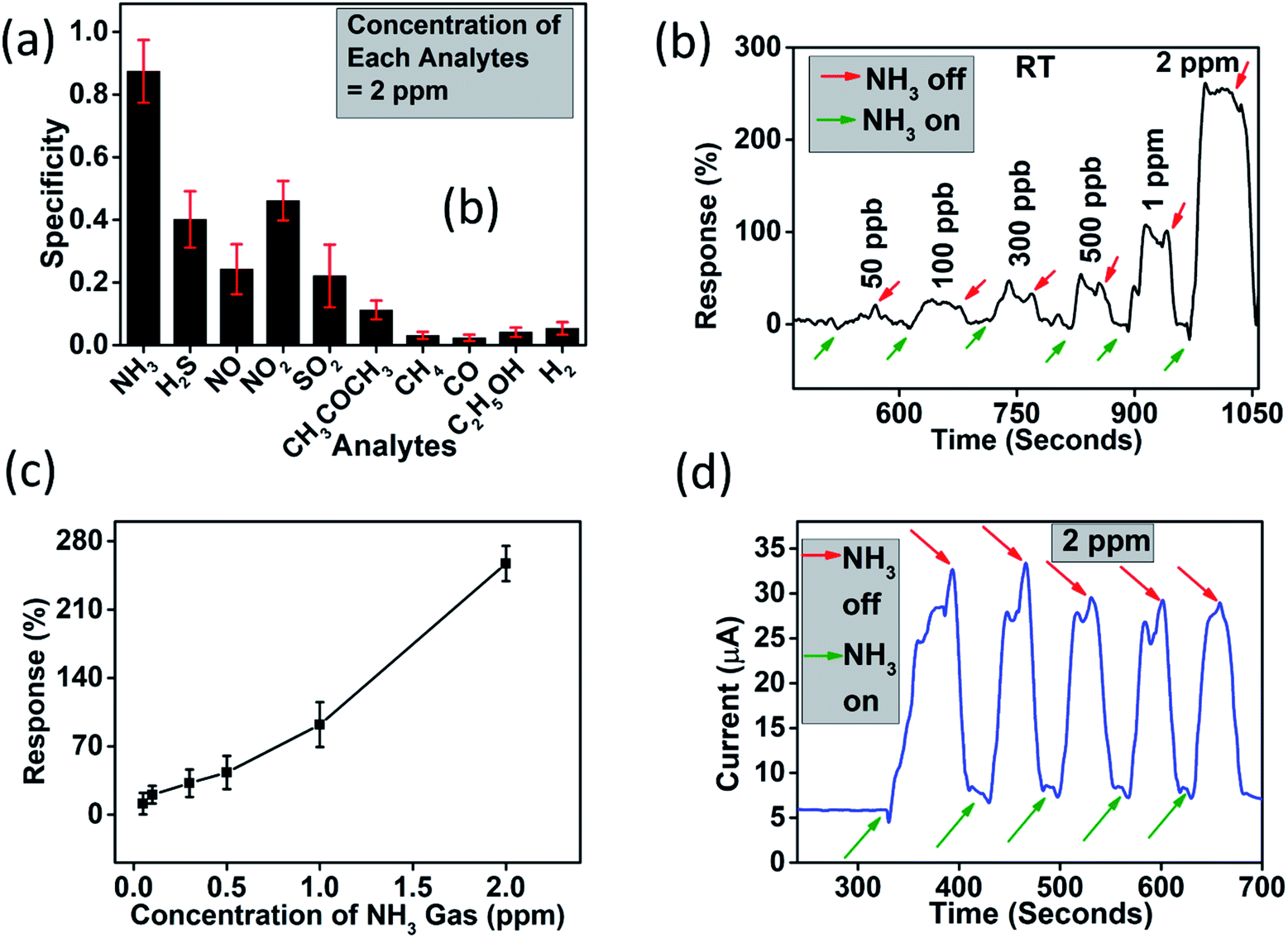 | ||
| Fig. 5 (a) Specificity of the device for six different analytes for 1 ppm concentration (b) response (%) for ammonia concentration 50 ppb to 2 ppm at room temperature (c) response vs. concentration (ppm) plot with an exponential fit with equation y = a/(1 + e − k*(x − xc)) (d) repeatability of 2 ppm ammonia concentration for five consecutive on–off cycles. | ||
It is clearly evident from Fig. 6(a) that among ten (n = 10) different analyte (NH3, H2S, NO, NO2, SO2, CH3COCH3 (acetone), CH4 (methane), CO, C2H5OH (ethyl alcohol), and H2), the device has highest specificity towards ammonia gas. Therefore, the device was subjected to different concentration of this analyte. Fig. 5(b) shows a dynamic response curve for when the device was subjected to ammonia concentration in the range 50 ppb to 2 ppm. The response (%) of the device was found to be 11.36–254.66% in this concentration range. It should be noted here that the response percentage of the sensor is calculated as
 | (2) |
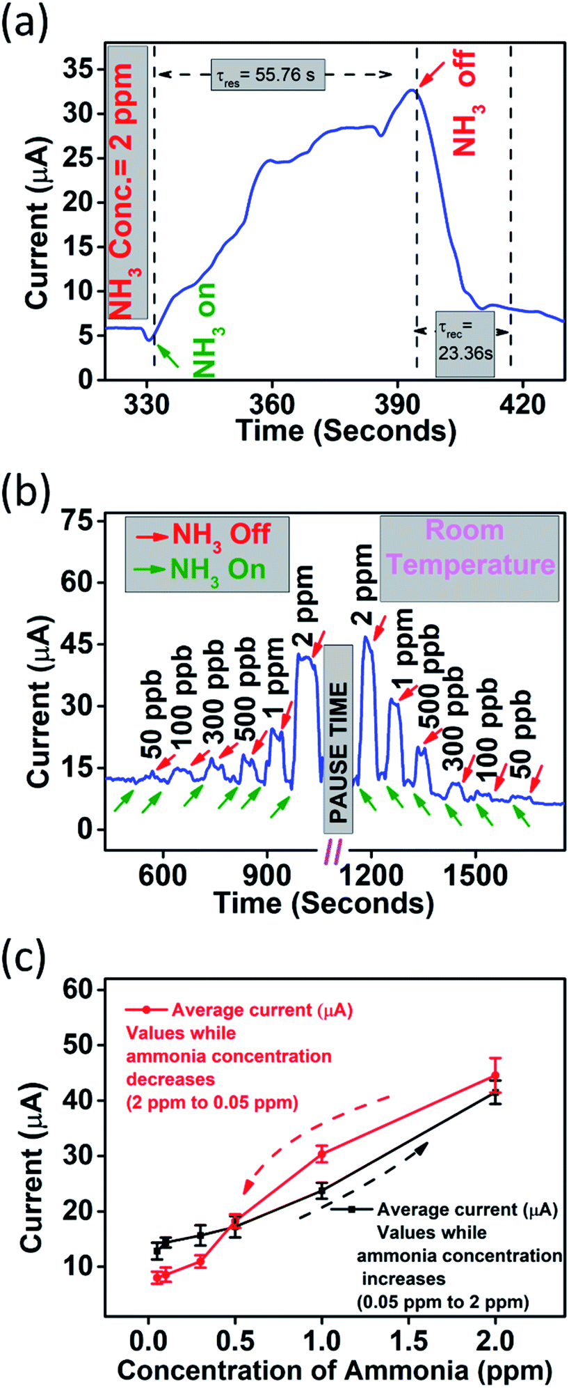 | ||
| Fig. 6 (a) Extraction of response time (τres) and recovery time (τrec) for 2 ppm ammonia concentration (b) variation in current over time when exposed to ammonia gas from 50 ppb to 2 ppm and back to 50 ppb in synthetic air and (c) corresponding hysteresis. | ||
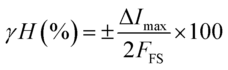
Hysteresis is an important issue in chemiresistive gas sensing method. We investigated hysteresis error associated with the device. Hysteresis error (%) is calculated as
 | (3) |
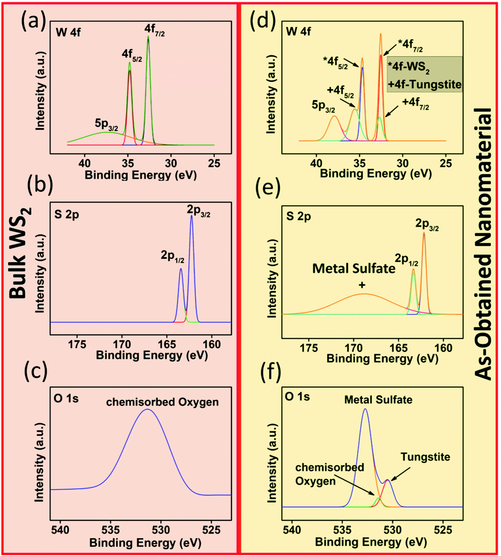 | ||
| Fig. 7 (a) Tungsten (W 4f), (b) sulfur (S 2p), (c) oxygen (O 1s) XPS spectra of bulk WS2 and (d) tungsten (W 4f), (e) sulfur (S 2p), (f) oxygen (O 1s) XPS spectra of as-obtained nanomaterial. | ||
We compared our result to some of the recent reported WS2 based ammonia gas sensors as shown in Table 1. Although, most of the reported WS2 and its hybrids/nanocomposites could detect ammonia at room temperature, but detecting below 1 ppm remains a challenge for them. WS2/WO3·H2O based device could detect much lower than this threshold at the same temperature. Also, the response and recovery time of our device is comparable to the reported results.
| Material | Measured ammonia range (in ppm) | Response (%) | Response time/recovery time (seconds) | Synthesis technique | Operating temp. | Ref. |
|---|---|---|---|---|---|---|
| WS2 | 1–10 | ∼225 @ 1 ppm | 120/150 @ 5 ppm | Ball milling of bulk WS2 | RT | 25 |
| WS2 | 1–5 | ∼0.22 @ 5 ppm | ∼300/600 @ 5 ppm | Plasma assisted synthesis at 500 °C | RT | 26 |
| WS2 | 0.05–3 | 4.3% @ 0.05 ppm | 147/14 @ 3 ppm | Liquid exfoliation | 250 °C | 27 |
| WS2/TiO2 | 20–500 | 43.72 @ 250 ppm | −/174.43 @ 30 ppm | Chemical synthesis | RT | 28 |
| WS2/RGO | 10–50 | 121 @ 10 ppm | 60/300 @ 30 ppm | Hydrothermal synthesis | RT | 29 |
| WS2/Pt | 50–750 | 3 @ 50 ppm | −/− | Hydrothermal synthesis | RT | 30 |
| WS2/WO3 | 250–2000 | 150 @ 200 ppm | 160/310 @ 1000 ppm | Liquid processing method | 250 °C | 31 |
| WS2/WO3·H2O | 0.05–2 | 11.36 @50 ppb | 55.76/23.36 @ 2 ppm | Liquid exfoliation method | This work |
We also compared WS2/WO3·H2O based ammonia sensor with other nanomaterials-based room temperature chemiresistive NH3 detectors (Table S1, (ESI)†) and found that our result is comparable to those.
3.3. Plausible mechanism
As it is predicted in the Fig. 4 as well as from experimental and theoretical predictions in earlier reports, the oxidation of the sheets happens from the edges, and hence, the edges of the nanosheets are considered to be tungstite for simplicity.32 Therefore, ideally there are three obvious sites where, the NH3 molecules could interact with the receptor film, they are: (i) at the tungsten sulfide surface (ii) at tungstite surface and (iii) at their interface.At the first interaction site, where NH3 molecule interact with WS2 surface, it is based on simple charge transfer mechanism as evident from the theoretical and experimental reports in literature.33 NH3 being a reducing gas, when it interacts with intrinsically n-type WS2 nano-surface, it donates electron to it. These electrons populate the majority carrier in WS2 which ultimately results in enhancement of current in presence of NH3 molecule as evident from the gas sensing results (as shown in Fig. 6(b)).
Another active site is the WO3·H2O nano-surface, which interacts with any analyte at its surface through ionized oxygen (present due to adsorption from the ambient).34 According to Wolkentein's model, the electron from the conduction band of WO3·H2O (which is a n-type semiconductor) is trapped by adsorbed surface O2 molecules and form a metastable oxygen ion (O2−(ads)) as per eqn (4) and (5).
| O2(gas) → O2(ads) | (4) |
| O2(ads) + e− → O2−(ads) [at room temperature] | (5) |
When NH3 molecule interacts with these oxygen ions the following series of reactions occur as
| NH3(gas) → NH3(ads) | (6) |
| 4NH3(ads) + 5O2−(ads) → 4NO + 6H2O + 5e− | (7) |
The electrons released in eqn (7) are released back to the conduction band of tungstite which leads to the increase in the density of electrons which results in increase in current in the sensor film.
The third possible active site is the interface of tungsten sulfide/tungstite. Due to the formation of depletion region at the n–n lateral heterojunction of the nanomaterial, the overall resistance of the material goes high. However, when the material is exposed to reducing gas like NH3, it transfers electron to the interface resulting in lowering the barrier potential and hence overall resistance.
Thus, interaction of NH3 molecule at all available active sites in the receptor film results in increase in current which is reflected in the sensing data. To understand the selectivity of WS2/WO3·H2O towards ammonia gas, we did chemical analysis of the sample using XPS as shown in Fig. 7. The tungsten (W 4f) XPS spectrum of exfoliated WS2 shows additional peaks corresponding to tungstite while the sulfur (S 2p) spectrum shows additional peaks at higher binding energy corresponding to surface sulfate (SO42−) which could form in the process of oxidation. The oxygen (O 1s) spectrum of the bulk WS2 shows a single peak corresponding to chemisorbed oxygen while the exfoliated sample has additional peaks due to presence of sulfate as well as tungstite. The presence of SO42− at the surface of nanomaterial, make it enriched in Lewis acid.28 These Lewis acid centers make it specific to the Lewis base gases like ammonia.35
4. Conclusions
To conclude, we have prepared WS2/WO3·H2O lateral heterostructure nanomaterial by ultrasonication, by simply altering the sonication condition and subsequent centrifugation. This nanomaterial was used as a receptor film to detect NH3 gas with high selectivity, in the concentration range of 50 ppb to 2 ppm. The response time and recovery time of the device was found to be of the order of tens of seconds. The repeatability, stability, and reproducibility of the device was found to be very good and comparable to the latest reports. We also proposed a sensing mechanism based on interaction of gas molecules at three different sites namely, the tungsten sulfide surface, tungstite surface and their interface. The proposed model is capable of explaining the sensing data, in the backdrop of material characterization results. This work will open a new possibility towards the fabrication of new heterostructure material based on metal sulfide/metal oxide for functional applications such as gas sensors.Conflicts of interest
There are no conflicts to declare.Acknowledgements
The authors acknowledge funding support from Ministry of Human Resource Development (MHRD) India, Ministry of Electronics and Information Technology (MeitY) India, Department of Science and Technology (DST) Nanomission, through Nanoelectronics Network for Research and Application (NNetRA). We also acknowledge the technical support provided by staff at National Nano Fabrication Facility (NNFC), and Micro and Nano Characterization Facility (MNCF) at Centre for Nano Science and Engineering (CeNSE), Indian Institute of Science (IISc) Bangalore, India. NB would also like to thank Indian National Academy of Engineering (INAE) and Science and Engineering Research Board (SERB) of DST for Abdul Kalam Technology Innovation National Fellowship. RJ acknowledge SERB for NPDF. We also thank Gayathry Thampi from Indian Institute of Science, Education, and Research (IISER), Berhampur, Odisha, India for her support in material preparation.Notes and references
- X. Xiao, X.-F. Cheng, X. Hou, J.-H. He, Q.-F. Xu, H. Li, N.-J. Li, D.-Y. Chen and J.-M. Lu, Small, 2017, 13, 1602190 CrossRef PubMed.
- B. R. Varju, S. A. Wollschlaeger and D. B. Leznoff, Chem.–Eur. J., 2019, 25, 9017–9025 CrossRef CAS PubMed.
- E. Rafatmah and B. Hemmateenejad, Electroanalysis, 2019, 31, 632–638 CrossRef CAS.
- K. S. Novoselov, A. Mishchenko, A. Carvalho and A. H. Castro Neto, Science, 2016, 353, aac9439 CrossRef CAS PubMed.
- D. Deng, K. S. Novoselov, Q. Fu, N. Zheng, Z. Tian and X. Bao, Nat. Nanotechnol., 2016, 11, 218–230 CrossRef CAS PubMed.
- X. Ling, Y. Lin, Q. Ma, Z. Wang, Y. Song, L. Yu, S. Huang, W. Fang, X. Zhang, A. L. Hsu, Y. Bie, Y.-H. Lee, Y. Zhu, L. Wu, J. Li, P. Jarillo-Herrero, M. Dresselhaus, T. Palacios and J. Kong, Adv. Mater., 2016, 28, 2322–2329 CrossRef CAS PubMed.
- X. Q. Zhang, C. H. Lin, Y. W. Tseng, K. H. Huang and Y. H. Lee, Nano Lett., 2015, 15, 410–415 CrossRef CAS PubMed.
- N. Sakhuja, R. Jha and N. Bhat, in Proceedings of IEEE Sensors, Institute of Electrical and Electronics Engineers Inc., 2018 October, vol. 2018 Search PubMed.
- R. K. Jha, J. V. D'Costa, N. Sakhuja and N. Bhat, Sens. Actuators, B, 2019, 297, 126687 CrossRef CAS.
- R. K. Jha, V. Singh, J. Sinha, S. Avasthi and N. Bhat, IEEE Sens. J., 2019, 19, 11759–11766 Search PubMed.
- K.-G. Zhou, N.-N. Mao, H.-X. Wang, Y. Peng and H.-L. Zhang, Angew. Chem., 2011, 123, 11031–11034 CrossRef.
- Y. Lin, B. Adilbekova, Y. Firdaus, E. Yengel, H. Faber, M. Sajjad, X. Zheng, E. Yarali, A. Seitkhan, O. M. Bakr, A. El-Labban, U. Schwingenschlögl, V. Tung, I. McCulloch, F. Laquai and T. D. Anthopoulos, Adv. Mater., 2019, 31, 1902965 CrossRef CAS PubMed.
- V. Nicolosi, M. Chhowalla, M. G. Kanatzidis, M. S. Strano and J. N. Coleman, Science, 2013, 340(6139), 1226419 CrossRef.
- J. N. Coleman, M. Lotya, A. O'Neill, S. D. Bergin, P. J. King, U. Khan, K. Young, A. Gaucher, S. De, R. J. Smith, I. V. Shvets, S. K. Arora, G. Stanton, H. Y. Kim, K. Lee, G. T. Kim, G. S. Duesberg, T. Hallam, J. J. Boland, J. J. Wang, J. F. Donegan, J. C. Grunlan, G. Moriarty, A. Shmeliov, R. J. Nicholls, J. M. Perkins, E. M. Grieveson, K. Theuwissen, D. W. McComb, P. D. Nellist and V. Nicolosi, Science, 2011, 331, 568–571 CrossRef CAS PubMed.
- C. Backes, B. M. Szydłowska, A. Harvey, S. Yuan, V. Vega-Mayoral, B. R. Davies, P. L. Zhao, D. Hanlon, E. J. G. Santos, M. I. Katsnelson, W. J. Blau, C. Gadermaier and J. N. Coleman, ACS Nano, 2016, 10, 1589–1601 CrossRef CAS PubMed.
- G. Q. Han, Y. R. Liu, W. H. Hu, B. Dong, X. Li, Y. M. Chai, Y. Q. Liu and C. G. Liu, Mater. Chem. Phys., 2015, 167, 271–277 CrossRef CAS.
- R. K. Jha, D. Burman, S. Santra and P. K. Guha, IEEE Sens. J., 2017, 17, 7340–7347 CAS.
- R. K. Jha and P. K. Guha, Nanotechnology, 2016, 27, 475503 CrossRef PubMed.
- B. D. Culity and S. R. Stock, Elements of X-ray diffraction, Edison-Wesley Publ. Co. Inc, USA, 2nd edn Search PubMed.
- L. Chen, T. Mashimo, H. Okudera, C. Iwamoto and E. Omurzak, RSC Adv., 2014, 4, 28673–28677 RSC.
- A. G. Kelly, V. Vega-Mayoral, J. B. Boland and J. N. Coleman, 2D Mater., 2019, 6, 45036 CrossRef CAS.
- M. Ahmadi and M. J. F. Guinel, Acta Mater., 2014, 69, 203–209 CrossRef CAS.
- G. Pagona, C. Bittencourt, R. Arenal and N. Tagmatarchis, Chem. Commun., 2015, 51, 12950–12953 RSC.
- R. K. Jha, N. Sakhuja, S. Jakhar and N. Bhat, IEEE Trans. Nanotechnol., 2019, 18, 932–939 CAS.
- X. Li, X. Li, Z. Li, J. Wang and J. Zhang, Sens. Actuators, B, 2017, 240, 273–277 CrossRef CAS.
- M. O'Brien, K. Lee, R. Morrish, N. C. Berner, N. McEvoy, C. A. Wolden and G. S. Duesberg, Chem. Phys. Lett., 2014, 615, 6–10 CrossRef.
- N. Sakhuja, R. K. Jha and N. Bhat, IEEE Sens. J., 2019, 19, 11767–11774 Search PubMed.
- Z. Qin, C. Ouyang, J. Zhang, L. Wan, S. Wang, C. Xie and D. Zeng, Sens. Actuators, B, 2017, 253, 1034–1042 CrossRef CAS.
- X. Wang, D. Gu, X. Li, S. Lin, S. Zhao, M. N. Rumyantseva and A. M. Gaskov, Sens. Actuators, B, 2019, 282, 290–299 CrossRef CAS.
- C. Ouyang, Y. Chen, Z. Qin, D. Zeng, J. Zhang, H. Wang and C. Xie, Appl. Surf. Sci., 2018, 455, 45–52 CrossRef CAS.
- R. K. Jha, M. Wan, C. Jacob and P. K. Guha, IEEE Sens. J., 2018, 18, 3494–3501 CAS.
- P. Zhou, Q. Xu, H. Li, Y. Wang, B. Yan, Y. Zhou, J. Chen, J. Zhang and K. Wang, Angew. Chem., Int. Ed., 2015, 54, 15226–15230 CrossRef CAS PubMed.
- C. Zhou, W. Yang and H. Zhu, J. Chem. Phys., 2015, 142, 214704 CrossRef PubMed.
- F. Li, S. Guo, J. Shen, L. Shen, D. Sun, B. Wang, Y. Chen and S. Ruan, Sens. Actuators, B, 2017, 238, 364–373 CrossRef CAS.
- S. Kabcum, N. Kotchasak, D. Channei, A. Tuantranont, A. Wisitsoraat, S. Phanichphant and C. Liewhiran, Sens. Actuators, B, 2017, 252, 523–536 CrossRef CAS.
Footnote |
| † Electronic supplementary information (ESI) available. See DOI: 10.1039/d0ra02553d |
| This journal is © The Royal Society of Chemistry 2020 |