
 Open Access Article
 This Open Access Article is licensed under a Creative Commons Attribution-Non Commercial 3.0 Unported Licence
Stability studies of ZnO and AlN thin film acoustic wave devices in acid and alkali harsh environments
Shuo Xionga,
Xudong Liua,
Jian Zhou *a,
Yi Liub,
Yiping Shenb,
Xiaobo Yina,
Jianhui Wua,
Ran Taoc,
Yongqing Fuc and
Huigao Duana
*a,
Yi Liub,
Yiping Shenb,
Xiaobo Yina,
Jianhui Wua,
Ran Taoc,
Yongqing Fuc and
Huigao Duana
aState Key Laboratory of Advanced Design and Manufacturing for Vehicle Body, College of Mechanical and Vehicle Engineering, Hunan University, Changsha 410082, China. E-mail: jianzhou@hnu.edu.cn
bHunan Provincial Key Laboratory of Health Maintenance for Mechanical Equipment, Hunan University of Science and Technology, Xiangtan 411201, China
cFaculty of Engineering and Environment, Northumbria University, Newcastle upon Tyne, NE1 8ST, UK
First published on 20th May 2020
Abstract
Surface acoustic wave (SAW) devices based on piezoelectric thin-films such as ZnO and AlN are widely used in sensing, microfluidics and lab-on-a-chip applications. However, for many of these applications, the SAW devices will inevitably be used in acid or alkali harsh environments, which may cause their early failures. In this work, we investigated the behavior and degradation mechanisms of thin film based SAW devices in acid and alkali harsh environments. Results show that under the acid and alkali attacks, chemical reaction and corrosion of ZnO devices are very fast (usually within 45 s). During the corrosion, the crystalline orientation of the ZnO film is not changed, but its grain defects are significantly increased and the grain sizes are decreased. The velocity of ZnO-based SAW devices is decreased due to the formation of porous structures induced by the chemical reactions. Whereas an AlN thin-film based SAW device does not perform well in acid–alkali conditions, it might be able to maintain a normal performance without obvious degradation for more than ten hours in acid or alkali solutions. This work could provide guidance for the applications of both ZnO or AlN-based SAW devices in acid/alkali harsh environments.
1 Introduction
Piezoelectric thin-film acoustic wave technology, based on materials such as ZnO or AlN, is attractive for acoustic wave based sensing, microfluidics and lab-on-a-chip devices.1–4 With thin-films deposited onto various substrates including silicon, glass, metal plates/foils and polymer/plastics, flexibility in designs and wide range applications become achievable. Film based surface acoustic wave (SAW) sensors (such as temperature, humidity, UV, and gas), and microfluidic applications (streaming, pumping, jetting and nebulization) have been widely reported.5–8In some of these applications, the film surface of the SAW devices needs to be in direct contact with the targeted objects during either sensing or microfluidic processes. For example, when the SAW device is used to detect hydrogen fluoride, hydrochloric acid, uric acid detection and pH value9–11 or is used as an actuator for a lab-on-chip in a biochemical environment, the SAW device will be exposed to an acid/alkali harsh environment. Therefore, the quick failure of film based acoustic wave devices caused by chemical reactions often becomes a critical issue.
It is well known that ZnO film based SAW devices do not show good tolerance with acid and alkali, but AlN film based SAW devices have excellent chemical stability.12 However, many questions are remained to be answered. For examples, are the AlN based SAW devices able to used in both acid and alkali harsh environments? How long will these ZnO and AlN based SAW devices can functionize well in acid/alkali harsh environment? What are the corrosion mechanisms and reaction processes of ZnO and AlN based SAW devices in acid/alkali harsh environment? Or how does the SAW devices perform (e.g., changes of signal amplitude, frequency or acoustic wave velocity) during the reaction process? Most of these issues have not been reported in literature.
In this work, for the first time, we present a systematic and extensive investigation to explore the performance of ZnO and AlN based SAW devices in both acid and alkali harsh environments. Results show that under the acid and alkali attacks, chemical reactions and corrosion of ZnO SAW devices are very fast (usually within 45 s). During the corrosion process, the velocity of ZnO-based SAW devices is decreased significantly due to the generation of porous film structures. AlN thin-film based SAW device is also not well performed in acid–alkali conditions, although they might be able to maintain normal performance without obvious degradation for more ten hours in acid or alkali solutions.
2 Experimental
ZnO films with a thickness of ∼3 μm were deposited onto 4 inch glass substrates (Corning glass), using a DC reactive magnetron sputtering process in an ultra-high vacuum system. The base pressure of the chamber was 1 × 10⁻⁴ Pa before deposition. A zinc target with a purity of 99.99% was used during deposition. The surface of the substrate was pre-cleaned by means of a short bombardment (10 min) with Ar+ ions using a DC power of 300 W. The deposition conditions were as follows: DC sputtering power of 250 W, O2/Ar mixing flow ratio of 50/50 sccm, deposition rate of ∼500 nm per hour with a deposition pressure of 2 Pa, substrate temperature of 100 °C.AlN films with a thick of ∼2 μm were deposited onto (0001) sapphire substrates using an RF magnetron sputter. Prior to the deposition, the sapphire substrate was cleaned in an ultrasonic bath with acetone, absolute ethyl alcohol and deionized water in a sequence. The base vacuum of the sputter chamber was ∼1 × 10⁻⁴ Pa. The deposition conditions were as follows: RF sputtering power of 350 W, N2/Ar mixing flow ratio of 12/24 sccm; deposition rate of ∼500 nm per hour with a deposition pressure of 0.5 Pa, substrate temperature of 300 °C.
Crystal orientation of the films and those films after exposed to different acid and alkali solutions were analyzed using X-ray diffraction (XRD, D5000, Siemens) with Cu-Kα radiation (λ = 1.5406 Å). The diffraction patterns were obtained in the 2θ model with scanned angle range of 2θ = 20°–70° and a step of 0.02°. Crystal sizes of the films were estimated using the Debye–Scherrer formula:13,14
D = Kλ/(β![[thin space (1/6-em)]](https://www.rsc.org/images/entities/char_2009.gif) cosθ) cosθ)
| (1) |
Two-port SAW resonators (as shown in Fig. 1) were designed and fabricated using laser direct writing photolithography and lift-off processes. Compared with the conventional ultraviolet (UV) lithography, the laser direct writing photolithography doses not need a mask and can be used in real-time, thus the patterns with random shapes can be directly generated. The wavelength of laser direct writing photolithography was 405 nm, with a writing speed of 15 mm2 min−1 and a structure resolution of 1 μm. For the SAW devices, Cr/Au was used as the electrodes (with a thickness of 1 nm/30 nm) and each SAW transducer was consisted of 80 pairs of IDT (Interdigital Transducers) fingers, with wavelengths λ of 12 and 20 μm. The distance between the two IDT transducers was 2.75 λ. The aperture was 20 λ and the distance between the IDTs and the adjacent shorted reflecting gratings was designed to be 1/4 λ to ensure the formation of a standing wave at the resonant frequency. The transmission characteristics were measured using an Agilent Technologies E5061B network analyzer.
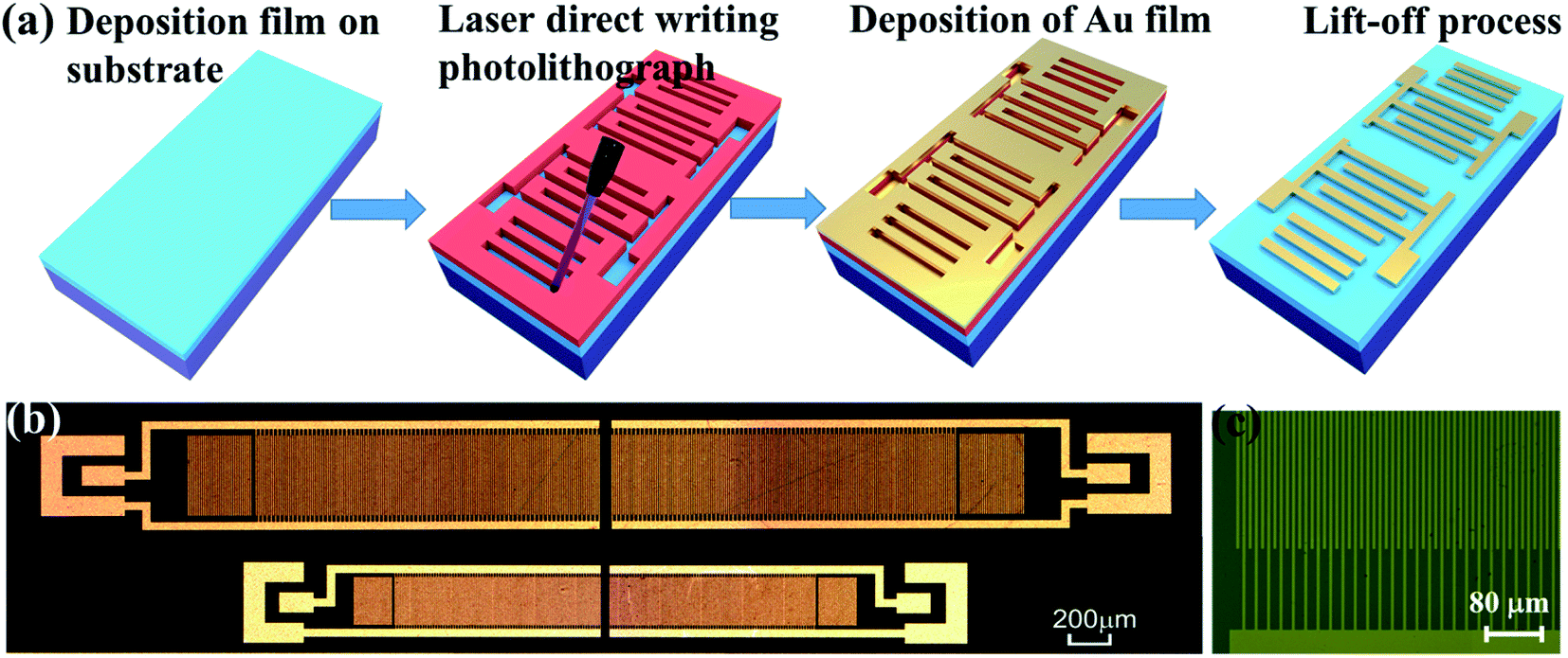 | ||
| Fig. 1 (a) Schematic illustration of device fabrication processes based on laser direct writing photolithography; (b) optical images of fabricated ZnO SAW devices with wavelength of 12 μm and 20 μm using laser direct writing photolithography, showing the whole device structure; (c) optical images of fabricated IDTs of ZnO SAW devices with wavelength of 20 μm. | ||
For the acid/alkaline tests, the ZnO SAW device was placed into 1% HCl solution and 20% NaOH solution, respectively, with the controlled exposure time. Then the devices were quickly cleaned with the deionized water to stop the reaction and dried using nitrogen gas. Different characterizations (including SEM, XRD, Raman diffraction, and network analyzer) were performed after each chemical treatment.
3 Results and discussion
Fig. 2(a) and (b) show optical images of ZnO based SAW devices at various durations in HCl and NaOH solutions. Results show that the ZnO thin film reacts rapidly in the HCl solution as shown in Fig. 2(a). As the reaction progresses, ZnO film was gradually dissolved and at the time of ∼15 s, the IDT structure began to disappear from the substrate due to the dissolution of ZnO film. Fig. 2(b) shows the ZnO SAW device surface when exposed to alkali environments (NaOH solution), and clearly the film cannot endure the alkali environment up to 45 s. However, unlike those behavior in the acid environment which is a continuous chemical reaction process, for the ZnO films in the alkali environment, at the beginning of the reaction (from 0 s to 40 s), the film did not change significantly. However, after 40 s, the film was quickly etched, and then peeled off from the substrate within 45 s.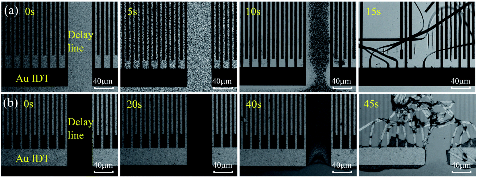 | ||
| Fig. 2 (a) Optical images of different reaction time of ZnO device in HCl solution. (b) Optical photos of different reaction time of ZnO device in NaOH solution. | ||
ZnO is an amphoteric oxide, and can easily react with strong acid/alkali solutions. The relevant reaction reactions are listed as follows:15
| ZnO + 2H+ → Zn2+ + H2O | (2) |
| ZnO + 2OH− → ZnO22− + H2O | (3) |
These cause the ZnO film to be dissolved into the acid/alkali solutions rapidly. However, in the alkali solution, the ZnO film will form ZnO22− ions and will be further hydrolyzed to form a precipitate of Zn(OH)2.16 This may protect the ZnO structure to a certain extent at the early corrosion stage.
To further investigate the detailed reaction processes, XRD analysis of the ZnO films after left in the HCl and NaOH solutions at different durations were performed and the results are shown in Fig. 3(a) and (b). The deposited ZnO thin film has a peak at 2θ values of 34.05° on the XRD pattern, corresponding to the peak of ZnO (0002) orientation. As the reaction proceeds, the peak positions of all the films do not show apparent changes, demonstrating that acidic and alkali attacks will not change the film orientation. However, with the corrosion time increases, the intensities of (0002) orientation peaks of the ZnO films are gradually decreased, showing that the film are gradually etched and more defects are generated with the acidic and alkali corrosion. We also calculated crystalline sizes of ZnO films after the reaction using MDI Jade 6 software. Fig. 3(c) and (d) show that the crystal sizes of the ZnO thin film seem to be reduced after the reactions with the acid/alkali solutions.
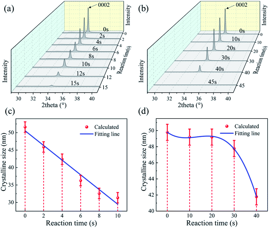 | ||
| Fig. 3 XRD patterns of ZnO film in (a) HCl solution and (b) NaOH solution with the time; crystalline size of ZnO film in (c) HCl solution and (d) NaOH solution with the time. | ||
Fig. 4 shows the crystal quality of the ZnO films analyzed using the Raman spectroscopy. The peaks of 434 and 576 cm−1 in the Raman spectra are observed, corresponding to the acoustic overtones of E2H and ELO1 for ZnO, respectively. The Raman peak around 1150 cm−1 is also observed, which is corresponding to the optical overtone of the ZnO.17 There is a slight decrease for Raman peaks during the corrosion, due to the deteriorated ZnO crystal quality in the acid/alkali harsh environments, although the changes are not so significant. The reason may be attributed to that the intensity of Raman peaks reflects the nature of crystal bonding quality, which does not change significantly during the corrosion of ZnO films.
 | ||
| Fig. 4 Raman spectra of ZnO film in (a) HCl solution and (b) NaOH solution. | ||
Fig. 5 show SEM images of surface morphology evolutions of ZnO thin film in the HCl and NaOH solutions at different corrosion durations. Without any corrosion of acid and alkali environment, the ZnO thin film shows dense crystal grains and a large crystalline size. With the corrosions in HCl and NaOH solutions, the surface morphology of the film exhibits significant defects, and the films become porous. The surface feature sizes become smaller, which is consistent with the XRD results of film as shown in Fig. 3(c) and (d).
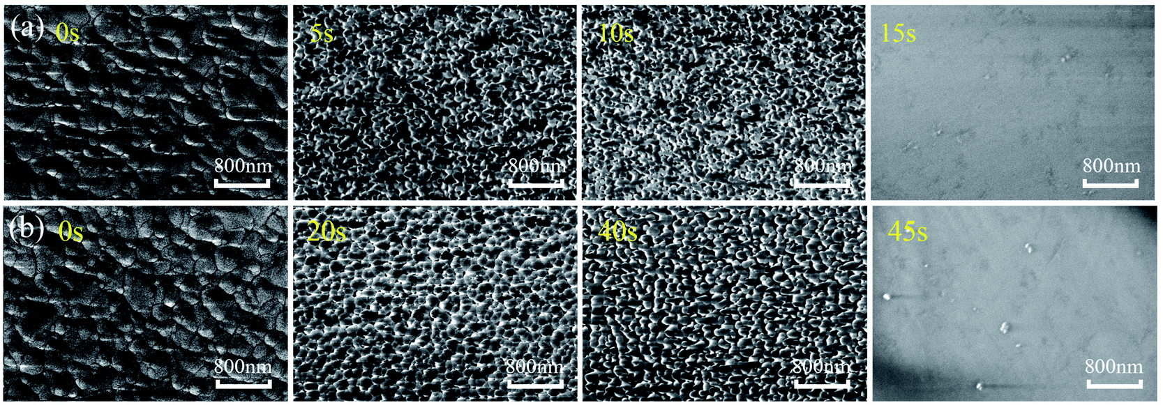 | ||
| Fig. 5 SEM images of ZnO film in (a) HCl solution and (b) NaOH solution at different time. | ||
Fig. 6 shows the transmission (S21) and reflection (S11) spectra of the ZnO/glass based SAW devices with the wavelengths of 12 and 20 μm after the acid reaction. It is clear that, without any reaction (time of 0 s), the SAW devices present two modes (e.g., the Mode 0-Rayleigh and Mode 1-Sezawa) for the devices with wavelengths of 12 and 20 μm. The corresponding resonant frequencies, f0 and f1 are 213.84, 425.93 MHz and 133.95, 265.25 MHz, respectively.
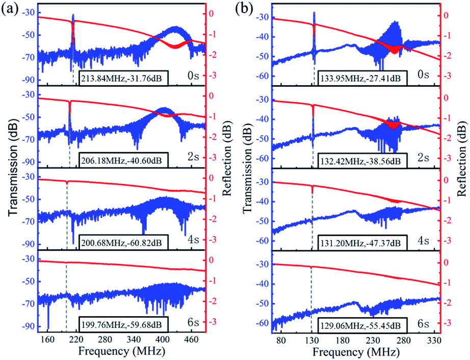 | ||
| Fig. 6 Frequency response of ZnO based SAW devices in HCl solution with wavelength of (a) 12 μm and (b) 20 μm. | ||
As the ZnO film reacts with the HCl solution, both signal amplitudes of two modes are decreased rapidly whereas the values of insertion loss are increased for both the devices with wavelengths of 12 and 20 μm. This indicates that the ZnO based SAW device is particularly sensitive to corrosion in the HCl solution. The acid solution will affect the quality of ZnO film thus finally deteriorate the device performance.
The phase velocities (vp) of ZnO SAW devices can be calculated using the formula, vp = λf, where λ is the wavelength and f is resonance frequency. The velocities of Rayleigh wave and Sezawa modes were calculated to be 2566.1 m s−1 and 5111.2 m s−1 for λ of 12 μm and to be 2679 m s−1 and 5305 m s−1 for λ of 20 μm, respectively. The Rayleigh phase velocity of the pure ZnO is ∼2500 m s−1,18 whereas that for the Rayleigh wave in glass is 3200 m s−1,19 which is larger than that of ZnO film. When the wavelength is decreased, more energy is confined within the ZnO film, thus resulting in a lower velocity of wave propagation, and leading to a lower velocity of the layered structure. This is consistent with the observation from other layered structure SAW devices.20
As in the case of ZnO film in the HCl solution, the signal amplitude and insertion loss of SAW devices are also deteriorated in the NaOH solution as shown in Fig. 7. An interesting phenomenon is that with the progression of corrosion in the NaOH solution, the resonant frequencies are gradually decreased for two devices with wavelengths of 12 μm and 20 μm. We have also characterized the films in the HCl solutions, the results show the same trends, which clearly indicates that after the devices are etched inside the acid and alkali environments the resonant frequency was decreased. As the phase velocity of the ZnO is smaller than that of glass substrate, therefore when the acid and alkali solutions corrode the ZnO film, more energy is confined in the glass which has a higher velocity. This should lead to a larger velocity of the layered structure and a positive frequency shift. However, the experimental results show an opposite shift in frequency.
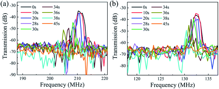 | ||
| Fig. 7 Response frequency of ZnO devices in NaOH solution with the wavelength of (a) 12 μm and (b) 20 μm. | ||
The frequency shifts of SAW sensor is mainly dependent on the following three factors: mass load, elastic changes in elasticity and acousto-electric interaction.21,22 The equation representing the contributions of these three factors is:
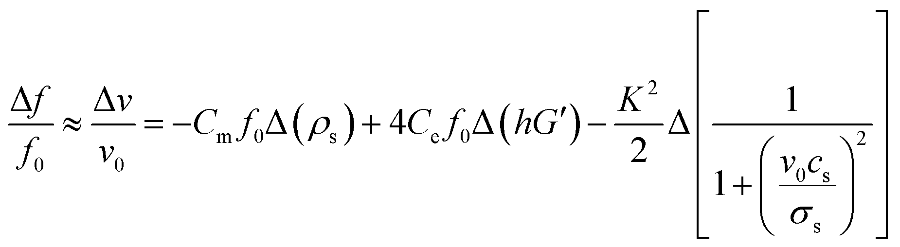 | (4) |
In this study, ions and reaction products adsorbed by the film are dissolved in the solution without accumulation on the surface of the film, so the contribution of the acoustic electric effect to the frequency shift can be ignored. Moreover, film thinning should result in a positive frequency shift. The main cause of the frequency shift in this case might be from the elastic change of the film. Fig. 5 shows that with the process of acid and alkali corrosion, the film becomes porous, and the grain size and density of film are decreased. These will result in the reduction of film shear modulus, softening of film and thus reduction of the sound velocity. Therefore the item of Δ(hG′) in eqn (4) becomes smaller, which results in a negative shift in frequency.
In order to verify this, we have performed simulations of SAW using the finite element analysis (FEA) with the commercial COMSOL 5.4 software in a two-dimensional (2D) piezo plane strain mode. The simulation method and parameters can be referred to our previous work.12 Fig. 8(a) shows the simulation results of surface displacements and frequency response of ZnO based SAW devices with a wavelength of 12 μm. It is clear that the simulated results are compatible with the experimental ones. With the thickness of ZnO film deceased from 3 μm to 2 μm, the frequency becomes larger (Fig. 8(b)). This shows that with the corrosion of ZnO film, film thinning effect should result in a positive frequency shift, which in this study, we obtained the opposite effect experimentally. Therefore, the main cause for the decrease of frequency should be the formation of porous film and the elastic change of the film.
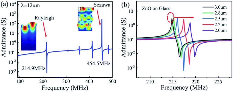 | ||
| Fig. 8 (a) Simulation results of frequency response and wave mode of ZnO based SAW device with the wavelength of 12 μm using COMSOL Multiphysics; (b) the Simulation results of resonance frequency shifts of ZnO based SAW device with the ZnO thickness from 2 μm to 3 μm. | ||
We have also fabricated the AlN film based SAW devices and studied their performance in both acid and alkali environments. Fig. 9(a) and (b) show optical images of AlN based SAW device at various durations in HCl and NaOH solutions. Results show that the AlN thin film also reacts in the HCl solution as shown in Fig. 9(a). As the reaction progresses, IDT structure of AlN based SAW device shows obvious damage due to the dissolution of AlN film after 12 h. Fig. 9(b) shows the optical image of AlN film when exposed to the alkali environment (e.g., the NaOH solution). Results showed that AlN film cannot endure the alkali environment after 10 min. These results are very interesting, as it is normally regarded that the AlN film has excellent chemical stability and should withstand the corrosion for quite a long time. Although compared with those of ZnO ones, these AlN SAW devices can have good performance without obvious degradation for more ten hours in acid or alkali solution. One of the explanations could be that the deposited AlN film has a vertical columnar structures. Therefore, the corrosion easily occurred vertically along the columnar boundaries of the AlN films.
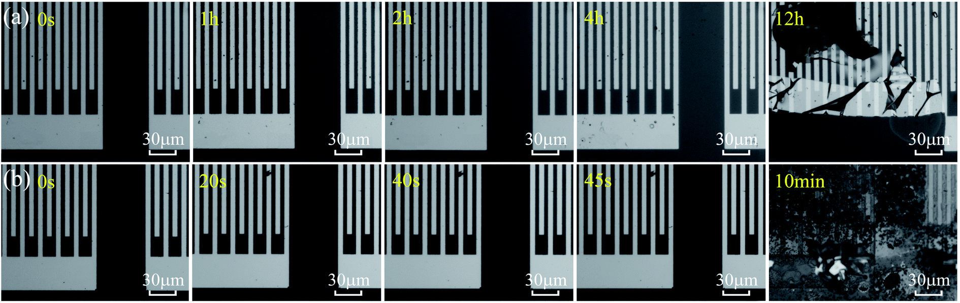 | ||
| Fig. 9 (a) Optical images of different reaction time of AlN device in HCl solution. (b) Optical photos of different reaction time of ZnO device in NaOH solution. | ||
Actually, AlN can react with acid and alkali solutions, and the reaction equations are listed as follows:23,24
| 2AlN + 8H+ → 2Al3+ + 2NH4+ | (5) |
| AlN + 3H2O → Al(OH)3↓ + NH3↑ | (6) |
| AlN + OH− + H2O → AlO2− + NH3↑ | (7) |
These reactions cause the AlN film to be dissolved into the acid/alkali solutions.
To further investigate the detailed reaction processes, XRD analysis of the AlN films after left in the HCl and NaOH solutions at different reaction durations were performed and the results are shown in Fig. 10(a) and (b). The deposited AlN thin film has a strong (0002) orientation. Similar to that of ZnO film, as the corrosion reaction proceeds, the intensities of (0002) peak of the AlN films are gradually decreased, showing that the film are gradually etched and more defects are generated with the time of acidic and alkali corrosion.
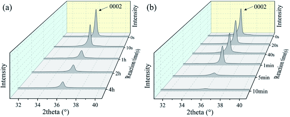 | ||
| Fig. 10 XRD patterns of AlN film in (a) HCl solution and (b) NaOH solution with the time. | ||
Fig. 11 shows the transmission (S21) and reflection (S11) spectra of the AlN/sapphire based SAW devices after the acid and alkali reactions. Compared with those of the ZnO films, the AlN SAW device has a much better performance in HCl solution, and there is no obvious deterioration in SAW signal and performance after 4 hours. However, the device has lost the SAW signals at 12 hours. On the other hand, in the NaOH solution, the tolerance characteristics of AlN device is relatively poorer, and the device has completely failed after 10 min. This clearly indicates that although the resistance of AlN film to extreme environment is much better than that of ZnO device, the AlN film based SAW device still face the problem of corrosion at the acid and alkali environments when they are used for sensing and biological lab on chip.
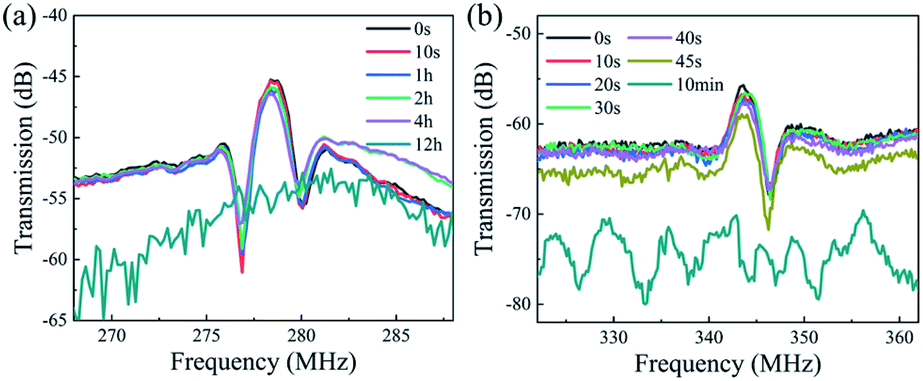 | ||
| Fig. 11 Frequency response of AlN devices in (a) HCl solution and (b) NaOH solution with the time. | ||
4 Conclusion
Surface acoustic wave (SAW) devices based on piezoelectric thin-films such as ZnO and AlN are widely used in sensing, microfluidics and lab-on-a-chip. However, for some sensing application such as pH sensing, or microfluidics and biological lab-on-chips, the SAW devices may inevitably encounter acid or alkali extreme environments, which may cause the failure of devices. This paper, for the first time, investigated the performance and mechanism of thin film based SAW devices in acid–alkali harsh environments.With the acid and alkali corrosion proceeds, chemical reaction of ZnO is very fast and it cannot endure more than 45 s. Film crystalline orientation was not changed, but the grain defects were increased and the grain size was decreased during the corrosion process. The acoustic velocity of piezoelectric film based SAW devices was also decreased due to the formation of porous structures of film, thus the film shear modulus becomes smaller and film becomes porous.
In addition, AlN thin-film based SAW device is also not well performed in acid–alkali conditions, although they might be able to maintain a good performance without obvious degradation for more ten hours in acid or alkali solution. This study could provide a guidance for the application of both ZnO or AlN-based SAW devices in the acid/alkali harsh environments.
Conflicts of interest
There are no conflicts to declare.Acknowledgements
This work was supported by the Key Research Project of Hunan Province (2019GK2111, 2018GK2044). The UK Engineering and Physical Sciences Research Council (EPSRC) grants EP/P018998/1, Newton Mobility Grant (IE161019) through Royal Society and the National Natural Science Foundation of China. The authors acknowledge Engineering Research Center of Automotive Electronics and Control Technology of Ministry of Education and National Engineering Research Centre for High Efficiency Grinding.References
- L. Rana, R. Gupta, M. Tomar and V. Gupta, Sens. Actuators, B, 2017, 252, 840–845 CrossRef CAS.
- A. J. Flewitt, J. K. Luo, Y. Q. Fu, L. Garcia-Gancedo, X. Y. Du, J. R. Lu, X. B. Zhao, E. Iborra, M. Ramos and W. I. Milne, J. Non-Newtonian Fluid Mech., 2015, 222, 209–216 CrossRef.
- G. Destgeer, A. Hashmi, J. Park, H. Ahmed, M. Afzal and H. J. Sung, RSC Adv., 2019, 9, 7916 RSC.
- F. M. Mwema, E. T. Akinlabi and O. P. Oladijo, Mater. Today: Proc., 2020 DOI:10.1016/j.matpr.2020.02.317.
- A. Ghosh, C. Zhang, S. Shi and H. Zhang, Sens. Actuators, B, 2019, 301, 126958 CrossRef CAS.
- X. Le, X. Wang, J. Pang, Y. Liu, B. Fang, Z. Xu, C. Gao, Y. Xu and J. Xie, Sens. Actuators, B, 2018, 255, 2454–2461 CrossRef CAS.
- J. Zhou, M. DeMiguel-Ramos, L. Garcia-Gancedo, E. Iborra, J. Olivares, H. Jin, J. K. Luo, A. S. Elhady, S. R. Dong, D. M. Wang and Y. Q. Fu, Sens. Actuators, B, 2014, 202, 984–992 CrossRef CAS.
- X. L. He, J. Zhou, W. B. Wang, W. P. Xuan, X. Yang, H. Jin and J. K. Luo, J. Micromech. Microeng., 2014, 24, 055014 CrossRef.
- L. Rana, R. Gupta, M. Tomar and V. Gupta, Sens. Actuators, B, 2018, 261, 169–177 CrossRef CAS.
- T. Wang, R. Green, R. Guldiken, S. Mohapatra and S. Mohapatra, Biosens. Bioelectron., 2019, 124–125, 244–252 CrossRef CAS PubMed.
- B. J. Meulendyk, Design, fabrication, and testing of saw resonators on quartz for the detection of hydrogen fluoride, The University of Maine, 2011 Search PubMed.
- J. Zhou, H. F. Pang, L. Garcia-Gancedo, E. Iborra, M. Clement, M. De Miguel-Ramos, H. Jin, J. K. Luo, S. Smith, S. R. Dong, D. M. Wang and Y. Q. Fu, Microfluid. Nanofluidics, 2015, 18, 537–548 CrossRef CAS.
- W. L. Dang, Y. Q. Fu, J. K. Luo, A. J. Flewitt and W. I. Milne, Superlattice. Microst., 2007, 42, 89–93 CrossRef CAS.
- G. K. Mani, M. Morohoshi, Y. Yasoda, S. Yokoyama, H. Kimura and K. Tsuchiya, ACS Appl. Mater. Interfaces, 2017, 9, 5193–5203 CrossRef CAS PubMed.
- J. Han, W. Qiu and W. Gao, J. Hazard. Mater., 2010, 178, 115–122 CrossRef CAS PubMed.
- R. A. McBride, J. M. Kelly and D. E. McCormack, J. Mater. Chem., 2003, 13, 1196–1201 RSC.
- Y. Liu, J. T. Luo, C. Zhao, J. Zhou, S. A. Hasan, Y. F. Li, M. Cooke, Q. Wu, W. P. Ng, J. F. Du, Q. Yu, Y. Liu and Y. Q. Fu, IEEE Trans. Electron Devices, 2016, 63, 4535–4541 CAS.
- P. Dutheil, J. C. Orlianges, A. Crunteanu, A. Catherinot and C. Champeaux, Phys. Status Solidi A, 2015, 212, 817–825 CrossRef CAS.
- J. Zhou, X. L. He, W. B. Wang, Q. Zhu, W. P. Xuan, H. Jin, S. R. Dong, D. M. Wang and J. K. Luo, IEEE Electron Device Lett., 2013, 34, 1319–1321 CAS.
- M. Kadota and C. Kondoh, IEEE Trans. Ultrason. Ferroelectrics Freq. Contr., 1997, 44, 658–665 Search PubMed.
- M. Li, H. Kan, S. Chen, X. Feng, H. Li, C. Li, C. Fu, A. Quan, H. Sun, J. Luo, X. Liu, W. Wang, H. Liu, Q. Wei and Y. Fu, Sens. Actuators, B, 2019, 287, 241–249 CrossRef CAS.
- J. D. Galipeau, R. S. Falconer, J. F. Vetelino, J. J. Caron, E. L. Wittman, M. G. Schweyer and J. C. Andle, Sens. Actuators, B, 1995, 24, 49–53 CrossRef CAS.
- Y. Zhang and J. G. P. Binner, Int. J. Inorg. Mater., 1999, 1, 219–227 CrossRef CAS.
- L. M. Svedberg, K. C. Arndt and M. J. Cima, J. Am. Ceram. Soc., 2000, 83, 41–46 CrossRef CAS.
| This journal is © The Royal Society of Chemistry 2020 |