
 Open Access Article
 This Open Access Article is licensed under a Creative Commons Attribution-Non Commercial 3.0 Unported Licence
Atomic and electronic structures of charge-doping VO2: first-principles calculations
Lanli Chen ab,
Yuanyuan Cuib,
Hongjie Luob and
Yanfeng Gao*bc
ab,
Yuanyuan Cuib,
Hongjie Luob and
Yanfeng Gao*bc
aSchool of Mathematics and Physics, Hubei Polytechnic University, Huangshi 435003, China
bSchool of Materials Science and Engineering, Shanghai University, Shanghai 200444, China. E-mail: yfgao@shu.edu.cn
cFaculty of Chemical Engineering, Huaiyin Institute of Technology, Jiangsu 223003, China
First published on 15th May 2020
Abstract
The atomic and electronic structures of charge-doping VO2 are investigated by using first-principles calculations. Hole doping is more conducive to stabilizing the structure of VO2 than electron doping. The controllable phase transition temperature is coupled with changes in atomic and electronic structures. With the increase in hole density, the V–V chains and twisting angle experience a dramatic change, and the band gap (0.69–0 eV) is rapidly reduced due to orbital switching between the dx2−y2 and dz2/dyz orbitals. However, as the electron density increases, the band gap (0.69–0.502 eV) narrows slightly, while the V–O bond lengths significantly increase. The current results provide up a variable way to tune the VO2 phase transition temperature through charge-doping.
1. Introduction
Vanadium dioxide (VO2) is an attractive thermochromic material due to its reversible metal–insulator transition (MIT) from a high-temperature rutile phase (R) to a low-temperature monoclinic phase (M) at a phase transition temperature (Tc) of about 68 °C. Across the MIT, VO2 exhibits a dramatic change in its electrical and optical properties.1 Therefore, VO2 is not only attracting wide scientific interest but also has great technological applications in optoelectronic devices,2,3 sensors,4 and smart windows.5–7Given the diverse potential applications for VO2, modulation of the phase transition behavior and decreasing the Tc close to room temperature are the main hottest topics in VO2 researches. The control of phase transition in VO2 was successfully implemented with multiple ways including doping,8,9 point defects,10,11 external strain,12 electric fields,13 and surface and interface engineering.14 In most of these modulations, doping was proposed to play a strong role in mediating the phase transition temperature of VO2. Recently, it is reported that charge-doping could effectively decrease the Tc of VO2. What's the effect of the two types of charge injection, i.e. the hole or electron injection, on the tuning the MIT of VO2? For example, Zhang et al.15 found that the reduction of the Tc is essentially ascribed to the charge injection as the dopants by the first-principles calculations. The surface adsorption of F4TCNQ molecules assists the phase transition of VO2 film due to the surface charge transfer.16 Substitution N-doping or interstitial N-doping in VO2 allows for a significant reduction in the phase transition temperature from 80.0 to 62.9 °C.17 Zhang et al. also found that the Tc of the metal–insulator transition process decreases with a value of ∼18 °C for N-incorporated VO2 thin films, and the narrowing of the charge doping results in the attenuation of the interaction within the V–V dimer in the M1 phase.18 Dai et al. reported that 2.93% F-doped VO2 foil exhibits an increased solar-heat shielding ability (35.1%), excellent solar modulation ability (10.7%) and appropriate visible transmittance (48.7%).19 On the other hand, the incorporation of electrons in the VO2 lattice could also induce its metal–insulator transition.20–22 For example, NH3 can act as a reductant to inhibit the over-oxidization of VO2, resulting in inferior thermochromic properties.20 Boron at the interstitial site provides three electrons, and thus, boron doping of VO2 could drastically reduce the Tc at a rate as large as 31.5 °C per at% B.21 According to recent theoretical predictions, Tc can be reduced by 27 K per at% W at the GGA+U level or by 18.6 K per at% W at the HSE06 level, which is attributed to W-doping providing three electrons and inducing a large structural distortion in the lattice.22 Actually, the electron or hole-injection in VO2 is implemented through these concrete methods such as the doping of N, B, F and other metals. For instance, from the point view of the semiconductor doping process, the W atom has one more valence electron than the V atom, so one W atom substituting for a V atom in VO2 injects only one additional electron into the compound, whereas a B atom which possess two valence electrons in the 2s orbital at an interstitial site can inject its two 2s electrons into the VO2. In addition, the N is widely considered to be the most promising p-type dopant due to its similar size to oxygen, resistance to forming AX centers.18 The F atom leads to the loss of the V4+–V4+ pairs, as electrons from the donors are injected into the V-3d valence band, resulting in the formation of V4+–V3+ pairs via charge transfer.19 Experimentally, Andreev et al. observed that hydrogen atoms penetrated into the VO2 film during thermal decomposition could lead to a lowered phase transition temperature.23
The above experimental and theoretical results indicate that the Tc and phase transition behavior of VO2 can be effectively controlled by charge doping. However, the role of type of charge on the reduced phase transition temperature is still a debate and remains to be settled. Therefore, it is of vital importance to reveal the underlying mechanism on the effects of charge-doping on the phase transition behavior for realizing the rational tuning of the phase transition temperature.
2. Computational details
The calculations were conducted with the Vienna ab initio simulation package (VASP).24,25 The potentials were of the projector augmented wave type (PAW) type, and the exchange-correlation part of the density functional was treated within the generalized gradient approximation (GGA) of Perdew–Burke–Ernzerhof (PBE).26,27 Given the strong on-site Coulomb repulsion among the V-3d electrons, the Hubbard parameter U was added to the PBE functional.28 As discussed in ref. 9 and 10 the value was chosen as 3.4 eV in the PBE+U formalism. The valence electron configurations for V (3d34s2) and O (2s22p4) atoms were used in the calculations. 530 eV was used as the plane-wave cut-off energy. The Brillouin zone sampling mesh parameters for the k-point set were chosen as 5 × 5 × 5 for the electronic structures. These parameters were used to ensure a total energy converges of 1 × 10⁻⁵ eV per unit cell and a maximum force of 0.01 eV Å−1. The charge density was tuned by changing the total number of electrons in the unit cell, with a compensating jellium background of opposite charge added or subtracted.29The formation enthalpy of pristine or charge-doped VO2 was calculated as
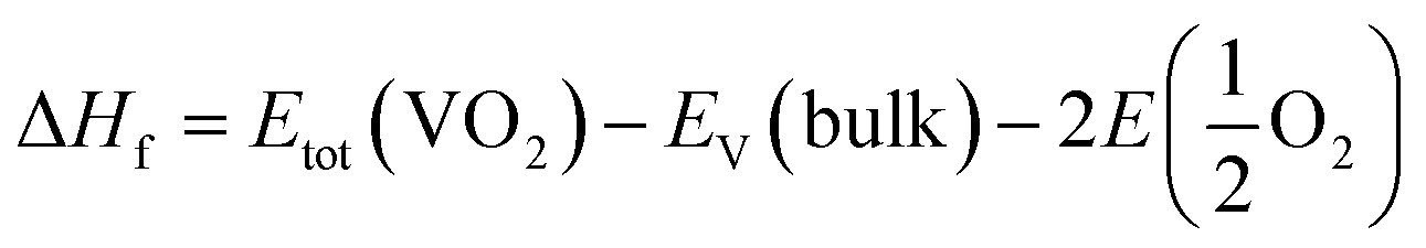 | (1) |
 is the total energy of the oxygen molecules.
The phase transition temperature (Tc) can be quantitatively calculated via30
 | (2) |
As shown in Fig. 1(a and b), the basic calculations were performed in the supercells with 2 × 2 × 2 and 2 × 2 × 4 primitive unit cells for VO2(M) and VO2(R) phases, respectively. Table 1 lists the calculated structural parameters. The theoretical lattice parameters obtained in this work are in good agreement with the previously reported experimental data.31
 | ||
| Fig. 1 Crystalline structures of monoclinic (a) and rutile (b) phases of VO2. V and O atoms are represented by gray and red spheres, respectively. | ||
3. Results and discussion
3.1 Charge induced phase transition for VO2
Fig. 2(a and b) shows the total energies (Etot) of charge doping in M and R phase as a function of charge density. It can be found that the total energies of charge-doping M phase VO2 are gradually lower than those of R phase as the charge doping increases, indicating that it is more difficult to obtain R phase VO2 than the M phase under current conditions. The similar results have been also appeared in electron-injection in two-dimensional transition metal dichalcogenides.32 Fig. 2(c and d) shows the formation enthalpy of charge-doped VO2. The trend of the formation enthalpy of electron doping and that of hole doping are contrary. The formation enthalpy of VO2 linearly increased with the increase in electron density, while the formation enthalpy of VO2 decreased with the increase in hole density. In addition, hole doping system is more negative than the pristine one, and the electron doping system is less negative than the pristine one, suggesting that hole doping system is more stable than the electron doping. Thus, we conclude that hole doping is more conducive to stabilize the structure of VO2 than electron doping. This phenomenon has been found in IIA element doping of VO2(M).9 Zhang et al. reported that the introduction of some electrons in VO2 via W doping results in the instability of the structure.22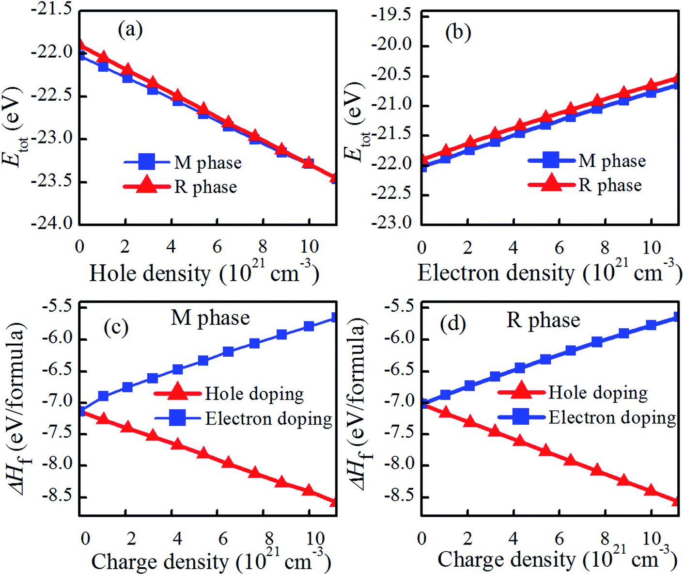 | ||
| Fig. 2 Total energies (Etot) of charge doping in M and R phase as a function of charge density, and formation energy of charge doped VO2. (a) Hole doping, (b) electron doping, (c) charge doped VO2(M), and (d) charge doped VO2(R). | ||
The dependence of Tc on the charge doping concentration is presented in Fig. 3(a and b). As shown in Fig. 3(a), the Tc of VO2 is found to be almost linearly proportional to the hole-doping density. It is clearly shown that when the hole density is set at 4.28 × 1021 cm−3, the phase transition of VO2 could take place at 162.44 K, which is lower than the room temperature of 298 K. This observation is consistent with the experimental observation that hole doping could trigger the MIT below 340 K.17 Wan et al. reported that the reduced phase transition temperature for hole doped VO2 is due to the fact that hole doping modifies the V-3d orbital occupancy and thus weakens the electron–electron correlation, lowering the crystalline stability energy.17 Dai et al. found that F-doping can effectively decrease the Tc to 35 °C at 2.93% F in VO2 and that F-doping VO2 smart glass foils exhibit excellent thermochromism in the near-infrared region.19 However, the situation for electron-doping is not the same as that of hole-doping. As shown in Fig. 3(b), when the electron density increases from 0 to 2.1 × 1021 cm−3, Tc gradually increases. However, once the electron density is greater than 2.1 × 1021 cm−3, Tc rapidly decreases. For example, an electron density of 2.1 × 1021 cm−3 corresponds to a ΔTc of 11.72 K for electron-doped VO2, i.e., the phase transition from the rutile phase to the monoclinic phase occurs at 351.72 K. However, an electron density of 1.12 × 1022 cm−3 will result in a ΔTc as large as −25.32 K, implying the reduction in Tc to 314.68 K. Actually, the Tc is related with the charge concentration. In the range of charge concentration, the Tc is almost linearly proportional to the charge density. Experimentally, when cooled down to 120 K, HxVO2 (x > 4%) films exhibit metallic properties, and the ΔTc was around −55 K per at% H.23
 | ||
| Fig. 3 Dependence of the phase transition temperature (Tc) in VO2 on the charge density. (a) Hole-doping, and (b) electron doping. | ||
3.2 Atomic and electronic structures of charge-doped VO2
The reduction in Tc for charge-doped VO2 should be coupled with the changes in the atomic and electronic structure, as discussed in the next section. For charge-doped VO2(M), as shown in Fig. 4(a and b), the lattice parameters b and c of are slightly increase, and the lattice parameter a remains nearly unchanged under the considered electron density. However, these parameters (a, b, c) slightly decrease with increasing of hole density. This outcome further confirms that the reduction in the Tc in hole doped VO2 is due to the shorter a-axis length.33,34 Moreover, the lattice parameter a expressing the V–V chains promotes the transition from the monoclinic phase to the rutile phase at a lower temperature than that of pristine VO2. Applying the compression strain along the a-axis balances the V–V distance. In addition, applying the compression strain along the a-axis results in the overlapping of d orbitals, which increases the d bandwidth and then forces it to transition from the monoclinic phase to the rutile phase, thus causing the reduction in Tc. Experimentally, Fan et al. reported that stretching of a-axis will increase the Tc of VO2 films.33 Muraoka et al. found that the appearance strain along the a-axis from VO2/TiO2 thin films has a large influence on the MIT of VO2.34 Therefore, hole doping in the concentration range considered is able to promote the phase transition in VO2. The opposite is true for electron doping. For charge-doped VO2(R), as shown in Fig. 4(c and d), the c axis is slightly shorten, and then slightly elongated in the hole-doping VO2(R), while the c axis is slightly elongated in electron-doping VO2(R). This may attribute the fact that the charge-injection would induce variable orbital occupancy, which is similar to the experimental results.19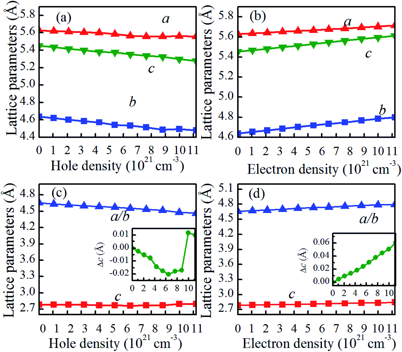 | ||
| Fig. 4 Lattice parameters of (a) hole or (b) electron doped VO2(M), and (c) hole or (d) electron doped VO2(R). The inset figure is the variation of c, i.e., Δc (c − c0). The c and c0 are the supercell lengths along the c-axis at equilibrium and charge-doped VO2. | ||
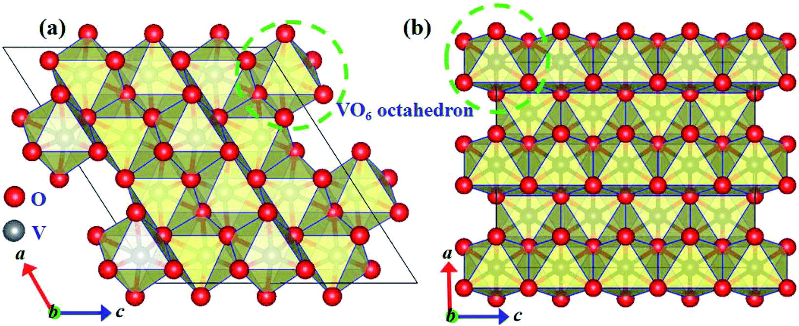
It is reported that the V–V chains are one of the key characteristics of VO2 in determining the atomic and electronic properties at different phases.35,36 As shown in Fig. 1, in pristine VO2(R), all the V atoms arrange uniformly along the c axis with nearest-neighbor V–V distances of 2.788 Å. However, pristine VO2(M) exhibits Peierls distortion in the V–V chains along the a-axis, in which the short and long V–V bonds (2.520 Å vs. 3.143 Å) are arranged alternately. Compared with those of pristine VO2(M), as shown in Fig. 5(a and b), the short and long V–V bond distances are nearly unchanged and still maintain the dimerization characteristics after electron doping. However, hole doping results in a gradual shortening of the long V–V bond distances and a gradual elongation of the short V–V bond distances below a critical hole density of 6.48 × 1021 cm−3. This phenomenon could also be observed experimentally in the intermediate phase of VO2(M2), in which only half of the V atoms are dimerized, while the other half form chains of is equally spaced atoms.37 Once above the critical hole density, the alternatively short and long V–V bond distances jump, and the equidistant V–V bond distances (2.7–2.8 Å) are similar to the V–V bond length in VO2(R) (as shown in Fig. 5(a)). These results indicate that VO2 transits from the monoclinic phase to the rutile phase within the range of a certain hole-doping density. Yuan et al. proved that the appearance of this phenomenon is attributed to a strong lattice-hole coupling.38 Experimentally, it is found that a critical hole density induces a sudden rapidly variable V–V bond, which is related to the critical excitation influence.39–42 As shown in Fig. 5(c), the V–V distances in the hole-doping VO2(R) has a very fast change into alternatively short and long bond distances, for the V–V chains. In contrast, as shown in Fig. 5(d), the V–V distances in electron-doping VO2(R) seem slightly to increase. Therefore, it can be concluded that the hole-injection has greater influence on the V–V bond lengths than the electron-injection in VO2.
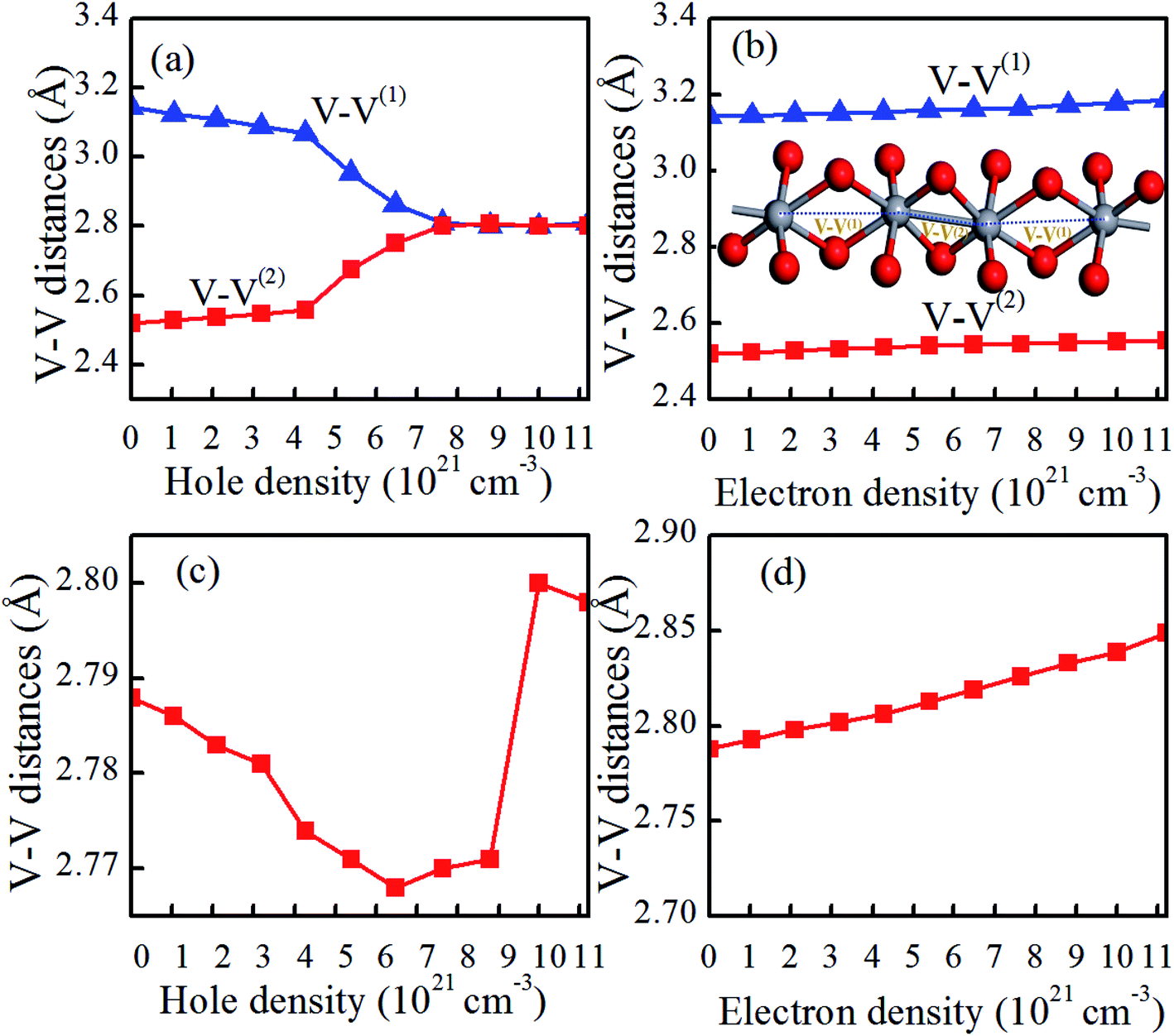 | ||
| Fig. 5 Dependence of V–V distances in (a) hole or (b) electron doped VO2(M) and (c) hole or (d) electron doped VO2(R) on the charge-doping density. The long V–V bonds denote V–V(1), and the short V–V bonds denote V–V(2). The inserted figure shows the V–V bonds in the VO2(M). The V and O atoms are indicated by the gray and red spheres, respectively. | ||
The structural transition in VO2 is accompanied by changes in the electronic band structure near the Fermi level that can be qualitatively understood within a crystal field model.31 As shown in Fig. 6(a), the twisting of the V–V chains causes splitting of the d‖ orbital into filled bonding and empty antibonding orbitals, while making the π* orbital move to a higher energy level, thus opening the band gap. Actually, the VO2 phase transition is relative to the octahedral environment and the associated hybridization of the O-2p orbitals with the V-3d orbital.31 As shown in Fig. 6(b), for VO2(M), each VO6 octahedron shares edges with its neighboring octahedra, forming chains along the a-axis. In addition, the V-3d orbitals split into a combination of low-energy states and high-energy states, where the high-energy states involve the symmetry of the V–O bonds. In charge-doping VO2(M), as shown in Fig. 6(c and d), the V–O distance is slightly lengthened with the increase in electron density, and could further decrease the p–d overlap.43 The increase in the V–O bond results in the expansion of the lattice volume due to the decrease in cR/aR and further induces the reduction in Tc.43 Therefore, we can conclude that electron doing makes the V–O bond length longer and thus reduces the Tc in VO2. However, as the hole density increases, the V–O bond lengths are gradually reduced. When the hole density reaches 5 × 1021 cm−3, d2 experiences a dramatic increase, and d5 decreases sharply, which will increase the p–d overlap, and thus both the d‖ and π* orbitals are partially occupied at Fermi level.43 This phenomenon confirms that VO2 may experience a metal–insulator transition.
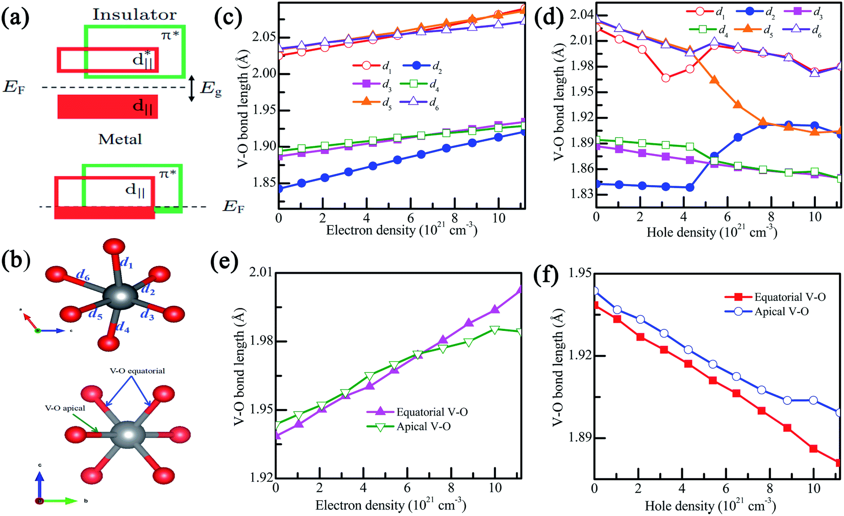 | ||
| Fig. 6 (a) Bandwidth scheme of pristine VO2, (b) an octahedron at the center of VO2, (c and d) the V–O bond lengths in charge doped VO2(M), and (e and f) the V–O bond lengths in hole-doped VO2(R). The bond distances in VO2(M) are d1, d2, d3, d4, d5 and d6. The bond lengths in VO2(R) are the equatorial and apical V–O. | ||
As shown in Fig. 6(e), in the VO2(R), the apical and equatorial V–O bond lengths increase with the increase of electron density, which is due to the decrease in the ration of c/a. However, as shown in Fig. 6(f), the apical and equatorial V–O bond lengths decrease with the increase hole density.
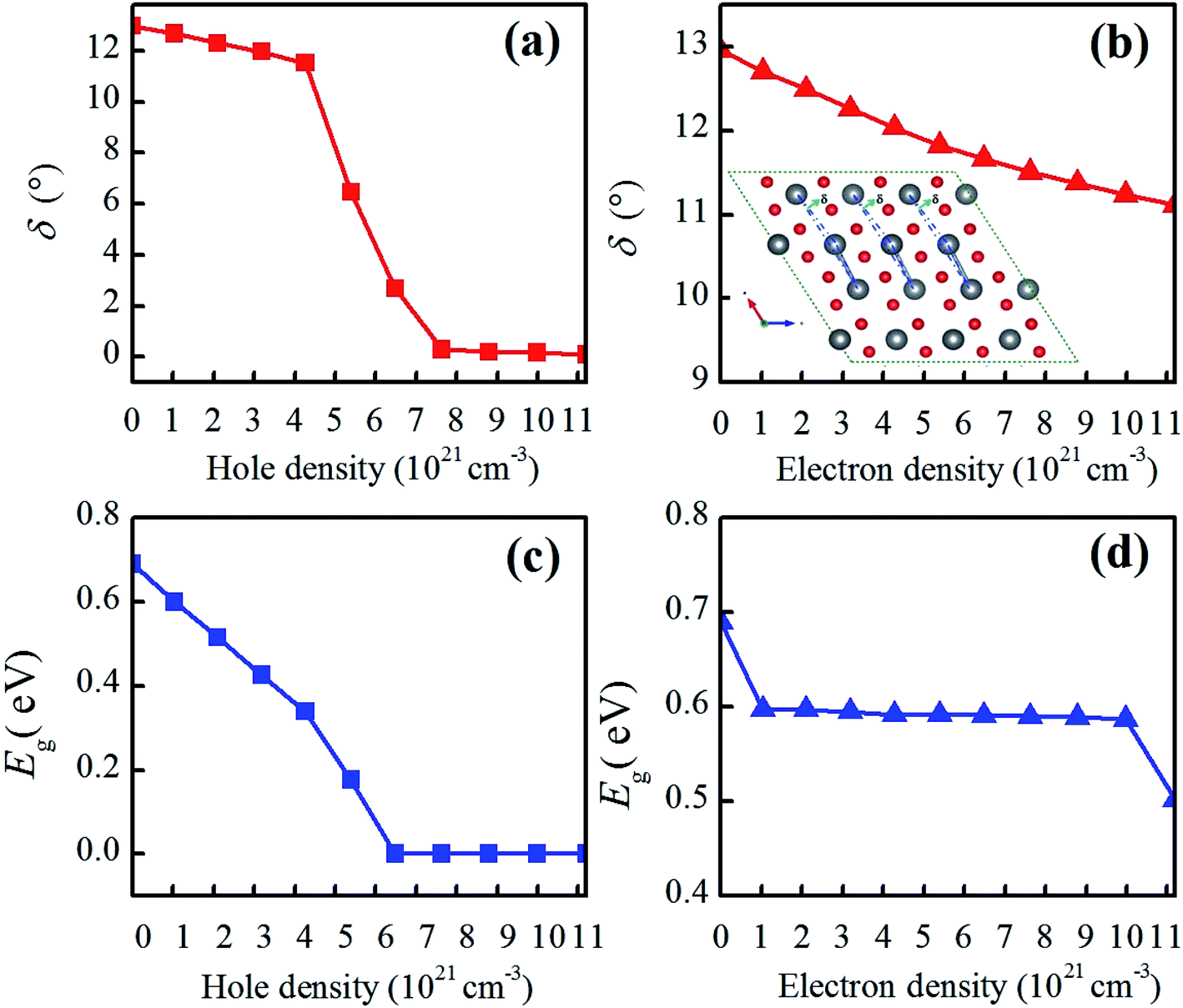
Except for the variable V–O bond, the band gap evolution of charge-doped VO2 is related to the atomic structure change described by the V–V chains and twisting angle δ and the electronic structure change described by orbital switching. As shown in Fig. 7(a and b), δ in the V–V chains of electron-doped VO2 tends to gradually decrease, indicating that the V–V bond characterizes a dimerizing feature. However, when the hole density is from 0 to 4.28 × 1021 cm−3, δ in the V–V chains decreases monotonically, as the hole density increase further, the value of δ sharply decreases, finally reaching zero, which demonstrates that the alternatively short and long V–V bond distances in VO2(M) quickly change into equal V–V bonds. In addition, the average twisting angle δ in the V–V chains exhibits excellent consistency with the band gap change of VO2 from R to M1. As in Gao's previous discussion,35 the significant dimerization in V–V, slight twisting of δ or the variable V–O bond can be regarded as the characteristic parameters of the structure-driven transition. As shown in Fig. 7(c), when the hole density is increased by 5.4 × 1021 cm−3, the band gaps of VO2(M) linearly decrease and eventually decrease to 0 eV with the increase in hole density. The band gap undergoes a fast change, and exhibits a similar change tendency as the twisting angle δ. This phenomenon is consistent with the other result calculated from Lee et al.,14 who reported that VO2 exhibits a significant band-gap narrowing for a charge concentration from 0.025 to 0.5 hole/electron per VO2. Experimentally, Zhang et al. found that N atoms-substituted O atoms induce narrowing of the energy band gap due to weakening of the interaction within the V–V dimer with the hole injected into the d‖ sub-bands.18 In contrast, as shown in Fig. 7(d), as the electron density increases from 0 to 1.2 × 1022 cm−3, the band gaps of VO2(M) experience a slight reduction ranging from 0.69 eV to 0.502 eV. Apparently, electron doping induces a slow MIT, and its density has some effect on the phase transition. Theoretically, a fascinating rebound behavior of the transition temperature is observed. By increasing the doping concentration of W into VO2, the MIT is tuned to a lower temperature at the beginning and then anomalously shifted to a higher temperature.44
 | ||
| Fig. 7 (a and b) Average twisting angle (δ) of the V–V chains and (c and d) the band gaps in charge-doped VO2(M). (a and c) Electron doping, and (b and d) hole doping. The inserted figure in (b) is the δ angle in the V–V chains in VO2(M). | ||
In order to reveal the kinetic limit for charge-driven phase transition in VO2, we performed CINEB calculations to obtain the phase transition barriers. As shown in Fig. 8(a), we redefined the lattice parameters for VO2(R) from tetragonal and monoclinic view to better reveal the kinetic limit for charge-driven phase transition in VO2 (As listed in Table 2). Fig. 8(b) shows the energy curves of M-to-R phase transition in pristine and charge-doping VO2 with certain density. It can be found that the energy barriers are too higher for VO2 transiting from M phase to R phase, indicating that it requires additional conditions to drives the M-to-R phase transition, such as the temperature, pressure and light radiation.32
 | ||
| Fig. 8 (a) Structures of VO2 (M/R) and (b) energy barriers from M to R phase under different charge doping. | ||
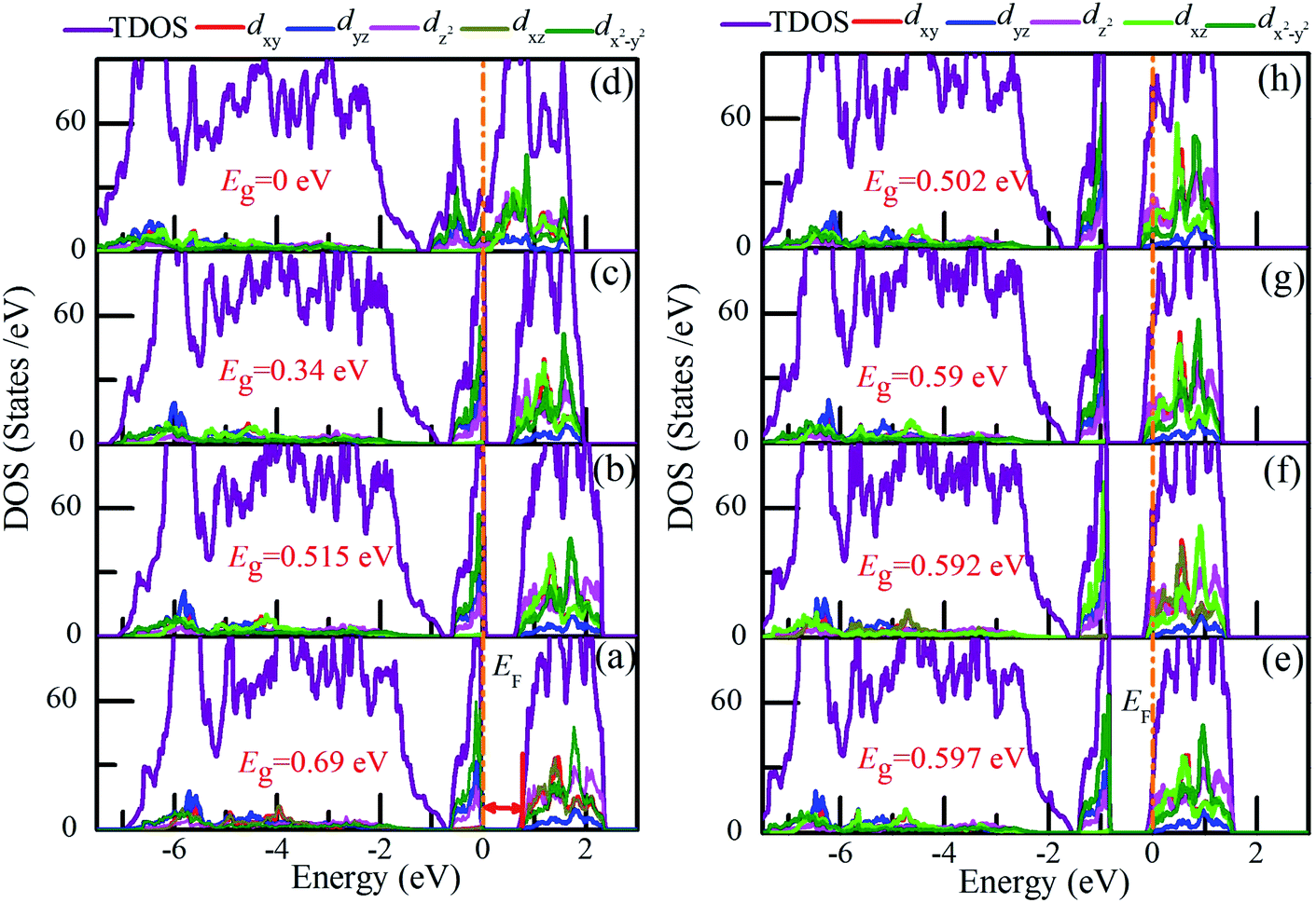
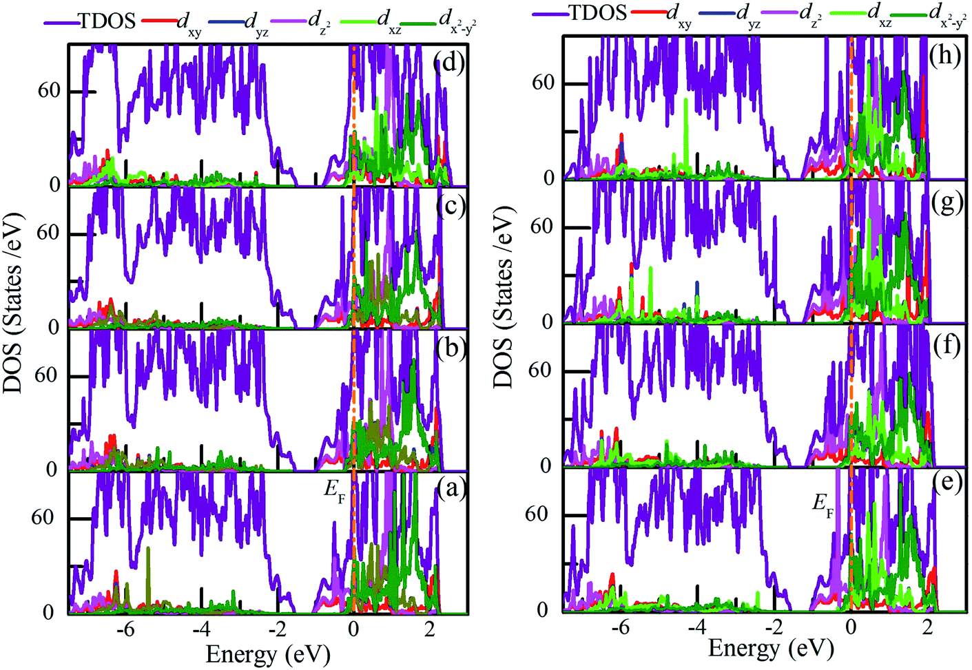
To elucidate the possible driving forces behind the MIT, we further calculated the total and partial densities of states (DOSs) of charge-doped VO2(M). As shown in Fig. 9(a), for pristine VO2(M), the electrons around EF occupy the t2g-state dx2−y2 orbital (π), while the conduction is mainly occupied by the eg-state dz2 orbital (σ). At hole densities of 2.1 × 1021 cm−3 and 4.28 × 1021 cm−3, the band gaps of VO2(M) are reduced to 0.515 eV and 0.34 eV, respectively. Near the EF, the electrons dominantly occupy the dx2−y2 orbital and dyz orbital. In contrast, fewer electrons occupy the dz2 orbital (σ). More importantly, this electronic structure characteristic remains from 0 to 6.48 × 1021 cm−3 (the critical hole density). Interestingly, when the hole density reaches the critical hole density, VO2 exhibits metallic properties, as shown in Fig. 9(d). There is a strong interaction near the Fermi level between the dx2−y2 and dz2 orbitals. This result is also consistent with the previous discussion on the significant dimerization in V–V and a slight twisting of δ, which could be regarded as the characteristic parameters of the structure-driven transition. However, from Fig. 9(e–h), the Fermi levels are shifted into the conduction band to varying degrees with the increase in electron doping. The states near the Fermi level are mainly occupied by the dz2 orbital, while the valence bands mainly consist of the dx2−y2 orbital. Furthermore, it can be observed that the electronic structure of VO2 changes slightly for different electron concentrations. More importantly, although there are some changes in the band gap from 0.597 eV to 0.502 eV and the location of EF, this electronic structure characteristic remains as electron doping increases. Therefore, it can be concluded that the band gap of VO2 with charge doping should be attributed to an electron-correction-driven Mott transition in which orbital switching occurs between the dx2−y2 and dz2 states. Experimentally, by soft-X-ray absorption spectroscopy, orbital-assisted MIT is also observed in VO2.43
 | ||
| Fig. 9 Total and projected density of states (DOS) of (b–d) hole-doped and (e–h) electron-doped VO2(M). The concentrations of charge are (a) pristine, (b) 2.1 × 1021 cm−3, (c) 4.28 × 1021 cm−3, (d) 8.8 × 1021 cm−3, (e) 1.04 × 1021 cm−3, (f) 4.28 × 1021 cm−3, (g) 7.63 × 1021 cm−3, and (h) 1.12 × 1022 cm−3. The Fermi level (EF) is set to 0 eV. | ||
Fig. 10 shows the density of states of pure VO2(R) and charge-doping VO2(R). It is seen that pristine VO2(R) and charge-doped VO2(R) exhibit metallic properties as the Fermi level crosses the conduction band. Furthermore, electrons around Fermi level mainly occupy the dx2−y2 orbital and dz2 orbital. In addition, as the hole density increases, the former has a higher occupant than the latter. However, as the electron density increases, the occupant of dz2 orbital is higher than that of the dx2−y2 orbital. In general, there is a significant orbital switching between the dx2−y2 and dz2 orbitals accompanied by obvious V–V dimerization and a slight twisting of δ in the charge-doped VO2.
 | ||
| Fig. 10 Total and projected density of states (DOS) of (b–d) hole-doped and (e–h) electron-doped VO2(R). The concentrations of charge are (a) pristine, (b) 2.1 × 1021 cm−3, (c) 4.28 × 1021 cm−3, (d) 8.8 × 1021 cm−3, (e) 1.04 × 1021 cm−3, (f) 4.28 × 1021 cm−3, (g) 7.63 × 1021 cm−3, and (h) 1.12 × 1022 cm−3. The Fermi level (EF) is set to 0 eV. | ||
3.3 Discussion
Charge-doping greatly impacts on the atomic and electronic structures of VO2. From the Fig. 3, it is found that the charge-doping including hole and electron-doping could trigger the phase transition of VO2. More interestingly, the effect of hole doping on the Tc is greater than that of electron-doping. This is consistent with other calculation result. As is predicted by Zhang et al., the hole doping was superior to electron doping for modulating the phase transition of VO2.38 From a geometric viewpoint, the octahedra in VO2 are orthorhombically distorted, making it possible to differentiate the V–O bonds. After electron-doping, the V–O bond length change significantly in VO2(R). However, for hole-doping, the alternatively short and long V–V bond distances has very fast change into the equidistant V–V bond in VO2(M). Furthermore, the twisting angle δ experiences a great change. These phenomena are ascribed to structure-driven transition due to the large δ and V–V bond length change.35 From the electronic structure viewpoint, the characteristic of VO2 transition from the semiconducting state to the metallic state appears due to the strong interaction between the dx2−y2 and dz2 orbitals near the Fermi level, which can be attributed to the electron-driven the transition. Therefore, it can be concluded that charge-doping may provide an efficient way to modulate the MIT in VO2.4. Conclusions
In summary, we performed first-principles calculations to investigate the behavior of charge doping and its influence on the phase transition temperature of VO2. Charge doping could effectively modulate the Tc, assisting the VO2 phase transition at room temperature. Hole doping induces a significant band-gap narrowing with increasing of hole concentration. The characteristic VO2 transition from the semiconducting state to the metallic state appears once above the critical hole density (6.48 × 1021 cm−3), which is due to the strong interaction between the dx2−y2 and dz2 orbitals near the Fermi level. However, electron doping shows a slight band-gap narrowing with increasing electron concentration. The V–O bond lengths significantly increase. The results will provide insights into phase transitions of VO2 thermochromic materials across the MIT suitable for applications such as smart windows.Conflicts of interest
There are no conflicts to declare.Acknowledgements
The authors gratefully acknowledge support from the National Natural Science Foundation of China (51873102, 51972206), the Open Project Fund of Key Laboratory for Optoelectronics and Communication of Jiangxi Province (20181OEC001), the School-level Scientific Research Project of Hubei Polytechnic University (18xjz11R), and the Innovation Training Program of Hubei Province (S201910920031). The computation was conducted using the high performance computing platform of Shanghai University.References
- F. J. Morin, Phys. Rev. Lett., 1959, 3, 34–36 CrossRef CAS.
- C. Granqvist, Phys. Scr., 1985, 32, 401–407 CrossRef CAS.
- T. Driscoll, H. Kim, B. Chae, M. Ventra and D. Basov, Appl. Phys. Lett., 2009, 95, 043503 CrossRef.
- B. Kim, Y. Lee, B. Chae, S. Yun, S. Oh, H. Kim and Y. Lim, Appl. Phys. Lett., 2007, 90, 023515 CrossRef.
- L. Kang, Y. Gao, H. Luo, J. Wang, B. Zhu, Z. Zhang, J. Du, M. Kanehira and Y. Zhang, Sol. Energy Mater. Sol. Cells, 2011, 95, 3189–3194 CrossRef CAS.
- Y. Gao, S. Wang, H. Luo, L. Dai, C. Cao, Y. Liu, Z. Chen and M. Kanehira, Energy Environ. Sci., 2012, 5, 6104–6110 RSC.
- Y. Cui, Y. Ke, C. Liu, Z. Chen, N. Wang, L. Zhang, Y. Zhou, S. Wang, Y. Gao and Y. Long, Joule, 2018, 2, 1707–1746 CrossRef CAS.
- C. Tang, P. Georgopoulos, M. E. Fine, J. B. Cohen, M. Nygren, G. S. Knapp and A. Aldred, Phys. Rev. B: Condens. Matter Mater. Phys., 1985, 31, 1000–1011 CrossRef CAS PubMed.
- L. Chen, Y. Liu, K. Yang, P. Lan, Y. Cui, H. Luo, B. Liu and Y. Gao, Comput. Mater. Sci., 2019, 161, 415–421 CrossRef CAS.
- L. Chen, Y. Cui, S. Shi, B. Liu, H. Luo and Y. Gao, RSC Adv., 2016, 6, 86872 RSC.
- S. Zhang, I. S. Kim and L. J. Lauhon, Nano Lett., 2011, 11, 1443–1447 CrossRef CAS PubMed.
- J. P. Pouget, H. Launois, J. P. D'haenens, P. Merenda and T. M. Rice, Phys. Rev. Lett., 1975, 35, 873–875 CrossRef CAS.
- J. Jeong, N. Aetukuri, T. Graf, T. D. Schladt, M. G. Samant and S. S. P. Parkin, Science, 2013, 339, 1402–1405 CrossRef CAS PubMed.
- D. Lee, B. Chung, Y. Shi, G. Y. Kim, N. Campbell, F. Xue, K. Song, S. Choi, J. Podkaminer, T. Kim, P. Ryan, J. Kim, T. Paudel, J. Kang, J. Spinuzzi, D. Tenne, E. Tsymbal, M. Rzchowski, L. Chen, J. Lee and C. Eom, Science, 2018, 362, 1037 CrossRef CAS PubMed.
- J. Zhang, H. He, Y. Xie and B. Pan, Phys. Chem. Chem. Phys., 2013, 15, 4687 RSC.
- K. Wang, W. Zhang, L. Liu, P. Guo, Y. Yao, C. Wang, C. Zou, Y. Yang, G. Zhang and F. Xu, Appl. Surf. Sci., 2018, 447, 347–354 CrossRef CAS.
- M. Wan, M. Xiong, N. Li, B. Liu, S. Wang, W. Ching and X. Zhao, Appl. Surf. Sci., 2017, 410, 363–372 CrossRef CAS.
- W. Zhang, K. Wang, L. Fan, L. Liu, P. Guo, C. Zou, J. Wang, H. Qian, K. Ibrahim, W. Yan, F. Xu and Z. Wu, J. Phys. Chem. C, 2014, 118, 12837–12844 CrossRef CAS.
- L. Dai, S. Chen, J. Liu, Y. Gao, J. Zhou, Z. Chen, C. Cao, H. Luo and M. Kanehira, Phys. Chem. Chem. Phys., 2013, 15, 11723–11729 RSC.
- M. Wan, B. Liu, S. Wang, L. Hu, H. Tao and X. Zhao, J. Alloys Compd., 2017, 706, 289–296 CrossRef CAS.
- T. Hajlaoui, N. Émond, C. Quirouette, B. L. Drogoff, J. Margot and M. Chaker, Scr. Mater., 2020, 177, 32–37 CrossRef CAS.
- J. Zhang, H. He, Y. Xie and B. Pan, J. Chem. Phys., 2013, 138, 114705 CrossRef PubMed.
- V. Andreev, V. M. Kapralova and V. Klimov, Phys. Solid State, 2007, 49, 2318–2322 CrossRef CAS.
- G. Kresse and J. Hafner, Phys. Rev. B: Condens. Matter Mater. Phys., 1993, 47, 558–561 CrossRef CAS PubMed.
- G. Kresse and J. Furthmuller, Phys. Rev. B: Condens. Matter Mater. Phys., 1996, 54, 11169–11186 CrossRef CAS PubMed.
- J. P. Perdew, K. Burke and M. Ernzerhof, Phys. Rev. Lett., 1996, 77, 3865–3868 CrossRef CAS PubMed.
- P. E. Blochl, Phys. Rev. B: Condens. Matter Mater. Phys., 1994, 50, 17953–17979 CrossRef PubMed.
- S. L. Dudarev, G. A. Botton, S. Y. Savrasov, C. J. Humphreys and A. P. Sutton, Phys. Rev. B: Condens. Matter Mater. Phys., 1998, 57, 1505–1509 CrossRef CAS.
- L. Chen, A. Wang, Z. Xiong, S. Shi and Y. Gao, Appl. Surf. Sci., 2019, 467–468, 22–29 CrossRef CAS.
- M. Netsianda, P. E. Ngoepe, C. Richard, A. Catlow and S. M. Woodley, Chem. Mater., 2008, 20, 1764–1772 CrossRef CAS.
- J. Goodenough, J. Solid State Chem., 1971, 3, 490–500 CrossRef CAS.
- X. Zhou, H. Shu, Q. Li, P. Liang, D. Cao and X. Chen, J. Mater. Chem. C, 2020, 8, 4432–4440 RSC.
- L. Fan, S. Chen, G. Liao, Y. Chen, H. Ren and C. Zou, J. Phys.: Condens. Matter, 2016, 28, 255002 CrossRef CAS PubMed.
- Y. Muraoka, Y. Ueda and Z. Hiroi, J. Phys. Chem. Solids, 2002, 63, 965–967 CrossRef CAS.
- S. Chen, J. Liu, H. Luo and Y. Gao, J. Phys. Chem. Lett., 2015, 6, 3650–3656 CrossRef CAS PubMed.
- T. Yao, X. Zhang, Z. Sun, S. Liu, Y. Huang, Y. Xie, C. Wu, X. Yuan, W. Zhang, Z. Wu, G. Pan, F. Hu, L. Wu, Q. Liu and S. Wei, Phys. Rev. Lett., 2010, 105, 226405 CrossRef PubMed.
- Y. Ji, Y. Zhang, M. Gao, Z. Yuan, Y. Xia, C. Jin, B. Tao, C. Chen, Q. Jia and Y. Lin, Sci. Rep., 2014, 4, 4854 CrossRef CAS PubMed.
- X. Yuan, W. Zhang and P. Zhang, Phys. Rev. B: Condens. Matter Mater. Phys., 2013, 88, 035119 CrossRef.
- C. Kübler, H. Ehrke, R. Huber, R. Lopez, A. Halabica, R. F. Haglund and A. Leitenstorfer, Phys. Rev. Lett., 2007, 99, 116401 CrossRef PubMed.
- P. Baum, D. S. Yang and A. H. Zewail, Science, 2007, 318, 788 CrossRef CAS PubMed.
- S. Wall, D. Wegkamp, L. Foglia, K. Appavoo, J. Nag, R. F. Haglund, J. Stähler and M. Wolf, Nat. Commun., 2012, 3, 721 CrossRef CAS PubMed.
- D. Hilton, R. Prasankumar, S. Fourmaux, A. Cavalleri, D. Brassard, M. Khakani, J. Kieffer, A. Taylor and R. Averitt, Phys. Rev. Lett., 2007, 99, 226401 CrossRef CAS PubMed.
- N. Aetukuri, A. Gray, M. Drouard, M. Cossale, L. Gao, A. Reid, R. Kukreja, H. Ohladag, C. Jenkins, E. Arenholz, K. Roche, H. Dürr, M. Samant and S. Parkin, Nat. Phys., 2013, 9, 661–666 Search PubMed.
- M. Nisar, Z. Lin, G. Xu, Y. Liu and G. Han, J. Appl. Phys., 2019, 126, 195106 CrossRef.
| This journal is © The Royal Society of Chemistry 2020 |