
 Open Access Article
 This Open Access Article is licensed under a Creative Commons Attribution-Non Commercial 3.0 Unported Licence
Device performance limits and negative capacitance of monolayer GeSe and GeTe tunneling field effect transistors†
Peipei Xua,
Jiakun Lianga,
Hong Li *a,
Fengbin Liua,
Jun Tiea,
Zhiwei Jiaoa,
Jing Luod and
Jing Lu*bc
*a,
Fengbin Liua,
Jun Tiea,
Zhiwei Jiaoa,
Jing Luod and
Jing Lu*bc
aCollege of Mechanical and Material Engineering, North China University of Technology, Beijing 100144, P. R. China. E-mail: lihong@ncut.edu.cn
bState Key Laboratory of Mesoscopic Physics and Department of Physics, Peking University, Beijing 100871, P. R. China. E-mail: jinglu@pku.edu.cn
cCollaborative Innovation Center of Quantum Matter, Beijing 100871, P. R. China
dBeijing Research Institute of Automation for Machinery Industry, Beijing, P. R. China
First published on 22nd April 2020
Abstract
Exploring the device performance limits is meaningful for guiding practical device fabrication. We propose archetype tunneling field effect transistors (TFETs) with negative capacitance (NC) and use the rigorous ab initio quantum transport simulation to explore the device performance limits of the TFETs based on monolayer (ML) GeSe and GeTe along with their NC counterparts. With the ferroelectric dielectric acting as a negative capacitance material, the device performances of both the ML GeSe and GeTe NCTFETs outperform their TFET counterparts, particularly for the on-state current (Ion). Ion of the optimal ML GeSe and GeTe TFETs fulfills the demands of the International Technology Roadmap for Semiconductors (ITRS 2015 version) for low power (LP) and high performance (HP) devices, at the “6/5” node range, while with the aid of 80 nm and 50 nm thickness of ferroelectric SrBi2Nb2O9, both their NC counterparts extend the fulfillments at the “4/3” node range.
Introduction
The successful fabrication of sub-10 nm conventional field effect transistors (FETs) based on 2D MoS2, Si nanowires1 and carbon nanotubes2 encourages continuing research including but not limited to conventional FETs with new materials; figuring out the ideal device performance limits is a vital guide for the real device fabrication. Relative to the conventional FET, tunneling FET (TFET) and negative capacitance FET (NCFET) offer two new mechanisms to create a deeper subthreshold slope (SS) than the Boltzmann limit of 60 mV dec−1. The lowest reported SS is only 3.9 mV dec−1 in the vertical Ge–MoS2 TFET at room temperature,3 and the minimum SS is reported for the MoS2 NCFET with ferroelectric hafnium zirconium oxide (HZO) with the value of 6.07 mV dec−1.4 The combination of the two mechanisms, i.e., NCTFET would give a better device performance than TFET or NCFET. Lee et al.5 found that the gate capacitance of Ge/Si NCTFET is 6–9% higher than that of its TFET counterpart. Liu et al.6 found that double-gate Si TFET having an ultrathin body with a negative capacitance can avoid hysteresis and reduce the SS. To some extent, the device performance of NCTFET would represent the performance limit of a new-mechanism device.ML GeSe and GeTe are emerging semiconductors with puckered honeycomb networks such as black phosphorene (BP). The syntheses of ML GeSe7 and ML GeTe8 by mechanical exfoliation have been demonstrated. In contrast to the instability of BP and low carrier mobility of the transition-metal dichalcogenides (TMDs),9–12 ML GeSe and GeTe possess both air-stability13,14 and high carrier mobility,15–17 which are beneficial for the realization of practical equipment. Moreover, ML GeSe and GeTe have moderate band gaps13,15,18–20 and anisotropic electronic properties,13,15,21 which are very attractive merits for a competitive channel of TFET with a planar homogeneous p–i–n architecture. However, the performance limits of ML GeSe and GeTe based new-mechanistic devices are not known. Due to their superior stability and dramatic electronic properties, it is of vital scientific significance to explore the device performance limits of the ML GeSe and GeTe TFETs and NCTFETs.
In this study, we explore the device performance limits of the ML GeSe and GeTe TFETs, when their physical gate length is Lg = 10 nm with various doping concentrations and supply voltages by the rigorous ab initio quantum transport simulation. For the optimal ML GeTe TFETs, the values of Ion (HP) are even more extensive than those of the optimal ML GeSe TFETs and exceed the ITRS demands for HP devices until Vdd is less than 0.65 V. Moreover, the optimal ML GeSe TFETs still surpass the ITRS demands for the LP logic devices at a Vdd of 0.65 V. Furthermore, we choose four different ferroelectric dielectrics to construct a prototype negative capacitance TFET (NCTFET) to improve the performance of the logic devices. We found that the performance of the optimal ML GeSe and GeTe NCTFETs can increase dramatically and exceed the ITRS demands for both LP and HP logic devices at a lower Vdd of 0.55 V. In addition, lower delay time (τ) and power dissipations (PDP) can be obtained in all the ML GeSe and GeTe TFETs, which are much smaller than those of the ITRS requirements.
Models and computational methods
With the optimal ML GeSe and GeTe structures (see Fig. 1(a)), a double-gated (DG) TFET model with a planar p–i–n architecture is built, as shown in Fig. 2(a), that is, the source region is doped with p-type, the gate region is intrinsic, and the drain region is doped with n-type. The transport mechanism of the carriers is band-to-band tunneling (BTBT) in this p–i–n architecture. The tunneling barrier is formed in the intrinsic region, which can be tuned to switch on and off through the gate voltage. We set the length of the gate region (Lg) to 10 nm and the thickness of the SO2 dielectric layer to 0.56 nm. Various p-/n-type source/drain doping concentrations (NS/ND) are taken to optimize the device leakage currents (Ileak) and on-state currents (Ion). We study the device performances of the selected ML GeSe and GeTe TFETs with optimal NS/ND under a series of the supply voltage (Vdd) of 0.4–0.74 V with regards to the ITRS 2015 version. Here, Vdd is the chosen gate voltage drop, which equals to the source–drain voltage, and the value of Vdd with regards to the year target of the ITRS 2015 version, i.e., Vdd of 0.74, 0.65, 0.55, 0.45, and 0.4 V refers to the technical node range of “11/10”, “6/5”, “4/3”, “3/2.5”, and “2/1.5”, respectively.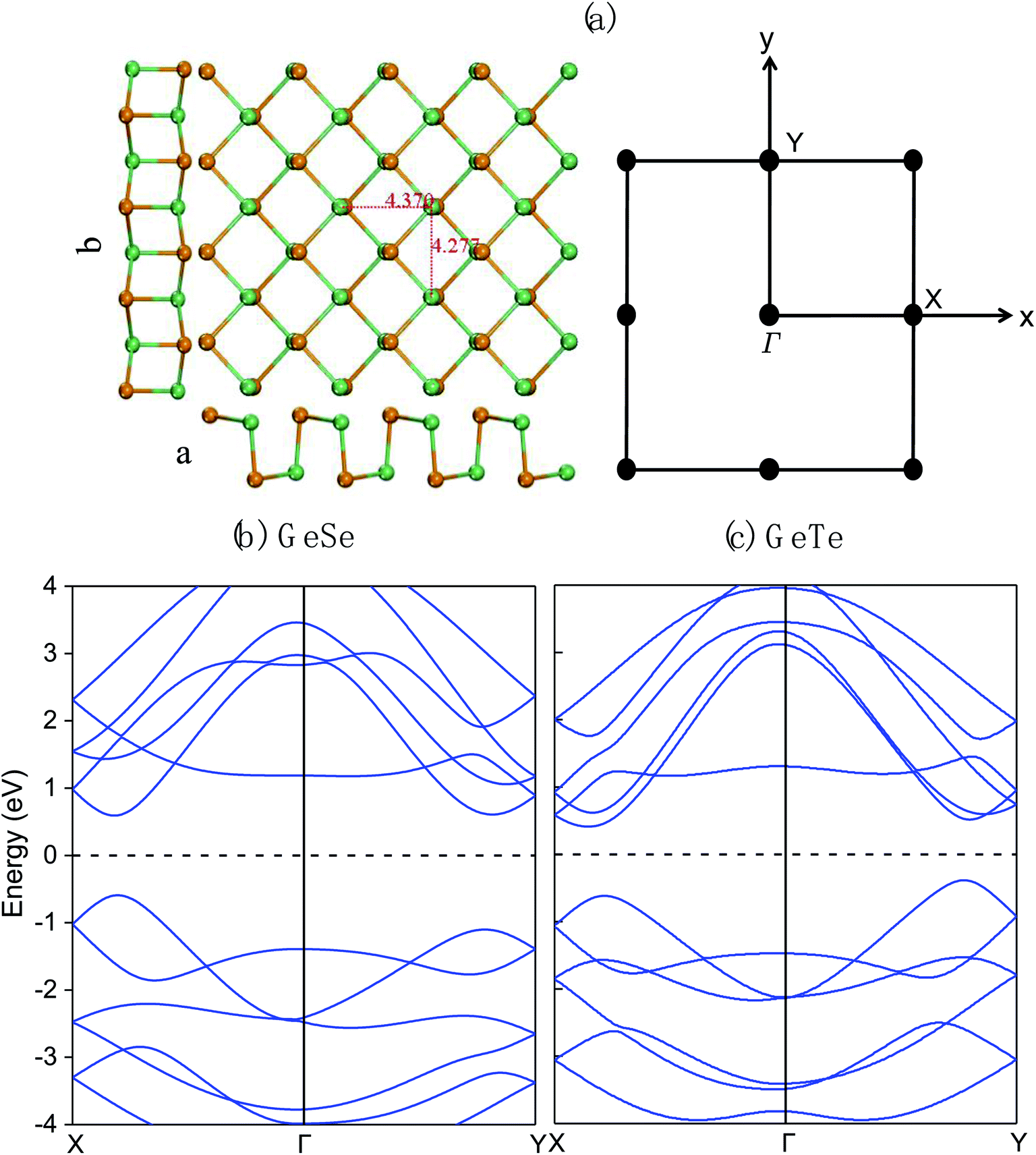 | ||
| Fig. 1 (a) Top and side views of ML GeTe. (b and c) Band structure of the ML GeSe and GeTe. Green ball: Ge atom; brown ball: Te atom. Γ–Y and Γ–X represent the zigzag and armchair directions, respectively. | ||
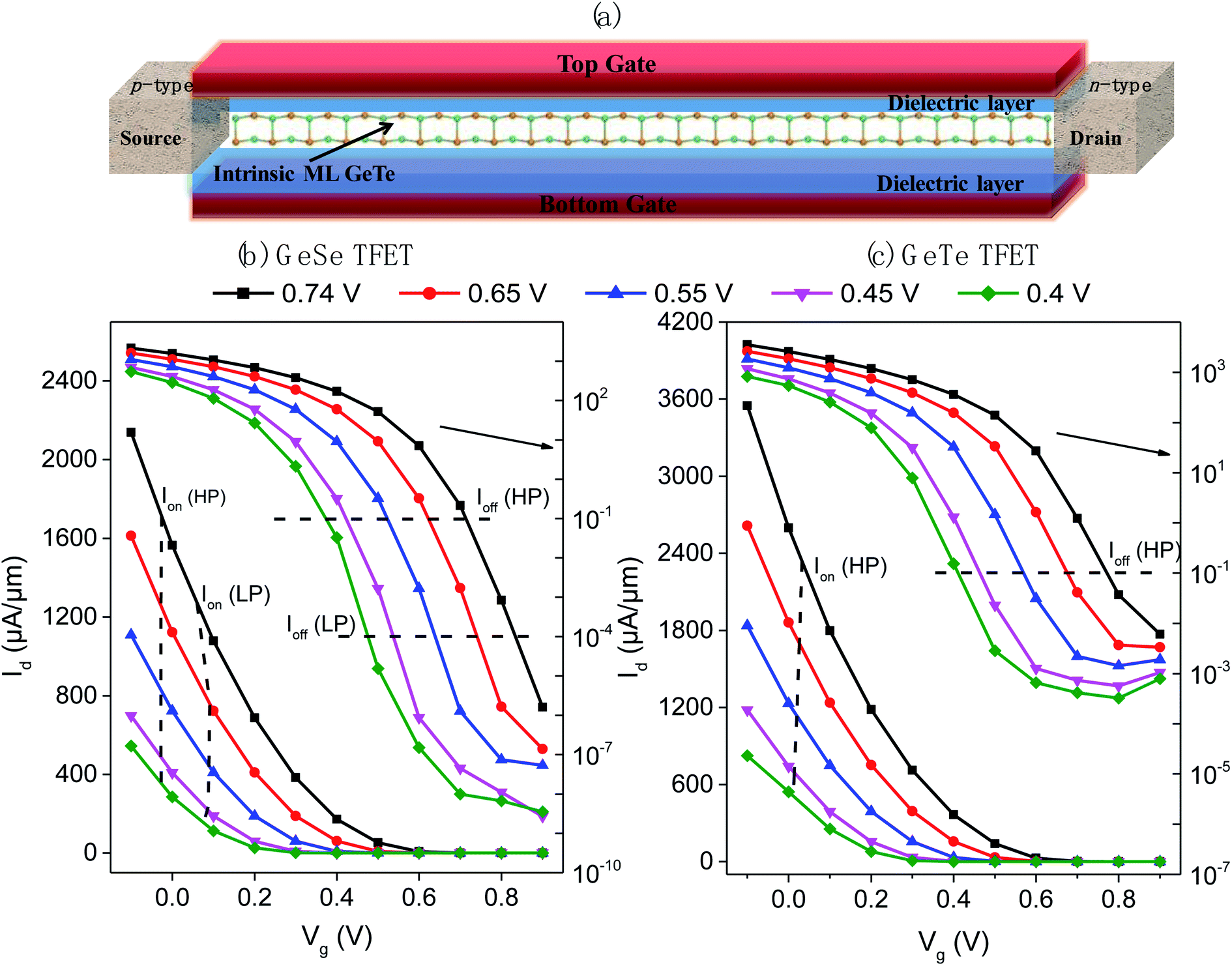 | ||
| Fig. 2 (a) Device model of the ML GeTe TFET. Transfer characteristics of the ML GeSe (b) and GeTe (c) TFETs with Lg = 10 nm at Vdd of 0.4–0.74 V. The ITRS requirements for HP and LP devices (2015 version) are given for comparison. NS/ND is 0.1/5 × 1013 cm−2 for each TFETs. | ||
The electronic property and geometric structures of the ML GeSe and GeTe are investigated using density functional theory (DFT), and the device performances of the ML GeSe and GeTe TFETs are calculated using the non-equilibrium Green's function (NEGF) method based on the DFT, the so-called DFT + NEGF approach. Both the methods are executed in the package of Atomistix Tool Kit (2017 version).22–24 The generalized gradient approximation of Perdew–Burke–Ernzerhof (GGA-PBE) was chosen as the exchange-correlation function.25 The pseudopotential is ‘SG15’ norm-conserving pseudopotential, and the basis set is ‘Medium’. The density mesh cut-off energy and electron temperature are set as 100 Ha and 300 K, respectively. The Monkhorst–Pack k-point sampling26 is 31 × 31 × 1 for 2D crystal calculation and 1 × 31 × 151 k-points for device simulation. The convergence criteria are 10−3 eV Å−1 and 10−5 eV for the maximum force and energy, respectively. The convergence criteria are 10−3 eV Å−1 and 10−5 eV for the maximum force and energy, respectively.
After self-consistent, we calculate the transmission coefficient T(E, ky) using the equation as follows:
| T(E, ky) = Tr[GrΓS(E, ky)GaΓD(E, ky)] |
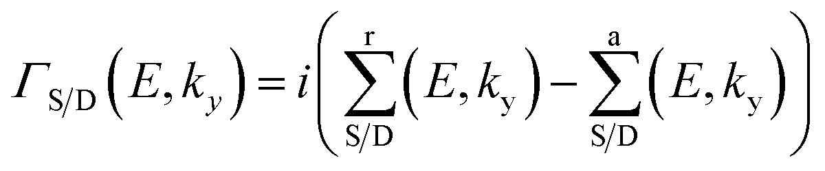 is the line width function expressed in terms of the electrode self-energies
  for the Source and Drain. Then, the average of T(E, ky) over 61 ky-points in the Brillouin zone can be used to obtain the transmission spectrum T(E). The current I(VDS, Vg) can be calculated according to the Landauer–Büttiker formula27 at a given gate voltage Vg and bias voltage VDS by integrating the T(E):
where fS/D is the Fermi–Dirac distribution function, and μS/μD is the electrochemical potential for the Source/Drain. By self-consistently solving the Poisson equations, the gate effect can be realized.
We choose four different ferroelectric capacitors (i.e., BaTiO3, Hf0.5Zr0.5O2 (HZO), PZT, and SrBi2Nb2O9) to construct a negative capacitance TFET (NCTFET) for the ML GeSe and GeTe channels at the Vdd of 0.55 V. With the combination of the Silvaco Atlas commercial simulator and the Landau–Khalatnikov (L–K) theory of ferroelectrics, we can calculate the voltage drop VNC across the ferroelectric film:28,29
| VNC = 2αtFeQ + 4βtFeQ3 + 6γtFeQ5 |
Results and discussion
Geometric and electronic properties
ML GeSe and GeTe have puckered honeycomb networks with orthorhombic crystal structures similar to that of BP. The side and top views of the relaxed puckered atomic configuration of the ML GeTe in the armchair and zigzag directions are shown in Fig. 1(a). The band structures of ML GeSe and GeTe are given in Fig. 1(b) and (c). ML GeSe is a direct gap semiconductor, while ML GeTe is a semiconductor with an indirect bandgap. ML GeSe and GeTe show anisotropic electronic behaviors as the band dispersions along the zigzag (Γ–Y) and armchair (Γ–X) directions are asymmetric. We summarize the optimized lattice parameters, bandgap values, and effective masses in Table 1, with available published results given for comparison. The lattice lengths a/b are 4.27/3.99 Å and 4.37/4.28 Å, for ML GeSe and GeTe, respectively. The value of the bandgap is 1.18 eV for ML GeSe, while the direct/indirect bandgap value of ML GeTe is 0.91/0.80 eV, respectively. The electron/hole effective masses are 0.13/−0.14 and 0.10/−0.12 m0 for ML GeSe and GeTe along the zigzag direction, respectively, which are lighter than those of 0.22/−0.29 and 0.23/−0.17 m0 along the armchair direction. Our calculated lattice lengths, gaps, and electron/hole effective masses are in good agreement with the former calculated and published results for the GeSe and GeTe, as shown in Table 1.14,15Optimal doping concentration
The effect of asymmetric NS/ND is tested at first. From a former study on ML GeSe TFET,34 we find an enhanced p-type character in the device with a lower NS (e.g., NS/ND = 1/5 × 1013 cm−2), while an enhanced n-type character is obtained with an opposite ratio of NS/ND = 5/1 × 1013 cm−2. In this study, we fix ND to 5 × 1013 cm−2, and set NS to 1 × 10¹³, 0.5 × 10¹³ and 0.1 × 1013 cm−2, respectively. For the ML GeSe and GeTe TFETs with Lg = 10 nm, the p-type transfer characteristics along the zigzag direction are presented in Fig. S1(a) and (b) in the ESI.† Ileak values of the ML GeSe TFETs are 8.4 × 10⁻⁴, 6.8 × 10⁻⁵, and 1.6 × 10⁻⁶ μA μm−1 for NS/ND of 1/5 × 1013, 0.5/5 × 1013, and 0.1/5 × 1013 cm−2, respectively, which are more than three orders of magnitude smaller than those of the ML GeTe TFETs (1.41, 0.3, and 6.08 × 10⁻³ μA μm−1) at the same NS/ND.The off-current Ioff (HP)/Ioff (LP) is taken as 0.1 × 10⁻⁴ μA μm−1 from the ITRS demands (2015 version), and the corresponding Vg is marked as Vgoff (HP)/Vgoff (LP). For Vdd = 0.74 V, Ion (HP) is then obtained at Vgon (HP) = Vgoff (HP) − 0.74 V. The value of Ion (HP) of the ML GeSe TFETs increases from 1654, 1664, to 1715 μA μm−1 as NS decreases from 1 × 10¹³, 0.5 × 10¹³ to 0.1 × 1013 cm−2, respectively, with all exceeding the ITRS requirement of 1287 μA μm−1 for HP devices at similar Vdd of 0.75 V. Ion (HP) of 2342 μA μm−1 of the ML GeTe TFET is much larger than those of the ML GeSe TFETs. Ileak values of the ML GeSe TFETs meet Ioff (LP) at NS = 0.5 × 10¹³ and 0.1 × 1013 cm−2, and the corresponding Ion (LP) are 759 and 1272 μA μm−1, which exceed the ITRS requirement of 629 μA μm−1 for the LP devices. In total, the optimal doping concentration is NS/ND = 0.1/5 × 1013 cm−2 for both the GeSe and GeTe TFETs with regards to Ileak and Ion.
Device performance
Herein, we explore the device performance limits of the ML GeSe and GeTe TFETs under the optimal doping concentration of NS/ND = 0.1/5 × 1013 cm−2 with regards to the ITRS demands of HP and LP devices. We plot the enhanced p-type transfer characteristics of the ML GeSe and GeTe TFETs with Lg = 10 nm with different supply voltages (Vdd = 0.4–0.74 V) in Fig. 2(b) and (c) and Ion vs. Ioff (HP/LP) in Fig. 3(a). With the decrease in the supply voltages from 0.65 to 0.4 V, the Ion (HP) values of ML GeSe TFETs decrease from 1200 to 355 μA μm−1, which do not reach the requirements of ITRS (2015 version) for HP devices (see Table 2). Notably, Ion (LP) of the ML GeSe TFET is 759 μA μm−1 (Vdd = 0.65 V), which is 1.2 times of the requirement of 629 μA μm−1 of the ITRS (2015 version) for LP devices. Ion (HP) of the ML GeTe TFET is 1699 μA μm−1 at Vdd of 0.65 V, which prominently exceeds the requirement (i.e., 1476 μA μm−1) of ITRS (2015 version) for the HP device. However, as Vdd decreases to less than 0.65 V, the optimal ML GeTe TFETs can still possess high Ion (HP) of 512–1135 μA μm−1, and Ion (LP) of the optimal ML GeSe TFETs is 156–444 μA μm−1, which all cannot exceed the ITRS (2015 version) demands for the HP and LP devices, respectively.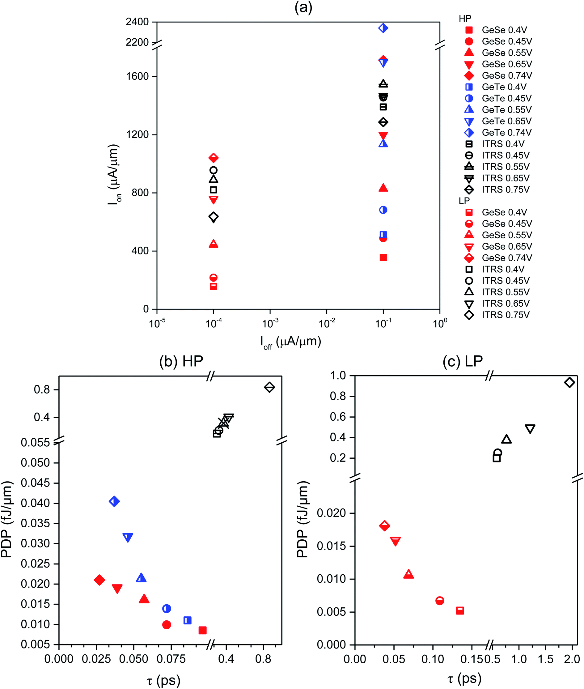 | ||
| Fig. 3 (a) Ion vs. Ioff and (b and c) delay time (τ) vs. power dissipation (PDP) of the ML GeSe and GeTe TFETs (Vdd = 0.4–0.74 V) against those of the ITRS requirements for HP and LP devices (2015 version). | ||
| Vdd (V) | SS (mV dec−1) | Ion (HP) (μA μm−1) | τ (HP) (ps) | PDP (HP) (fJ μm−1) | Ion (LP) (μA μm−1) | τ (LP) (ps) | PDP (LP) (fJ μm−1) | |
|---|---|---|---|---|---|---|---|---|
| GeSe | 0.74 | 39 | 1715 | 0.027 | 0.021 | 1272 | 0.034 | 0.020 |
| 0.65 | 38 | 1200 | 0.039 | 0.019 | 759 | 0.052 | 0.016 | |
| 0.55 | 37 | 829 | 0.057 | 0.016 | 444 | 0.069 | 0.011 | |
| 0.45 | 36 | 489 | 0.072 | 0.010 | 217 | 0.109 | 0.007 | |
| 0.4 | 37 | 355 | 0.096 | 0.009 | 156 | 0.135 | 0.005 | |
| GeTe | 0.74 | 70 | 2342 | 0.037 | 0.041 | — | — | — |
| 0.65 | 69 | 1699 | 0.046 | 0.032 | — | — | — | |
| 0.55 | 66 | 1135 | 0.055 | 0.021 | — | — | — | |
| 0.45 | 63 | 683 | 0.072 | 0.014 | — | — | — | |
| 0.4 | 58 | 512 | 0.086 | 0.011 | — | — | — |
The device dynamic performance metrics are defined by the delay time 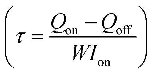 and power dissipation
 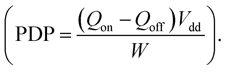 In the formula, Qon/off is the overall charge in the gate region for the on-/off-states, and W is the channel width. τ vs. PDP of the optimal ML GeSe and GeTe TFETs with Lg = 10 nm at Vdd = 0.4–0.74 V benchmarked with those of the ITRS requirements (2015 version) for the HP and LP devices, as shown in Fig. 3(b) and (c). We can see that the values of Ion and τ descend when the Vdd decreases from 0.74 to 0.4 V, while PDP values improve. A smaller τ indicates a faster switching speed, and a smaller PDP marks lower energy consumption. Thus, the left corner is favorable with respect to both fast switching speed and little energy consumption. For HP applications, the values of τ of ML GeSe and GeTe TFETs range from 0.027–0.096 ps and 0.037–0.086 ps, respectively, and the values of PDP of ML GeSe and GeTe TFETs range from 0.009–0.021 fJ μm−1 and 0.011–0.041 fJ μm−1, respectively. They are both smaller than one-tenth and one-twentieth of the ITRS HP requirements of 0.299–0.868 ps and 0.166–0.838 fJ μm−1, respectively. For LP applications, the values of τ and PDP of ML GeSe TFETs are 0.034–0.135 ps and 0.005–0.020 fJ μm−1, which are smaller than one-twentieth and one-fortieth of the ITRS LP requirements of 0.604–1.95 ps and 0.198–0.934 fJ μm−1, respectively.
The sub-threshold swing (SS) is defined as the linear relationship of Vg and lg![[thin space (1/6-em)]](https://www.rsc.org/images/entities/char_2009.gif) ID in the sub-threshold region, which is expressed as
ID in the sub-threshold region, which is expressed as  SS of the ML GeSe and GeTe TFETs are 36–39 and 58–70 mV dec−1 at Vdd = 0.4–0.74 V, respectively. SS of the ML GeSe TFETs is much smaller than that of the thermal diffusion limit of conventional FETs (of 60 mV dec−1).
The local device density of states (LDDOS) and transmission spectra of the optimal ML GeTe TFET for the HP application under on- and off-states at the Vdd of 0.74 and 0.4 V are shown in Fig. 4(a) and (b), respectively. The source-to-drain BTBT mechanism can be obviously seen from LDDOS. In the bias windows, the BTBT currents are generated because of the overlap of the source valence bands and drain conduction bands. When it is on-state and off-state, the BTBT barrier width is small and large, respectively. From the transport spectra in the right panels of Fig. 4, a narrower transport spectrum with a lower peak for the on-state is found at Vdd = 0.4 V, so that an obvious descend of the Ion is obtained.
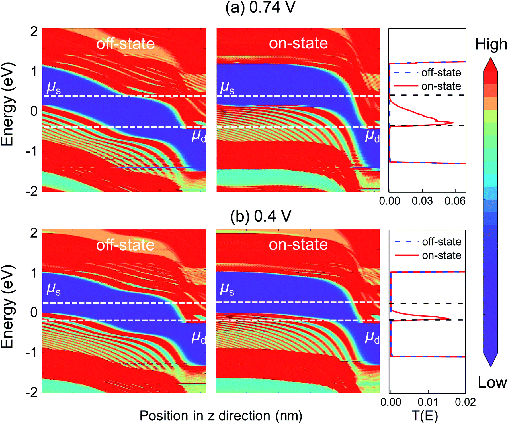 | ||
| Fig. 4 Local device density of states (LDDOS) and transport spectra of the ML GeTe TFET with a physical gate length of Lg = 10 nm for HP application with NS/ND = 0.1/5 × 1013 cm−2 at the Vdd of 0.74 V (a) and 0.4 V (b). | ||
NCTFET
A prototype negative capacitance TFET (NCTFET) is proposed to make Ion meet the standard of ITRS at a lower Vdd. We list the required thicknesses of four ferroelectric materials to make Ion exceed the ITRS demands at Vdd = 0.55 V in Table 3. Notably, for the ML GeTe TFET, Ion is 1135 μA μm−1, which dramatically raises to 1822 μA μm−1 by adding 50 nm-thick SrBi2Nb2O9 ferroelectric dielectric to construct the NCTFTE architecture for HP device, while 80 nm-thick SrBi2Nb2O9 is needed for the ML GeSe NCTFET to make the on-state current increase from 444 μA μm−1 to 892 μA μm−1 for LP devices. The required thicknesses of the HZO/PZT/BaTiO3 ferroelectric dielectrics are much larger, with 160/230/2300 nm for the ML GeSe NCTFETs and 90/120/1600 nm for the ML GeTe NCTFETs to reach the ITRS requirements. It is found that the NCTFET not only improves the corresponding Ion, but also has positive impacts on τ, which are shown in Table 3. The value of τ is decreased from 0.069 to 0.036–0.033 ps for the ML GeSe TFETs, while the τ decreased from 0.055 to 0.039–0.033 ps for the ML GeTe TFETs. For PDP, the values of the ML GeSe and GeTe NCTFETs are almost equal to those of the ML GeSe and GeTe TFETs. In all, we suggest SrBi2Nb2O9 among the checked ferroelectric dielectrics for both the ML GeSe and GeTe NCTFETs.| Ferroelectric dielectrics | α | β | γ | tFE (nm) | Ion (μA μm−1) | τ (ps) | PDP (fJ μm−1) | |
|---|---|---|---|---|---|---|---|---|
| GeSe | SrBi2Nb2O9 | −3.74 × 10⁸ | −9.4 × 10⁷ | 1.18 × 10⁹ | 80 | 892 | 0.036 | 0.010 |
| HZO | −1.99 × 10⁸ | 5.898 × 10⁹ | 0 | 160 | 908 | 0.033 | 0.010 | |
| PZT | −1.35 × 10⁸ | 3.05 × 10⁸ | −2.11 × 10⁷ | 230 | 920 | 0.033 | 0.010 | |
| BaTiO3 | −1 × 10⁷ | −8.9 × 10⁸ | 4.5 × 10¹⁰ | 3000 | 895 | 0.033 | 0.010 | |
| ITRS35 | LP | — | 890 | 0.766 | 0.375 | |||
| GeTe | SrBi2Nb2O9 | −3.74 × 10⁸ | −9.4 × 10⁷ | 1.18 × 10⁹ | 50 | 1822 | 0.033 | 0.021 |
| HZO | −1.99 × 10⁸ | 5.898 × 10⁹ | 0 | 90 | 1661 | 0.036 | 0.021 | |
| PZT | −1.35 × 10⁸ | 3.05 × 10⁸ | −2.11 × 10⁷ | 120 | 1569 | 0.038 | 0.021 | |
| BaTiO3 | −1 × 10⁷ | −8.9 × 10⁸ | 4.5 × 10¹⁰ | 1600 | 1559 | 0.039 | 0.021 | |
| ITRS35 | HP | — | 1546 | 0.370 | 0.315 |
Conclusions
In summary, we use the rigorous ab initio quantum transport simulation to explore the device performance limits of the 10 nm-gate-long ML GeSe and GeTe TFETs. At a supply voltage of 0.65–0.74 V, Ion of the ML GeSe and GeTe TFETs can meet the ITRS requirements for the LP and HP applications, respectively. Moreover, with the ferroelectric dielectric, we find that adding 80 and 50 nm-thickness of SrBi2Nb2O9 can elevate the Ion (LP) and Ion (HP) of the optimal ML GeSe and GeTe TFETs by 2 and 1.6 times to exceed the ITRS demands for the LP and HP devices, respectively, at a lower Vdd of 0.55 V. We expect our research to encourage future experimental investigations on the ML GeSe and GeTe NCTFETs at sub-10 nm nodes.Conflicts of interest
There are no conflicts to declare.Acknowledgements
This work was supported by the National Natural Science Foundation of China (No. 11704008, 91964101 and 11674005), the Basic Scientific Research Foundation of Beijing Municipal Education Commission (No. 110052971803/031), the Support Plan of Yuyou Youth and Yuyou Innovation Team from NCUT, and Science and Technology Innovation Activities for College Students from NCUT (No. 110051360019XN140/004).References
- D. B. Farmer, R. Golizadeh-Mojarad, V. Perebeinos, Y. M. Lin, G. S. Tulevski, J. C. Tsang and P. Avouris, Nano Lett., 2009, 9, 388–392 CrossRef CAS PubMed
.
- A. D. Franklin, M. Luisier, S.-J. Han, G. Tulevski, C. M. Breslin, L. Gignac, M. S. Lundstrom and W. Haensch, Nano Lett., 2012, 12, 758–762 CrossRef CAS PubMed
- D. Sarkar, X. Xie, W. Liu, W. Cao, J. Kang, Y. Gong, S. Kraemer, P. M. Ajayan and K. Banerjee, Nature, 2015, 526, 91–95 CrossRef CAS PubMed
- G. V. Resta, A. Leonhardt, Y. Balaji, S. De Gendt, P.-E. Gaillardon and G. De Micheli, IEEE Trans. Very Large Scale Integr. Syst., 2019, 27, 1486–1503 Search PubMed
- M. H. Lee, J. C. Lin, Y. T. Wei, C. W. Chen, W.-H. Hu, H.-K. Zhuang and M. Tang, Presented in part at the 2013 IEEE International Electron Devices Meeting (IEDM), Washington, DC, USA, 2013 Search PubMed
- C. Liu, P.-G. Chen, M.-J. Xie, S.-N. Liu, J.-W. Lee, S.-J. Huang, S. Liu, Y.-S. Chen, H.-Y. Lee, M.-H. Liao, P.-S. Chen and M.-H. Lee, Jpn. J. Appl. Phys., 2016, 55, 04EB08 CrossRef
- H. Zhao, Y. Mao, X. Mao, X. Shi, C. Xu, C. Wang, S. Zhang and D. Zhou, Adv. Funct. Mater., 2018, 28, 1704855 CrossRef
- M. Qiao, Y. Chen, Y. Wang and Y. Li, J. Mater. Chem. A, 2018, 6, 4119–4125 RSC
- E. S. Walker, S. R. Na, D. Jung, S. D. March, J. S. Kim, T. Trivedi, W. Li, L. Tao, M. L. Lee, K. M. Liechti, D. Akinwande and S. R. Bank, Nano Lett., 2016, 16, 6931–6938 CrossRef CAS PubMed
- P. Ares, F. Aguilar-Galindo, D. Rodriguez-San-Miguel, D. A. Aldave, S. Diaz-Tendero, M. Alcami, F. Martin, J. Gomez-Herrero and F. Zamora, Adv. Mater., 2016, 28, 6332–6336 CrossRef CAS PubMed
- S. Zhang, M. Xie, F. Li, Z. Yan, Y. Li, E. Kan, W. Liu, Z. Chen and H. Zeng, Angew. Chem., Int. Ed., 2016, 55, 1666–1669 CrossRef CAS PubMed
- D. Kecik, E. Durgun and S. Ciraci, Phys. Rev. B, 2016, 94, 205410 CrossRef
- Y. Guo, S. Zhou, Y. Bai and J. Zhao, ACS Appl. Mater. Interfaces, 2017, 9, 12013–12020 CrossRef CAS PubMed
- L. C. Gomes, A. Carvalho and A. H. Castro Neto, Phys. Rev. B, 2016, 94, 054103 CrossRef
- L. Xu, M. Yang, S. J. Wang and Y. P. Feng, Phys. Rev. B, 2017, 95, 235434 CrossRef
- F. Li, X. Liu, Y. Wang and Y. Li, J. Mater. Chem. C, 2016, 4, 2155–2159 RSC
- X. Lv, W. Wei, Q. Sun, F. Li, B. Huang and Y. Dai, Appl. Catal., B, 2017, 217, 275–284 CrossRef CAS
- K. Cheng, Y. Guo, N. Han, Y. Su, J. Zhang and J. Zhao, J. Mater. Chem. C, 2017, 5, 3788–3795 RSC
- Y. Huang, X. Chen, C. Wang, L. Peng, Q. Qian and S. Wang, Nanoscale, 2017, 9, 8616–8622 RSC
- L. Huang, F. Wu and J. Li, J. Chem. Phys., 2016, 144, 114708 CrossRef PubMed
- W. C. Yap, Z. Yang, M. Mehboudi, J.-A. Yan, S. Barraza-Lopez and W. Zhu, Nano Res., 2018, 11, 420–430 CrossRef CAS
- M. Brandbyge, J.-L. Mozos, P. Ordejón, J. Taylor and K. Stokbro, Phys. Rev. B: Condens. Matter Mater. Phys., 2002, 65, 165401 CrossRef
- J. M. Soler, E. Artacho, J. D. Gale, A. García, J. Junquera, P. Ordejón and D. Sánchez-Portal, J. Phys.: Condens. Matter, 2002, 14, 2745–2779 CrossRef CAS
- Atomistix ToolKit version 2017.2, QuantumWise A/S, Copenhagen, Denmark, http://www.quantumwise.com/ Search PubMed
- J. P. Perdew, K. Burke and M. Ernzerhof, Phys. Rev. Lett., 1996, 77, 3865–3868 CrossRef CAS PubMed
- D. J. Chadi, Phys. Rev. B: Solid State, 1977, 16, 1746–1747 CrossRef
- S. Datta and H. van Houten, Phys. Today, 1996, 49, 70 CrossRef
- G. A. Salvatore, D. Bouvet and A. M. Ionescu, Presented in part at the 2008 IEEE International Electron Devices Meeting, San Francisco, CA, USA, 2009 Search PubMed
- A. Starkov and I. A. Starkov, Ferroelectrics, 2014, 461, 50–60 CrossRef CAS
- S. Salahuddin and S. Datta, Nano Lett., 2008, 8, 405–410 CrossRef CAS PubMed
- A. Saeidi, F. Jazaeri, I. Stolichnov and A. M. Ionescu, IEEE Trans. Electron Devices, 2016, 63, 4678–4684 Search PubMed
- C. Jiang, M. Si, L. Renrong, J. Xu, P. D. Ye and M. A. Alam, IEEE J. Electron Devices Soc., 2018, 6, 189–194 CAS
- F. Liu, Y. Zhou, Y. Wang, X. Liu, J. Wang and H. Guo, npj Quantum Mater., 2016, 1, 16004 CrossRef
- H. Li, P. Xu and J. Lu, Nanoscale, 2019, 11, 23392–23401 RSC
- International Technology Roadmap for Semiconductors (ITRS), Semiconductor Industry Association, http://www.itrs2.net/ Search PubMed.
Footnote |
| † Electronic supplementary information (ESI) available: Transfer characteristics of the ML GeSe and GeTe TFETs (Lg = 10 nm) with NS/ND at the Vdd of 0.74 V. See DOI: 10.1039/d0ra02265a |
| This journal is © The Royal Society of Chemistry 2020 |