DOI:
10.1039/D0RA02122A
(Paper)
RSC Adv., 2020,
10, 21206-21221
Efficient and chromaticity stable green and white organic light-emitting devices with organic–inorganic hybrid materials†
Received
6th March 2020
, Accepted 21st May 2020
First published on 3rd June 2020
Abstract
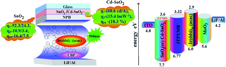
Efficient inverted bottom emissive organic light emitting diodes (IBOLEDs) with tin dioxide and/or Cd-doped SnO2 nanoparticles as an electron injection layer at the indium tin oxide cathode:electron transport layer interface have been fabricated. The SnO2 NPs promote electron injection efficiently because their conduction band (−3.6 eV) lies between the work function (Wf) of ITO (4.8 eV) and the LUMO of the electron-transporting molecule (−3.32 eV), leading to enhanced efficiency at low voltage. The 2.0% SnO2 NPs (25 nm) with Ir(ddsi)2(acac) emissive material (SnO2 NPs/ITO) have an enhanced current efficiency (ηc, cd A−1) of 52.3/24.3, power efficiency (ηp, lm W−1) of 10.9/3.4, external quantum efficiency (ηex, %) of 16.4/7.5 and luminance (L, cd m−2) of 28![[thin space (1/6-em)]](https://www.rsc.org/images/entities/char_2009.gif) 182/1982. A device with a 2.0% Cd-doped SnO2 layer shows higher ηc (60.6 cd A−1), ηp (15.4 lm W−1), ηex (18.3%) and L (26858 cd m−2) than SnO2 devices or control devices. White light emission was harvested from a mixture of Cd–SnO2 NPs and homoleptic blue phosphor Ir(tsi)3; the combination of blue emission (λEL = 428 nm) from Ir(tsi)3 and defect emission from Cd–SnO2 NPs (λEL = 568 nm) gives an intense white light with CIE of (0.31, 0.30) and CCT of 6961 K. The white light emission [CIE of (0.34, 0.35) and CCT of 5188 K] from colloid hybrid electrolyte BMIMBF4–SnO2 is also discussed.
182/1982. A device with a 2.0% Cd-doped SnO2 layer shows higher ηc (60.6 cd A−1), ηp (15.4 lm W−1), ηex (18.3%) and L (26858 cd m−2) than SnO2 devices or control devices. White light emission was harvested from a mixture of Cd–SnO2 NPs and homoleptic blue phosphor Ir(tsi)3; the combination of blue emission (λEL = 428 nm) from Ir(tsi)3 and defect emission from Cd–SnO2 NPs (λEL = 568 nm) gives an intense white light with CIE of (0.31, 0.30) and CCT of 6961 K. The white light emission [CIE of (0.34, 0.35) and CCT of 5188 K] from colloid hybrid electrolyte BMIMBF4–SnO2 is also discussed.
1. Introduction
Organic light-emitting diodes (OLEDs) have been attractive for use in displays and solid-state lighting due to their flexibility, color contrast, color purity, low power-consumption, etc.1–3 Inverted bottom emissive OLEDs (IBOLEDs) with a bottom cathode are more advantageous than conventional OLEDs due to their minimized voltage drop. However, efficient electron injection is a current issue in IBOLEDs due to the lack of suitable cathode materials. Because of its high optical transparency and electrical conductivity, ITO is used as a cathode in IBOLEDs, but its high work function (4.8 eV) limits electron injection from ITO to an electron transporting layer (ETL). Electron injection has been enhanced by incorporation of a metallic layer with a low work function4 and doped ETL with lithium,5 cesium6–8 or rubidium.9 However, these methods lead to operational instability by oxidation of the metal or diffusion of the metal dopant10,11 and they need a high-cost vacuum process. These issues can be overcome by solution processable methods using conjugated polymers12 and n-type metal oxides,13–15 zinc oxide,16,17 titanium dioxide18 and zirconium dioxide19 as an electron injection layer (EIL). However, these methods require a high annealing temperature (300 °C) for better electron transportation. ZnO nanoparticles (NPs) have been used as an efficient EIL20–25 with a low process temperature (˂100 °C), but ZnO is unstable under UV illumination.26 Therefore, it was decided to use SnO2 and Cd-doped SnO2NPs with a wide band gap and low sensitivity towards UV light.27,28
White light emission is a hot topic of research because white light emitting devices (WOLEDs) would drastically reduce global electricity consumption. Organic dyes, lanthanide-doped semiconducting NPs, quantum dots,29–31 DNA,32 nano dye polymer conjugates,33 core–shell materials34 and ZnO NPs with graphene and GaN35 are used for white light emission. Near-UV chips with a blend of red, green and blue phosphors or a combination of yellow and blue emitters have been used for white light generation because of the high CCT (correlated color temperature) of these LEDs.36,37 Though blue light emission from SnO2NPs has been widely studied,38–40 doping of SnO2 by metal ions with various ionic radii, different structures, electronegativities and valency differences leads to additional defect emission.41 Cadmium has been used as a dopant due to its lower valency and larger ionic radius than Sn4+ ions and it generates various defects responsible for visible emission. Herein, we report efficient IBOLEDs using SnO2 and Cd–SnO2NPs as EILs with a green phosphorescent emissive layer. The fabricated device (2% SnO2NPs/ITO) exhibits a maximum current efficiency (ηc, cd A−1) of 52.3/24.3, power efficiency (ηp, lm W−1) of 10.9/3.4, external quantum efficiency (ηex, %) of 16.4/7.5 and luminance (L, cd m−2) of 28182/1982. Also, a device with a 2.0% Cd-doped SnO2 layer shows a higher ηc (60.6 cd A−1), ηp (15.4 lm W−1), ηex (18.3%) and L (26858 cd m−2) than SnO2 devices or control devices. The white emission was harvested from a mixture of Cd–SnO2 NPs and homoleptic blue phosphor Ir(tsi)3; the combination of blue emission (λEL = 428 nm) from Ir(tsi)3 and defect emission from Cd–SnO2 NPs (λEL = 568 nm) gives an intense white light (CIE (0.31, 0.30); CCT = 6961 K).
2. Experimental
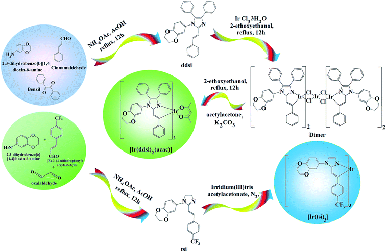
2.1. (E)-1-(2,3-Dihydrobenzo[b][1,4]dioxin-6-yl)-4,5-diphenyl-2-styryl-1H-imidazole (ddsi)
A mixture of benzil (5 mmol), (E)-3-(4-fluorophenyl)acrylaldehyde (5 mmol), 1,4-benzodioxane-6-amine (6 mmol) and ammonium acetate (61 mmol) was refluxed (ethanol; 12 h; N2 stream). The reaction mixture was chilled and the yellow solid of ddsi was separated42 (ethanol; 12 h; N2 stream). 1H NMR (400 MHz, CDCl3): δ (ppm): 4.36 (s, 4H), 6.7 (m, 3H), 6.99 (s, 2H), 7.14–7.22 (m, 5H), 7.30–7.32 (m, 6H), 7.48 (d, 4H). 13C NMR (100 MHz, CDCl3): δ (ppm): 64.3, 112.8, 114.5, 114.6, 121.9, 123, 125.4, 126.4, 127.5, 128.8, 129.3, 131.9, 133.1, 133.4, 135.2, 137, 137.0, 147.6. MS: m/z. 458.55 [M+]. Calcd 458.35. FT-IR (cm−1): 690, 762, 846, 935, 1006, 1018, 1230, 1515, 1606, 1620, 1650, 2850, 2960, 3070, 3420.
2.2. Iridium(III)-bis-(E)-1-(2,3-dihydrobenzo[b][1,4]dioxin-6-yl)-4,5-diphenyl-2-styryl-1H-imidazole acetylacetonate [Ir(ddsi)2(acac)]
A mixture of ddsi (2.2 mmol) and iridium(III) chloride trihydrate (1 mmol) in 2-ethoxyethanol:H2O (3:1) was refluxed (N2; 120 °C) and the formed dimer (1 mmol) was refluxed (120 °C; N2) with K2CO3 (2.5 mmol) and acetyl acetone (2.2 mmol) in 2-ethoxyethanol (5 ml).46 The green-colored acetylacetonate iridium complex was characterized by spectral techniques (Scheme 1). 1H NMR (400 MHz, CDCl3): δ (ppm): 1.21 (d, 2H), 1.47–1.72 (m, 2H), 3.39 (m, 2H), 4.36 (s, 4H), 4.44 (d, 2H), 5.88 (m, 2H), 5.98 (m, 2H), 6.2 (d, 2H), 6.49 (m, 2H), 7.11–7.14 (m, 6H), 7.21–7.26 (m, 12H), 7.42 (m, 8H). 13C NMR (100 MHz, CDCl3): δ (ppm): 26.18, 44.02, 46.82, 64.31, 105.49, 105.72, 113.26, 115.82, 121.86, 126.45, 127.02, 128.09, 128.79, 132.01, 134.31, 134.94, 147.54. MS: m/z. 1207.40 [M+]. Calcd 1207.31.
 |
| | Scheme 1 Synthetic route for emissive materials. | |
2.3. (E)-1-(2,3-Dihydrobenzo[b][1,4]dioxin-5-yl)-2-(4-(trifluoromethyl)styryl)-1H-imidazole (tsi)
A mixture of (E)-3-(4-trifluoromethylphenyl)acrylaldehyde (1 mmol), glyoxal (1 mmol), 2,3-dihydro-1,4-benzodioxane-6-amine (1 mmol) and ammonium acetate (1 mmol) in ethanol was refluxed (12 h; N2). The mixture was cooled, filtered and column chromatographed (9:1 benzene:ethyl acetate). Yield: 71%. 1H NMR (400 MHz, CDCl3): δ (ppm): 4.39 (s, 4H), 6.7 (m, 3H), 6.99 (s, 2H), 7.23–7.3 (m, 3H), 7.40–7.5 (m, 3H). 13C NMR (100 MHz, CDCl3): δ (ppm): 64.3, 112.8, 114.5, 115.63, 115.77, 121.96, 124.28, 125.19, 125.48, 126.79, 130.26, 133.45, 137.00, 137.61, 138.51, 147.68. MS: m/z. 372.34 [M+] calcd 372.21. FT-IR (cm−1): 698, 832, 886, 945, 1027, 1156, 1228, 1505, 1600, 1632, 1644, 2860, 3426.
2.4. fac-Tris[2-(4-trifluoromethylstyryl)-1-(2,3-dihydrobenzo[b][1,4]dioxin-8-yl)-1H-imidazolynato-C2,N1]iridium(III) [Ir(tsi)3]
A mixture of tsi (7.83 mmol), iridium(III) trisacetylacetonate (1.56 mmol) and glycerol (9 ml) was refluxed under an N2 stream for four days. After cooling, the reaction mixture was extracted with dichloromethane and the separated fac-isomer Ir(dsi)3 was purified by hexane washing (Scheme 1). 1H NMR (400 MHz, CDCl3): δ (ppm): 4.36 (s, 6H), 4.44 (d, 3H), 5.06 (t, 3H), 5.21 (t, 3H), 5.88–5.98 (m, 6H), 6.19–6.2 (m, 3H), 6.49–6.53 (m, 4H), 7.23 (m, 6H), 7.40 (m, 6H). 13C NMR (100 MHz, CDCl3): δ (ppm): 56.05, 59.02, 64.33, 103.48, 105.72, 111.76, 114.38, 121.39, 123.36, 124.2, 125.1, 126.7, 127.00, 128.9, 129.5, 130.2, 132.00, 138.22, 147.56. MS: m/z. 1310.30 [M+]; calcd 1310.19.
2.5. 1-Butyl-3-methylimidazolium tetrafluoroborate [BMIMBF4]
About 10.8 g of n-bromobutane and 8.2 g of 1-methyimidizole were refluxed under stirring (70 °C; 48 h). The reaction mixture was washed with ethyl acetate to eliminate the unreacted reagents and the solvent was evaporated to get the pale yellow liquid of 1-butyl-3-methylimidazolium bromide (BMIMBr).42 About 6.57 g of BMIMBr and 3.29 g of NaBF4 were refluxed in acetone under stirring at low temperature (10 h). The reaction mixture was extracted with dichloromethane and dried (80 °C; 2 h).42 1H NMR (300 MHz, CDCl3): δ (ppm): 0.9 (s, 1H), 0.96 (m, 3H), 1.33 (m, 2H), 1.77 (m, 2H), 3.73 (m, 2H). 13C NMR (76 MHz, CDCl3): δ (ppm): 13.89, 20.60, 33.22, 44.45, 54.06, 122.85, 123.00, 137.07.
2.6. Nanocrystalline SnO2and Cd-doped SnO2
To a reaction mixture of tin tetrachloride pentahydrate (SnCl4·5H2O) without or with cadmium chloride, moderate PEG in distilled water and aq. NH3 were added drop by drop under stirring (pH 9). The milky colloidal solution was subjected to stirring for 3 h followed by centrifugation and the formed SnO2 and/or Cd-doped SnO2 was washed with distilled water, dried (80 °C; 12 h) and calcinated (400 °C; 2 h; heating rate 10 °C min−1) to form SnO2 and or pale yellow colored Cd-doped SnO2 solid.
2.7. BMIMBF4–Cd–SnO2 colloidal hybrid electrolyte
About, 0.1 mmol of cationic IL BMIMBF4 was added to Cd–SnO2 in CHCl3 dispersion and sonicated for 2 h. The formed light yellow viscous BMIMBF4–Cd–SnO2 colloidal hybrid electrolyte was used to generate white emission.
2.8. Characterization
The powder X-ray diffractogram (XRD) was recorded with a PANalytical X'Pert PRO diffractometer using Cu Kα rays at 1.5406 Å with a tube current of 30 mA at 40 kV. The energy dispersive X-ray spectra (EDS) were recorded with a JEOL JSM-5610 scanning electron microscope (SEM) equipped with a back electron (BE) detector. The sample was placed on an adhesive carbon slice supported on copper stubs and coated with 10 nm thick gold using a JEOL JFC-1600 auto fine coater prior to measurement. TEM analysis was carried out using a JEOL JEM 2100 high-resolution transmission electron microscope (HR-TEM) with 200 kV voltage. The fluorescence lifetime was measured in nanoseconds with a time correlated single photon counting (TCSPC) spectrometer and Horiba Fluorocube-01-NL lifetime system with a nano LED (pulsed diode excitation source) as the excitation source and TBX-PS as the detector. The UV-vis absorption and fluorescence spectra were recorded with a PerkinElmer Lambda 35 spectrophotometer and a PerkinElmer LS55 spectrofluorometer, respectively. The absolute quantum yield (PLQY) of the emissive material was determined in dichloromethane with a 0.5 M H2SO4 solution of quinine (0.54) as reference using a fluorescence spectrometer Model-F7100 and using the equation:  , where ϕunk and ϕstd are the radiative quantum yield of the sample and standard; Iunk and Istd are the integrated emission intensities of sample and standard, respectively; Aunk and Astd are the absorbance of sample and standard, respectively; and ηunk and ηstd are the refractive index of sample and standard solution, respectively. The solid-state quantum yield was measured on a quartz plate with an integrating sphere.
2.9. Fabrication of OLED
Green OLEDs with a configuration of ITO/x wt% SnO2 (x = 0.5, 1.0, 1.5 or 2.0%) or x wt% Cd–SnO2 (2.0%)/3TPYMB (40 nm)/CBP:Ir(ddsi)2(acac)/MoO3(10 nm)/Au(100 nm) were fabricated, where ITO and Au are used as the cathode and anode conductors, respectively. Tris[3-(3-pyridyl)mesityl]borane (3TPYMB), Ir(ddsi)2(acac) and MoO3 are used as the electron transport layer, emissive layer and barrier-reducing hole injection/electron-blocking layer, respectively. Ir(ddsi)2(acac) doped 4,4-N,N-dicarbazolbiphenyl (CBP) with a doping ratio of 8 wt% (40 nm) was used as a green-emitting layer. All layers were deposited on an ITO plate by a thermal evaporation unit with a glove box under optimized evaporation rates. The thickness was monitored using a quartz crystal digital thickness monitor. The current density–voltage and light intensity of the OLEDs were measured using a Keithley 2400 source measuring unit. The EL spectra of the devices were carried out in an ambient atmosphere without further encapsulation.
2.10. Computational details
The optimized geometry, highest occupied molecular orbital (HOMO) and lowest unoccupied molecular orbital (LUMO) contour map of Ir(ddsi)2(acac) and Ir(tsi)3 were studied with the Guassian-09 package [DFT/B3LYP/6-31G (d, p)].43
3. Results and discussion
3.1. Morphological properties
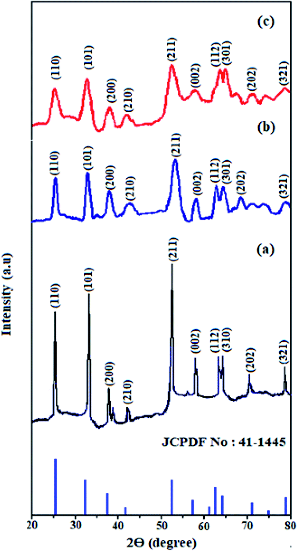
Fig. 1 shows the XRD patterns of pristine SnO2, Cd-doped SnO2 and HMIMBF4–Cd–SnO2 nanoparticles. All diffraction peaks are assigned to the tetragonal rutile phases of tin oxide (JCPDS no. 41-1445, a = 4.740 Å, c = 3.190 Å). The high-intensity peaks around 26.0°, 33.0° and 53.0° correspond to the (1 1 0), (1 0 1), and (2 1 1) planes of tetragonal SnO2, respectively. The absence of any other unassigned peak indicates the purity of the synthesized crystalline SnO2, Cd-doped SnO2 and BMIMBF4–Cd–SnO2 NPs. The broadened peaks of Cd-doped SnO2 and BMIMBF4–Cd–SnO2 imply that the cadmium dopant increases the concentration of lattice imperfections due to a decrease in internal micro strain within the matrix and confirmed the presence of small crystallites.44 Using Scherrer's formula, the average crystallite size and surface area of pristine SnO2, Cd-doped SnO2 and BMIMBF4–Cd–SnO2 hybrid electrolyte nanocrystals were found to be 4.8, 2.5 and 18.25 nm and 220.5, 423.3 and 57.98 m2 g−1, respectively.44
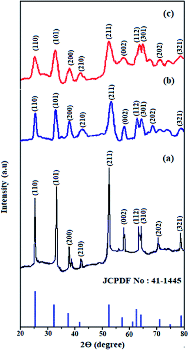 |
| | Fig. 1 XRD pattern of SnO2 (a), Cd-doped SnO2 (b) and HMIMBF4–Cd–SnO2 (c). | |
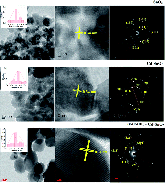
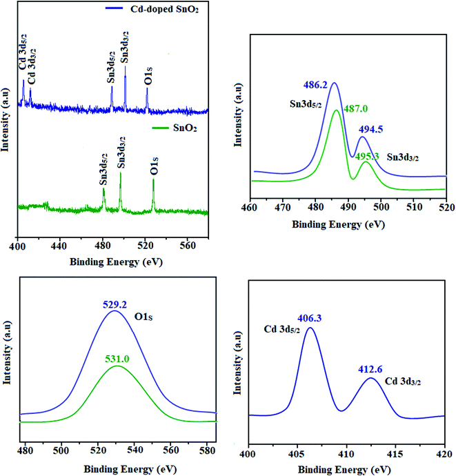
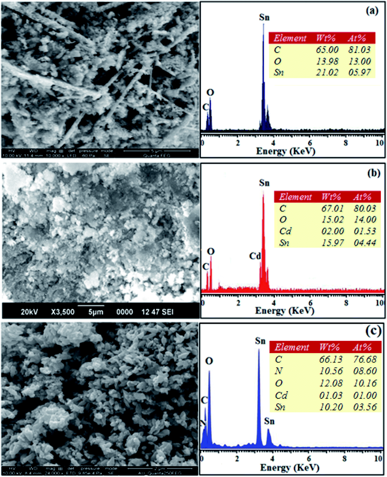
The SEM images of pristine SnO2, Cd-doped SnO2 and BMIMBF4–Cd–SnO2 nanomaterials reveal agglomeration of nanoparticles (Fig. 2). The energy dispersive X-ray spectra confirm the presence of constituent elements. The observed carbon peaks are due to the carbon stub on which the samples were dispersed and the absence of other elements reveals the purity of the nanomaterial. The EDX spectra of cationic BMIMBF4–Cd–SnO2 show the presence of carbon, nitrogen, cadmium and tin, which confirms the binding of BMIMBF4 with Cd–SnO2. The HR-TEM images of pristine SnO2, Cd-doped SnO2 and BMIMBF4–Cd–SnO2 hybrid electrolyte confirm the nanoparticulate character. The measured average particle sizes from the TEM image are larger than those deduced from the XRD results because the nanoparticles associate among themselves (Fig. 3). TEM images at higher magnification display the lattice fringes and the observed interplanar distance is 0.34 nm corresponding to the (1 1 0) plane of rutile SnO2 (Fig. 3). The SAED of pristine SnO2, Cd-doped SnO2 and BMIMBF4–Cd–SnO2 hybrid electrolyte shows bright concentric circles belonging to the planes (1 1 0), (1 0 1), (2 1 1) and (1 1 2), confirming the polycrystalline tetragonal structure (Fig. 3). X-ray photoelectron spectroscopy (XPS) was used to characterize the composition of pristine SnO2 and Cd-doped SnO2 nano-material and the spectrum shows the presence of the constituent elements (Fig. 4). The carbon peak is attributed to the residual carbon from the sample and adventitious hydrocarbon from the XPS instruments and it is not indicated. Compared to pristine SnO2, the binding energies of Sn 3d5/2 and 3d3/2 in Cd-doped SnO2NPs decreased from 487.0 to 486.2 eV and from 495.3 to 494.5 eV, respectively, which may be ascribed to there being insufficient oxygen.45 The symmetric Sn 3d peaks and XRD results confirm the presence of Sn4+ ions. A slight shift in the binding energy of the O 1s transition peak from 531.0 to 529.2 eV was observed for Cd–SnO2. The binding energies of the Cd 3d5/2 and Cd 3d3/2 peaks at 406.3 eV and 412.6 eV, respectively, confirm the presence of Cd2+ in Cd–SnO2 nanoparticles.46
 |
| | Fig. 2 SEM image with EDX of pristine SnO2 (a), Cd-doped SnO2 (b) and BMIMBF4–Cd SnO2 (c). | |
 |
| | Fig. 3 TEM images and SAED of SnO2 (a), Cd–doped SnO2 (b) and BMIMBF4–Cd–SnO2 (c). | |
 |
| | Fig. 4 X-ray photoelectron spectra of pristine SnO2 and Cd-doped SnO2. | |
3.2. Optical properties
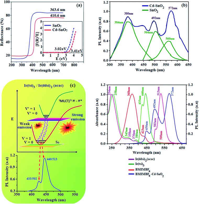
The absorption at 363.6 nm (pristine SnO2) and 410.6 nm (Cd-doped SnO2) may be attributed to the band gap transition and indicates the existence of highly crystalline SnO2. The band gaps of pristine SnO2 and Cd-doped SnO2 can be estimated from a plot of (αhν)2 versus photon energy as 3.41 and 3.02 eV, respectively.47 This reduction in band gap compared with bulk SnO2 (3.62 eV) may be attributed to the formation of impurity bands created by oxygen vacancies/defects.48,49 The absorption of BMIMBF4–Cd–SnO2 at 351 nm is due to the π–π* transition of the imidazolium ring and a weak tail above 400 nm is attributed to the presence of different associated structures of the imidazolium ring formed due to electrostatic interaction among the π-orbitals.49 The observed tail peak can be attributed to scattering phenomena induced by inorganic nanoparticles. The absorption spectrum of BMIMBF4–Cd–SnO2 dispersion is dominated by the strong absorption of Cd–SnO2NPs that overwhelms the contribution from BMIMBF4. The improvement in optical absorption of BMIMBF4–Cd–SnO2 in the visible region is associated with the synergistic effect of the two main components of Cd–SnO2 and BMIMBF4 (Fig. 5).
 |
| | Fig. 5 (a) Diffuse reflectance spectra; (b) emission spectra of pristine SnO2 and Cd-doped SnO2; (c) Frank–Condon electronic transition of Ir(tsi)3 and Ir(ddsi)2(acac); and (d) UV and PL spectra of Ir(tsi)3, Ir(ddsi)2(acac), BMIMBF4 and BMIMBF4–Cd–SnO2. | |
The emission spectra of Cd-doped SnO2 NPs and pristine SnO2 (380, 492 and 572 nm) are shown in Fig. 5. The spectra are broad and asymmetric with a peak centered at 504 nm. Deconvolution of this broad PL peak reveals three peaks at 384, 504 and 560 nm. The band at 384 nm is ascribed to band gap emission and the peaks at ∼504 (2.46 eV) and 560 nm (2.2 eV) are composed of green and yellow emissions, respectively. The green and yellow emissions are attributed to the recombination of excited electrons trapped in the donor level created by bulk oxygen vacancies with holes in the acceptor level formed by surface oxygen vacancies coordinated with tin atoms at different angles.50,51 The yellow emission originates from the recombination of trapped electrons in the singly ionized surface bridging oxygen vacancies with holes in the valence band52 (Scheme 1). The green emission at 504 nm of SnO2 NPs is blue-shifted to 492 nm for Cd-doped SnO2 and the yellow emission at 560 nm is red-shifted to 572 nm. Doping with cadmium enhances the yellow emission and suppresses the green emission due to an increase in the concentration of bulk oxygen vacancies at the donor level because of oxygen non-stoichiometry created by the replacement of Sn4+ ions by Cd2+ ions. As the ionic radius of the dopant Cd2+ (99 pm) is larger than that of Sn4+ (83 pm), substitution of Sn4+ ions by Cd2+ ions is unlikely. Hence, the other possibility is the existence of Cd2+ ion in the inter-lattice position. The variation in the oxidation states of tin and cadmium suggests the creation of oxygen defects. The interstitial based cadmium ions and the oxygen defects create impurity energy levels which are responsible for the observed emission. The intensity of Cd-doped SnO2 is enhanced over pristine SnO2 due to the high concentration of surface oxygen vacancies as well as singly ionized oxygen vacancies because of its smaller size. The pure BMIMBF4 ionic liquid exhibits an emission band centered around 368 nm with a shoulder on 423 nm and the band profile extends beyond 500 nm when excited at 340 nm. The decay of bare BMIMBF4 and BMIMBF4–Cd–SnO2 shows a triexponential function: the major component has a lifetime varying between 462 and 578 ps (90%) with two other minor components of 3.0 ns (7%) and 8.3 ns (3%) (Fig. 6). The average lifetime depends upon the permanent time of the carriers with the number of de-excitation pathways. The energy transfer between BMIMBF4 and Cd–SnO2 may be responsible for increasing the lifetime of BMIMBF4–Cd–SnO2. As the only photoluminescent component of BMIMBF4–Cd–SnO2 is the imidazolium moiety, the modification in PL decay was induced in BMIMBF4, which reveals charge transfer between BMIMBF4 and Cd–SnO2 (Table 1).40
 |
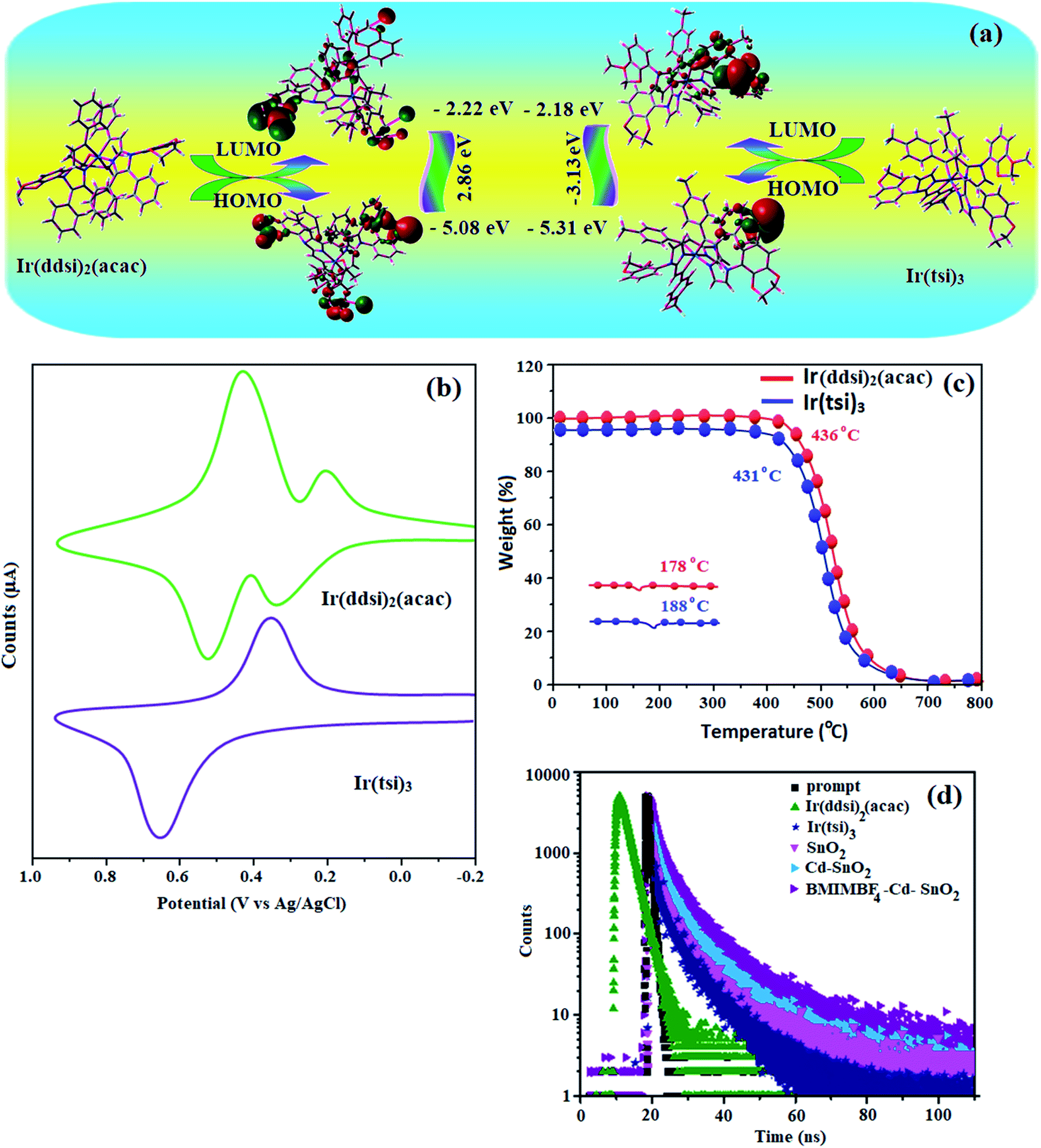
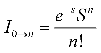
| | Fig. 6 (a) Fortier molecular orbital contour map of Ir(ddsi)2(acac) and Ir(tsi)3. (b) Cyclic voltammogram. (c) DSC and TGA curve of Ir(ddsi)2(acac) and Ir(tsi)3. (d) Lifetime decay curve. | |
Table 1 Optical and thermal properties of Ir(tsi)3 and Ir(ddsi)2(acac)
| Parameters |
Ir(tsi)3 |
Ir(ddsi)2(acac) |
| λab (nm) |
258, 343, 380 |
254, 358, 376 |
| λem (nm) |
433, 440 |
502, 513 |
| Td (°C) |
431/188 |
436/178 |
| ϕ |
0.98 |
0.82 |
| HOMO/LUMO (eV) |
−5.31/−2.18 |
−5.08/−2.22 |
| Eg (eV) |
−3.13 |
2.86 |
| τ (ns) |
1.8 |
2.3 |
| kr × 108 (s−1) |
5.4 |
3.6 |
| knr × 108 (s−1) |
0.02 |
0.07 |
3.3. Characterization of emissive materials
Fig. 5 shows the UV-vis absorption (λabs) spectra of the organometallic complexes, Ir(ddsi)2(acac) and Ir(tsi)3 in CH2Cl2. The intense absorptions in the ultraviolet region at 254 nm for Ir(ddsi)2(acac) and 258 nm for Ir(tsi)3 are assigned to a spin-allowed ligand-centered transitions. The other two bands of Ir(ddsi)2(acac) (358 and 376 nm) and Ir(tsi)3 (343 and 380 nm) confirmed the spin-allowed MLCT transitions: ground state to singlet excited state [1MLCT ← S0] and triplet excited state [3MLCT ← S0]. Both transitions originate from the interaction of the ligand with the iridium center of Ir(ddsi)2. The intensity of the 3MLCT ← S0 transition is closest to the 1MLCT ← S0 transition, which shows that the 3MLCT ← S0 transition is strongly symmetry allowed by spin–orbit coupling.53–60 The spin–orbit coupling was enhanced by the closeness of π–π* and MLCT and the heavy-atom effect of the iridium(III) complexes. The two phosphors Ir(ddsi)2(acac) and Ir(tsi)3 show strong luminescence in solution and solid. The broad emissive spectra of Ir(ddsi)2(acac) show green emission at 513 and 502 nm and Ir(tsi)3 shows blue emission at 433 and 440 nm (Fig. 5). The broad spectra reveal that the excited triplet states of Ir(ddsi)2(acac) and Ir(tsi)3 possess a predominantly 3MLCT character. Generally, the phosphorescence spectra from ligand-centered 3π–π* and 3MLCT states have a vibronic and broad shape.47–50 The absence of vibronic structured emission from organometallic complexes confirmed the MLCT nature of the emission and it was further confirmed by the phosphorescence lifetimes of 2.3 and 1.8 μs, respectively (Fig. 6). The wave function (Φ) of the triplet state (ΦT) is a mixture of ΦT (π–π*) and ΦT (MLCT);61 ΦT = aΦT (π–π*) + bΦT (MLCT) [a and b are normalized coefficients, ΦT (π–π*) and ΦT (MLCT) are the wave functions of 3(π–π*) and 3(MLCT) excited states, respectively: when a > b, the triplet state is dominated by 3π–π*; when b > a, the triplet state is dominated by the 3MLCT excited state]. The observed two peaks of Ir(ddsi)2(acac) (513 and 502 nm) and Ir(tsi)3 (433 and 440 nm) may attributed to the Franck–Condon electronic transition from the vibrational level of the triplet state (3MLCT/3π–π*) to the ground state (S0) (Fig. 5). The peak with dominant intensity stemmed from the ν′ = 0 to ν = 0 transition of 3MLCT/3π–π* to S0 whereas a shoulder peak with lower intensity derived from the ν′ = 0 to ν = 1 electronic transition.62–64 The gain in intensity is expressed as  , where S is the Huang–Rhys factor, correlated to the intensities of vibration from the excited 3MLCT/3π–π* state to the ground state (S0),
  ; ω is the vibrational frequency, M is the reduced mass, and ΔQ is the displacement of potential energy surfaces between the S0 and excited states. The structural distortion upon excitation is explained by the ratio of the height of the two emission peaks
  .
.
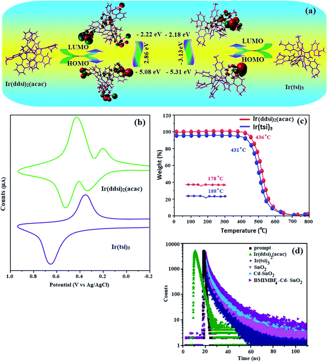
From the radiative lifetime and PL quantum yield of Ir(ddsi)2(acac) (τ = 2.3 μs; Φ = 0.82) and Ir(tsi)3 (τ = 1.8 μs; Φ = 0.98), radiative (kr) and non-radiative (knr) decay rate constants have been calculated from Φ = ΦISC {kr/(kr + knr)}, kr = Φ/τ, knr = (1/τ) − (Φ/τ) and τ = (kr + knr)−1 (Φ is quantum yield; τ is lifetime; and ΦISC is intersystem-crossing yield).65–69 The rate constants reveal that radiative emission [3.6 × 10⁸ s−1 for Ir(ddsi)2(acac); 5.4 × 10⁸ s−1 for Ir(tsi)3] is predominant over non-radiative transition [0.07 × 10⁸ s−1 for Ir(ddsi)2(acac); 0.02 × 10⁸ s−1 for Ir(tsi)3]. From DFT [B3LYP/6-31G(d,p)] analysis, it was shown that the HOMO in homoleptic Ir(tsi)3 is predominantly distributed over N-side coupling whereas the LUMO is localized on one of the C^N ligands of the iridium complex (Fig. 6). The heteroleptic Ir(ddsi)2(acac) complex exhibits a distorted octahedral geometry around the iridium atom with two cyclo-metalated ddsi ligands and one ancillary acetylacetonate (acac) ligand. The ddsi ligand adopts an eclipsed configuration and two nitrogen atoms N(5) and N(7) reside at the trans-N,N chelate disposition and the Ir–N distance lies between 2.08 and 2.10 Å. The cyclo-metalated carbon atoms C(12) and C(21) are mutually cis around the iridium atom and the Ir–C distance lies between 2.04 and 2.08 Å. Due to the stronger Ir–C interaction of the ddsi ligand, Ir–C bonds orient at the trans disposition. Electron-rich phenyl fragments of Ir(ddsi)2(acac) show a trans effect; thus the trans-C,C geometry is thermodynamically of higher energy and is kinetically more labile (transphobic) which is confirmed by the shorter Ir–C bond length (Ir–Cav = 2.04 Å) relative to the Ir–N bond length (Ir–Nav = 2.06 Å).57,59 The electrochemical stability of the complexes was confirmed by a reversible one-electron oxidation wave (Fig. 6). The HOMO energy [5.08 eV for Ir(ddsi)2(acac) and 5.31 eV for Ir(tsi)3] is determined from the oxidation potential and the ferrocenium/ferrocene redox couple energy [EHOMO (eV) = −(Eox + 4.8)] whereas the LUMO energy [2.22 eV for Ir(ddsi)2(acac) and 2.18 eV for Ir(tsi)3] is calculated by subtracting the optical band gap energy from EHOMO [ELUMO = EHOMO − 1239/λonset].70 To determine their suitability for device fabrication, thermal characterization was undertaken by TGA analysis (Fig. 6). The high values of Td/Tg [436/178 °C for Ir(ddsi)2(acac); 431/188 °C for Ir(tsi)3] reveal that the emissive materials Ir(ddsi)2(acac) and Ir(tsi)3 exhibit excellent thermal properties and could be subjected to vacuum-evaporation without decomposition.71–73 They could form morphologically stable amorphous films on thermal evaporation, which would reduce the phase separation on heating and improve the lifetime of the devices.
3.4. Electroluminescent studies
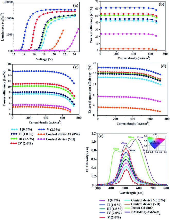
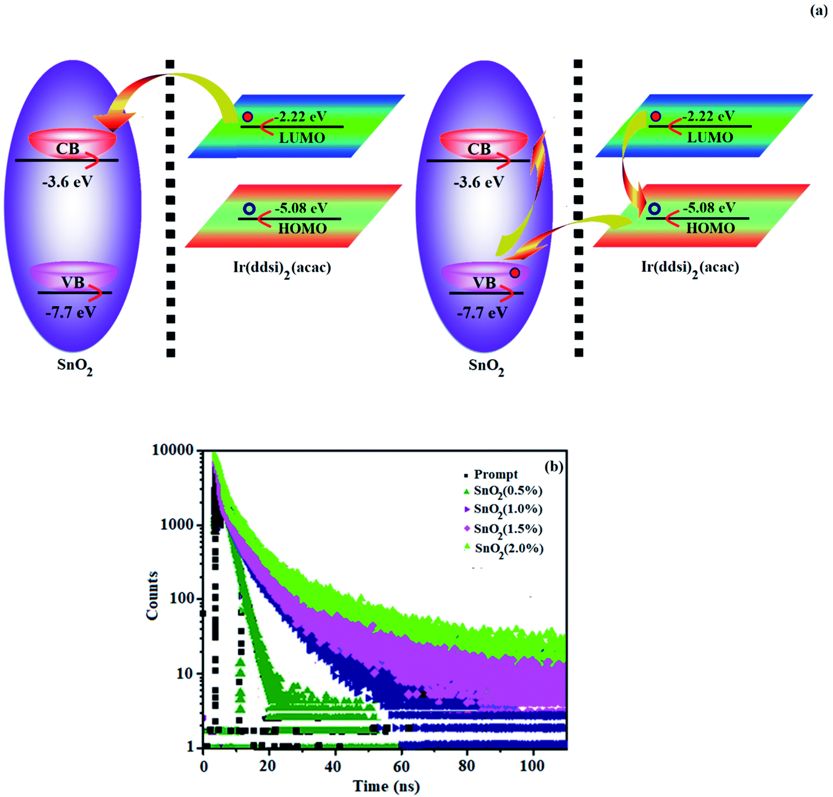
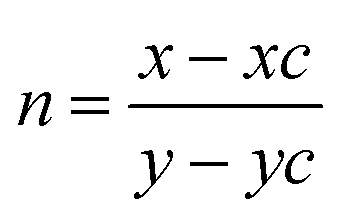
The thicknesses of 4.8 nm sized SnO2 NP layers spin-coated from 0.5, 1.0, 1.5 and 2.0 wt% solutions were 11, 13, 20 and 25 nm, respectively. The root-mean-square (RMS) roughness of the SnO2 NP layers spin-coated on ITO substrates from 0.5, 1.0, 1.5 and 2.0 wt% solutions are 2.96, 2.74, 2.51 and 2.13 nm, respectively (Fig. 2). The RMS roughness was much smoother than that of ITO (4.14 nm) and it decreased with increasing concentration of SnO2 NPs. Owing to the low-temperature (100 °C) thermal treatment, SnO2 NPs film retained an amorphous state, as shown in the XRD pattern. Hence, SnO2 NPs can be used as a functional layer at the interface between ITO and the ETL of OLEDs (Fig. 8). The lifetime of the film increased with an increasing thickness of the SnO2 NP layer (1.28 ns at 0%; 1.73 ns at 1.0%; 2.20 ns at 1.5% and 2.67 ns at 2.0%) (Fig. 7). The 2.0 wt% SnO2 NPs block exciton quenching efficiently by surface quenching or non-radiative energy transfer quenching mechanisms (Fig. 7). The electroluminescent performances of the fabricated devices using EIL SnO2 NPs with thicknesses of 2.96 (0.5 wt%), 2.74 (1.0 wt%), 2.51 (1.5 wt%), and 2.13 nm (2.0 wt%) were studied. The efficiencies of the devices fabricated by the combination of SnO2 NPs as EILs and green emissive material Ir(ddsi)2(acac) (devices I–IV) increased relative to the reference devices VI (0% SnO2) and VII [0% Ir(ddsi)2(acac)] (Fig. 8). Among devices II–V, device IV (with 2.0% SnO2; 25 nm) exhibited the maximum (SnO2 NPs/ITO) current efficiency (ηc, cd A−1: 52.3/24.3), power efficiency (ηp, lm W−1: 10.9/3.4), external quantum efficiency (ηex, %: 16.4/7.5) and luminance (L, cd m−2: 28182/1982). The reference devices VI (0% SnO2 NPs) and VII [Alq3(EML)] show luminances (L) of 1982 cd m−2 at 19.0 V and 2102 cd m−2 at 22.0 V, respectively. The enhanced efficiency with increasing SnO2 NP thickness may due to the fact that increasing the uniform surface coverage will increase the electron injection through improved energy level matching at the ITO:3TPYMB interface.74 As more electrons are injected, the e−–h+ balance is improved, leading to enhanced efficiencies over those of other devices.
 |
| | Fig. 7 (a) Exciton dissociation SnO2:Ir(ddsi)2(acac) interface and non-radiative energy transfer from Ir(ddsi)2(acac) to SnO2 NPs and (b) lifetime decay of devices. | |
 |
| | Fig. 8 Device performances: (a) current density and voltage; (b) current efficiency and current density; (c) power efficiency and current density; (d) external quantum efficiency and current density; and (e) normalized electroluminescent spectra of devices (I–V) (inset: CIE – V). | |
The electron injection barrier (1.48 eV) from ITO to the ELUMO of 3TPYMB is reduced (0.28 eV) to 1.2 eV using an SnO2 NP layer. The device with 2.0 wt% SnO2 NPs shows enhanced efficiencies: ηc, cd A−1 of 115%; ηp, lm W−1 of 221%; ηex, % of 119; ηL, cd m−2 767 times higher than the control device (without an SnO2 layer – device V). The device with 2.0 wt% SnO2 NPs shows enhanced efficiencies: ηc, cd A−1 of 396%; ηp, lm W−1 of 3966%; ηex, % of 466; ηL, cd m−2 766.9 times higher than the control device (Alq3 – device VI; see Table 2 and Fig. 8). As more electrons are injected into the ETL in the devices with an SnO2 NP layer, electron–hole recombination is enhanced and thus efficiencies are higher than those of the control device. Comparing the performances of IBOLEDs with different SnO2 layer thicknesses, a higher efficiency has been harvested in the device with a thicker SnO2 film. This is attributed to the smoother surface morphology of the SnO2 film in a thicker film. The normalized EL spectra of devices I–V show emission at 504 nm for IBOLEDs without a change in the shape of the emission peak, since the layer is highly transparent (Fig. 8). The SnO2 NP layer scarcely affects the EL spectra of IBOLEDs because the layer is highly transparent and amorphous.
Table 2 Summary of device efficiencies of SnO2(I–IV) and Cd–SnO2(V) with control devices
| Device (% SnO2(I–IV) & Cd–SnO2(V)) |
V1000 (V) |
La (cd m−2) |
ɳexb (%) |
ɳcc (cd A−) |
ɳpe (lm W−1) |
Zɳp(VI/VII)f (%) |
Zɳex(VI/VII)g (%) |
Zɳc(VI/VII)h (%) |
ZɳL(VI/VII)i (%) |
| Brightness. Maximum external quantum efficiency. Luminous efficiency. Power efficiency. Zηp = (ηpi – ηp/ηp) × 100. Zηex = (ηexi - ηex/ηex) × 100. Zηc = [ηci − ηc/ηc) × 100. ZnL = (Li − L/L) × 100. Values for devices with NPs. ITO/SnO2 (2.0%)/Alq3 (100 nm)/MoO3 (10 nm)/Al (100 nm). VII [Alq3(EML)]. |
| I (0.5%)d |
16.8 |
14215 |
14.8 |
43.0 |
7.5 |
121/241 |
97/412 |
77/1287 |
617/576 |
| I (1.0%)d |
16.6 |
15710 |
15.9 |
45.2 |
7.9 |
132/249 |
112/450 |
82/1326 |
693/647 |
| III (1.5%)d |
16.6 |
16631 |
16.0 |
50.4 |
10.2 |
200/364 |
113/454 |
107/1526 |
739/691 |
| IV (2.0%)d |
15.1 |
28182 |
16.4 |
52.3 |
10.9 |
221/396 |
119/466 |
115/1587 |
767/767 |
| V (2.0%)d |
13.3 |
30858 |
18.3 |
60.6 |
15.4 |
352/432 |
144/533 |
144/533 |
1255/1178 |
| Control device VI (0%)j |
19.0 |
1982 |
7.5 |
24.3 |
3.4 |
— |
— |
— |
— |
| Control device (VII)k |
22.0 |
2102 |
3.1 |
2.2 |
2.89 |
— |
— |
— |
— |
We have also fabricated devices using Cd–SnO2 as an electron injection layer. The device with a 2.0% Cd-doped SnO2 layer shows higher current efficiency ηc (60.6 cd A−1) and power efficiency ηp (15.4 lm W−1) than those of devices I–IV (Fig. 8 and 9). These higher efficiencies reveal that the Cd-doped SnO2 layer in combination with Ir(ddsi)2(acac) makes electron injection more efficient through the improved energy level matching at the ITO:Ir(ddsi)2(acac) interface. The current density and luminance increase as the concentration of Cd-doped SnO2 increases, because the total thickness of the device increases. As the thickness of the Cd-doped SnO2 layer increases to 4.0%, the current density and luminance increase slightly. This may be due to the fact that the injection and transport of electrons become better than those of organic molecules, as the surface coverage of Cd-doped SnO2 on ITO becomes better with an increase in the Cd-doped SnO2 layer thickness.75–77 A systematic study for device optimization by controlling the thickness and morphology of Cd-doped SnO2 is under way. Therefore the use of a Cd-doped SnO2 layer in an optoelectronic device is of current interest owing to the advantages of processability at low temperature, surface roughness and photostability. The device with 2.0 wt% Cd-doped SnO2 shows enhanced efficiencies: ηc, cd A−1 of 115/1587%; ηp, lm W−1 of 221/396%; ηex, % of 119/466; ηL, cd m−2 767/767 times higher than those of control devices (VI/V).
 |
| | Fig. 9 Device configuration with energy level diagram of HyLEDs. | |
The band gap energy of CdO is much lower (2.24 eV) than that of SnO2 (4.1 eV) and this may be the reason for the effective performances of Cd2+ doped SnO2 as an electron injection material. The lowering of the band gap results in a lowering of the ECB of Cd-doped SnO2 and promotes electron injection from ITO to the ECB of Cd–SnO2, leading to enhanced device performance. The Cd-doped SnO2 layer injects electrons efficiently due to the improved energy level matching at the ITO:Cd-doped SnO2:Ir(ddsi)2(acac) interface. As more electrons are injected, effective electron–hole recombination leads to higher efficiencies than that of the control device. Holes are injected from the Au anode coated with MoO3 HIL into the highest occupied molecular orbital (HOMO) of Ir(ddsi)2(acac) and electrons are injected from the Cd-doped SnO2–EIL-coated ITO cathode into the LUMO of Ir(ddsi)2(acac). The CB of Cd-doped SnO2 is situated higher than the LUMO of the emissive material Ir(ddsi)2(acac), which leads to activation-less electron injection from Cd–SnO2 into Ir(ddsi)2(acac). The deeper VB of Cd-doped SnO2 results in an efficient hole-blocking functionality, improving efficiencies78 (Table 2). The efficiencies of SnO2 and Cd-doped SnO2 based devices have been compared with those of various recently reported electron injection layers (Table S1†)78,79 which shows that SnO2 and Cd-doped SnO2 based devices are the best in terms of power and current efficiencies, and we believe that SnO2 and Cd-doped SnO2 NPs should be adopted as good potential candidates for future displays as well as for device performance.
The EL spectrum of Cd-doped SnO2 (λex = 380 nm) shows a broad yellow emission centered at 580 nm which is similar to the PL spectra with a red-shift in the emission peak position due to increase in excitation wavelength. In addition to the broad yellow emission at 580 nm, weak blue emission at 401 nm also appears in the EL spectra. This blue emission may be attributed to tin interstitials and non-stoichiometric oxides, which encouraged us to check the white emission.80 In order to obtain white emission, Cd-doped SnO2NPs are mixed with homoleptic blue phosphor Ir(tsi)3 (1:4). The blended phosphors are excited by a 380 nm LED chip driven at an applied voltage of 2.8 V and 3.5 mA current. The recorded EL spectrum shows yellow emission at 568 nm with weak blue emission at 428 nm originating from blue phosphor Ir(tsi)3. The combined emission of blue and yellow phosphors leads to white emission with CIE (0.31, 0.30) and CCT = 6961 K. White emission is classified as warm or cold in terms of CCT (correlated color temperature) values, calculated using the McCamy empirical formula:81 CCT = −449n3 + 352n2 − 6823n + 5520.33, where  is the negative inverse slope of the line, xc = 0.332 and yc = 0.186, and the obtained CCT value is 6961 K. Generally, a CCT value greater than 5000 K implies a cold white light used for commercial lighting purposes and less than 5000 K indicates a warm white light used for home applications.47 In the present study, the CCT value is 6961 K, which represents cold white light emission. Thus, Cd-doped SnO2 nanoparticles could be a better replacement for the metal activator doped yellow phosphors used for white OLED fabrication.
3.5. White light emission from BMIMBF4–Cd–SnO2 colloidal electrolyte
We have synthesised hybrid colloidal electrolyte namely, BMIMBF4–Cd–SnO2 to generate white light emission upon photoexcitation of BMIMBF4–Cd–SnO2, BMIMBF4 ionic liquid show emission at 450 nm may attributed to associated form of BMIMBF4 ionic liquid.81 In Cd-doped SnO2 NPs, some O2− ions escape from host lattice, leading to the formation of oxygen vacancies. This oxygen vacancy centre can trap an electron, resulting in the formation of defect states.81 The valence band (VB), defect states and conduction band (CB) are the three energy levels for Cd–SnO2 NPs. After the addition of Cd2+ to the host lattice, the negative charge of the Cd2+ ion has to be compensated for somewhere in the lattice in the form of an oxygen vacancy. By incorporating Cd2+ ions into the SnO2 host, metastable V0 centers are created in situ, which will share electrons from nearby tin vacancies to present the form of a tin–oxygen vacancy pair and luminescence intensity is increased compared to pristine SnO2 due to the simultaneous formation of V0 centers. However, after introducing Cd2+ ions into the host, non-radiative recombination can also occur easily due to the enhanced probability of the interaction with nearby Cd2+ ions, originating from the continuous solubility of Cd2+ ions in the SnO2 host. The surface effects can strongly influence the optical properties of these SnO2 nanoparticles. Because of the large surface-to-volume ratio of SnO2 nanoparticles, much unsaturated bonding of the surface atoms is expected at the surface of the particles. So, the surface will play an important role in the quenching of the luminescence. Recombination of holes in this centre with electrons in the CB leads to trap emissions at 492 nm (green) and at 572 nm (yellow).81 Photo-excitation of the BMIMBF4–Cd–SnO2 hybrid electrolyte exhibits strong emission at 450 nm, 492 nm and 572 nm. A combination of blue emission from BMIMBF4 and green and yellow emissions from Cd–SnO2NPs generates intense white light with CIE (0.34, 0.35) and CCT = 5188 K (Fig. 10).
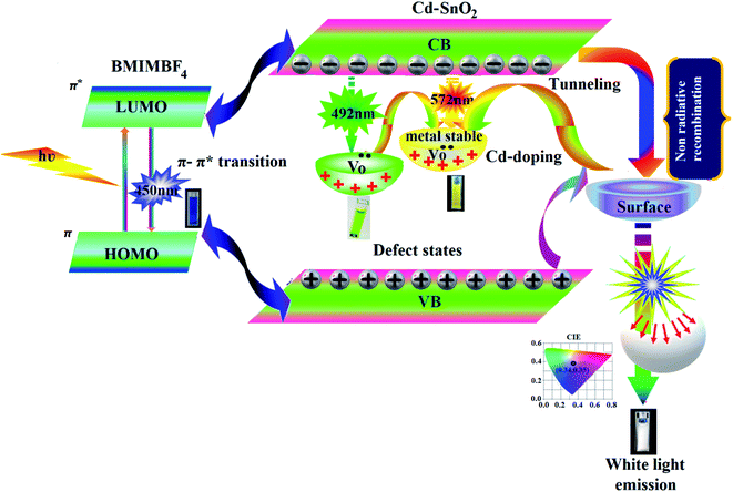 |
| | Fig. 10 White light generation from BMIMBF4–Cd–SnO2 colloidal hybrid electrolyte. | |
4. Conclusion
Enhanced efficiencies have been harvested from IBOLEDs using electron injection layer SnO2 NPs and/or Cd–SnO2 NPs coated at the ITO:ETL interface. The 2.0% SnO2 NPs (25 nm) with Ir(ddsi)2(acac) emissive material enhance efficiencies (SnO2/ITO), current efficiency (ηc, cd A−1: 52.3/24.3), power efficiency (ηp, lm W−1: 10.9/3.4), external quantum efficiency (ηex, %: 16.4/7.5) and luminance (L, cd m−2: 28182/1982). The device with a 2.0% Cd-doped SnO2 layer shows a higher ηc (60.6 cd A−1), ηp (15.4 lmW−1), ηex (18.3%) and L (26858 cd m−2) at 2.36 V than SnO2 devices or control devices. White light has been generated from a mixture of Cd–SnO2 NPs and homoleptic blue phosphor Ir(tsi)3. A combination of blue emission (λEL = 428 nm) from Ir(tsi)3 and defect emission from Cd–SnO2 NPs (λEL = 568 nm) gives intense white light with CIE (0.31, 0.30) and CCT = 6961 K. Upon photo-excitation, BMIMBF4–Cd–SnO2 gives white emission with CIE (0.34, 0.35) and CCT = 5188 K by the combination of blue and yellow emissions.
Conflicts of interest
There are no conflicts to declare.
Acknowledgements
This research was supported by the DST (Department of Science and Technology – EMR/2014/000094, F. No. SR/S1/1C-73/2010, F. No. SR/S1/1C-07/2007), DRDO (Defence Research and Development Organization – 213/MAT/10-11), CSIR (Council of Scientific and Industrial Research – No. 01/(2707)/13EMR-II), UGC (University Grant Commission – 6-21/2008, F. No. 30-71/2004(SR)) and DST-Nano Mission (SR/NM/NS-1001/2016).
References
- C. W. Han, K. M. Kim, S. J. Bae, H. S. Choi, J. M. Lee, T. S. Kim, Y. H. Tak, S. Y. Cha and B. C. Ahn, SID Int. - Symp. Dig. Tech. Pap., 2012, 43, 279–281 CrossRef
 .
. - R. Reineke, F. Lindner, G. Schwartz, N. Seidler, K. Walzer, B. Lüssem and K. Leo, Nature, 2009, 459, 234–238 CrossRef .
- K. Yamae, H. Tsuji, V. Kittichungchit, Y. Matsuhisa, S. Hayashi, N. Ide and Y. Komoda, SID Int. - Symp. Dig. Tech. Pap., 2012, 43, 694–697 CrossRef .
- T. Y. Chu, J. F. Chen and C. H. Chen, Jpn. J. Appl. Phys., 2006, 45, 4948–4950 CrossRef CAS .
- X. Zhou, M. Pfeiffer, J. S. Huang, J. Blochwitz-Nimoth, D. S. Qin, A. Werner, J. Drechsel, B. Maenning and K. Leo, Appl. Phys. Lett., 2002, 81, 922–924 CrossRef CAS .
- T. Y. Chu, J. F. Chen, S. Y. Chen, C. J. Chen and C. H. Chen, Appl. Phys. Lett., 2006, 89, 053503–053508 CrossRef .
- S. Y. Chen, T. Y. Chu, J. F. Chen, C. Y. Su and C. H. Chen, Appl. Phys. Lett., 2006, 89, 053518–053521 CrossRef .
- T. Xiong, F. Wang, X. Qiao and D. Ma, Appl. Phys. Lett., 2008, 92, 263305–263308 CrossRef .
- J. H. Lee, P. S. Wang, H. D. Park, C. I. Wu and J. J. Kim, Org. Electron., 2011, 12, 1763–1767 CrossRef CAS .
- B. W. D'Andrade, S. R. Forrest and A. B. Chwang, Appl. Phys. Lett., 2003, 83, 3858–3860 CrossRef .
- G. Parthasarathy, C. Shen, A. Kahn and S. R. Forrest, J. Appl. Phys., 2001, 89, 4986–4992 CrossRef CAS .
- C. Zhong, S. Liu, F. Huang, H. Wu and Y. Cao, Chem. Mater., 2011, 23, 4870–4876 CrossRef CAS .
- M. Sessolo and H. J. Bolink, Adv. Mater., 2011, 23, 1829–1845 CrossRef CAS PubMed .
- Y. Vaynzof, D. Kabra, T. J. K. Brenner, H. Sirringhaus and R. H. Friend, Isr. J. Chem., 2012, 52, 496–517 CrossRef CAS .
- M. G. Panthani and B. A. Korgel, Annu. Rev. Chem. Biomol. Eng., 2012, 3, 287–311 CrossRef CAS .
- D. Kabra, L. P. Lu, M. H. Song, H. J. Snaith and R. H. Friend, Adv. Mater., 2010, 22, 3194–3198 CrossRef CAS PubMed .
- J. W. Ryan, E. Palomares and E. Martínez-Ferrero, J. Mater. Chem., 2011, 21, 4774–4777 RSC .
- H. J. Bolink, E. Coronado, D. Repetto, M. Sessolo, E. M. Barea, J. Bisquert, G. Garcia-Belmonte, J. Prochazka and L. Kavan, Adv. Funct. Mater., 2008, 18, 145–150 CrossRef CAS .
- N. Tokmoldin, N. Griffiths, D. D. C. Bradley and S. A. Haque, Adv. Mater., 2009, 21, 3475–3478 CrossRef CAS .
- T. Chiba, Y. J. Pu, M. Hirasawa, A. Masuhara, H. Sasabe and J. Kido, ACS Appl. Mater. Interfaces, 2012, 4, 6104–6108 CrossRef CAS PubMed .
- T. Chiba, Y. J. Pu, H. Sasabe, J. Kido and Y. Yang, J. Mater. Chem., 2012, 22, 22769–22773 RSC .
- S. Y. Ryu, S. H. Kim, C. S. Kim, S. Jo and J. Y. Lee, Curr. Appl. Phys., 2012, 12, 1378–1380 CrossRef .
- H. Lee, I. Park, J. Kwak, D. Y. Yoon and C. Lee, Appl. Phys. Lett., 2010, 96, 153306–153309 CrossRef .
- L. Qian, Y. Zheng, K. R. Choudhury, D. Bera, F. So, J. Xue and P. H. Holloway, Nano Today, 2010, 5, 384–389 CrossRef CAS .
- J. Kwak, W. K. Bae, D. Lee, I. Park, J. Lim, M. Park, H. Cho, H. Woo, D. Y. Yoon, K. Char, S. Lee and C. Lee, Nano Lett., 2012, 12, 2362–2366 CrossRef CAS PubMed .
- T. Kuwabara, C. Tamai, Y. Omura, T. Yamaguchi, T. Taima and K. Takahashi, Org. Electron., 2013, 14, 649–656 CrossRef CAS .
- A. Kay and M. Grätzel, Chem. Mater., 2002, 14, 2930–2935 CrossRef CAS .
- J. M. Caruge, J. E. Halpert, V. Wood, V. Bulović and M. G. Bawendi, Nat. Photon., 2008, 2, 247–250 CrossRef CAS .
- S. Sadhu, T. Sen and A. Patra, Chem. Phys. Lett., 2007, 440, 121–124 CrossRef CAS .
- S. C. Vanithakumari and K. K. Nanda, Adv. Mater., 2009, 21, 3581–3584 CrossRef CAS .
- F. Wang, Y. H. Chen, C. Y. Liu and D. G. Ma, Chem. Commun., 2011, 47, 3502–3504 RSC .
- K. S. Sanju, P. P. Neelakandan and D. Ramaiah, Chem. Commun., 2011, 47, 1288–1290 RSC .
- V. Vohra, G. Calzaferri, S. Destri, M. Pasini, W. Porzio and C. Botta, ACS Nano, 2010, 4, 1409–1416 CrossRef CAS PubMed .
- X. Wang, W. Li and K. Sun, J. Mater. Chem., 2011, 21, 8558–8565 RSC .
- P. Kumar, L. S. Panchakarla, S. V. Bhat, U. Maitra, K. S. Subrahmanyam and C. N. R. Rao, Nanotechnology, 2010, 21, 385701–385706 CrossRef .
- S. Ye, F. Xiao, Y. X. Pan, Y. Y. Ma and Q. Y. Zhang, Mater. Sci. Eng. Rep., 2010, 71, 1–34 CrossRef .
- C. H. Huang and T. M. Chen, Opt. Express, 2010, 18, 5089–5099 CrossRef CAS PubMed .
- A. Kar, S. Kundu and A. Patra, J. Phys. Chem. C, 2011, 115, 118–124 CrossRef CAS .
- Z. Lia, X. Lia, X. Zhanga and Y. Qian, J. Cryst. Growth, 2006, 291, 258–261 CrossRef .
- P. P. Sahay, R. K. Mishra, S. N. Pandey, S. Jha and M. Shamsuddin, Curr. Appl. Phys., 2013, 13, 479–486 CrossRef .
- M. G. Tecedor, D. Maestre, A. Cremades and J. Piqueras, J. Mater. Chem. C, 2016, 4, 5709–5716 RSC .
- G. Godinho, A. Walsh and G. W. Watson, J. Phys. Chem. C, 2009, 113, 439–448 CrossRef .
-
(a) M. J. Frisch, G. W. Trucks, H. B. Schlegel, G. E. Scuseria, M. A. Robb, J. R. Cheeseman, G. Scalmani, V. Barone, B. Mennucci, G. A. Petersson, H. Nakatsuji, M. Caricato, X. Li, H. P. Hratchian, A. F. Izmaylov, J. Bloino, G. Zheng, J. L. Sonnenberg, M. Hada, M. Ehara, K. Toyota, R. Fukuda, J. Hasegawa, M. Ishida, T. Nakajima, Y. Honda, O. Kitao, H. Nakai, T. Vreven, J. A. Montgomery, J. E. Peralta, F. Ogliaro, M. Bearpark, J. J. Heyd, E. Brothers, K. N. Kudin, V. N. Staroverov, R. Kobayashi, J. Normand, K. Raghavachari, A. Rendell, J. C. Burant, S. S. Iyengar, J. Tomasi, M. Cossi, N. Rega, J. M. Millam, M. Klene, J. E. Knox, J. B. Cross, V. Bakken, C. Adamo, J. Jaramillo, R. Gomperts, R. E. Stratmann, O. Yazyev, A. J. Austin, R. Cammi, C. Pomelli, J. W. Ochterski, R. L. Martin, K. Morokuma, V. G. Zakrzewski, G. A. Voth, P. Salvador, J. J. Dannenberg, S. Dapprich, A. D. Daniels, O. Farkas, J. B. Foresman, J. V. Ortiz, J. Cioslowski, and D. J. Fox, Gaussian, Inc., Wallingford., CT, 2009, vol. 121, pp. 150–166 ;
(b) T. Lu and F. Chen, J. Comput. Chem., 2012, 33, 580–592 CrossRef CAS PubMed .
- S. Gnanam and V. Rajendran, J. Sol-Gel Sci. Technol., 2010, 53, 555–559 CrossRef CAS .
- X. Liu, J. Iqbal, Z. Wu, B. He and R. Yu, J. Phys. Chem. C, 2010, 114, 4790–4796 CrossRef CAS .
- V. Vasanthia, M. Kottaisamy, K. Anitha and V. Ramakrishnan, Mater. Sci. Semicond. Process., 2018, 85, 141–149 CrossRef .
- R. Mariappan, V. Ponnuswamy, P. Suresh, R. Suresh, M. Ragavendar and C. Sankar, Mater. Sci. Semicond. Process., 2013, 16, 825–832 CrossRef CAS .
- V. Kumar, V. Kumar, S. Som, J. H. Neethling, E. Olivier, O. M. Ntwaeaborwa and H. C. Swart, Nanotechnology, 2014, 25, 135701–135710 CrossRef PubMed .
- G. Zhang, C. Xie, S. Zhang, S. Zhang and Y. Xiong, J. Phys. Chem. C, 2014, 118, 18097–18109 CrossRef CAS .
- J. D. Prades, J. Arbiol, A. Cirera, J. R. Morante, M. Avella, L. Zanotti, E. Comini, G. Faglia and G. Sberveglieri, Sens. Actuators, B, 2007, 126, 6–12 CrossRef CAS .
- S. Samson and C. G. Fonstad, J. Appl. Phys., 1973, 44, 4618–4621 CrossRef CAS .
- S. Lettieri, M. Causa, A. Setaro, F. Trani, V. Barone, D. Ninno and P. Maddalena, J. Chem. Phys., 2008, 129, 244710–244714 CrossRef CAS PubMed .
- B. X. Mi, P. F. Wang, M. W. Liu, H. L. Kwong, N. B. Wong, C. S. Lee and S. T. Lee, Chem. Mater., 2003, 15, 3148–3151 CrossRef CAS .
- J. D. Priest, G. Y. Zheng, N. Goswami, D. M. Eichhorn, C. Woods and D. P. Rillema, Inorg. Chem., 2000, 39, 1955–1963 CrossRef PubMed .
- J. Jayabharathi, V. Thanikachalam, K. Saravanan and N. Srinivasan, J. Fluoresc., 2011, 21, 507–519 CrossRef CAS PubMed .
- K. Saravanan, N. Srinivasan, V. Thanikachalam and J. Jayabharathi, J. Fluoresc., 2011, 21, 65–80 CrossRef CAS PubMed .
- J. Jayabharathi, V. Thanikachalam, N. Srinivasan and K. Saravanan, J. Fluoresc., 2011, 21, 596–606 Search PubMed .
- J. Jayabharathi, V. Thanikachalam and K. Saravanan, J. Photochem. Photobiol., A, 2009, 208, 13–20 CrossRef CAS .
- S. Lamansky, P. Djurovich, D. Murphy, F. Abdel Razzaq, H. F. Lee, C. Adachi, P. E. Burrows, S. R. Forrest and M. E. Thompson, J. Am. Chem. Soc., 2001, 123, 4304–4312 CrossRef CAS PubMed .
- M. G. Colombo, A. Hauser and H. U. Gudel, Inorg. Chem., 1993, 32, 3088–3092 CrossRef CAS .
- S. Okada, K. Okinaka, H. Iwawaki, M. Furugori, M. Hashimoto, T. Mukaide, J. Kamatani, S. Igawa, A. Tsuboyama, T. Takiguchi and K. Ueno, Dalton Trans., 2005, 9, 1583–1590 RSC .
- K. C. Tang, K. L. Liu and I. C. Chen, Chem. Phys. Lett., 2004, 386, 437–441 CrossRef CAS .
-
(a) D. S. Mcclure, J. Chem. Phys., 1949, 17, 905–913 CrossRef CAS ;
(b) W. L. Leong, P. S. Lee, S. G. Mhaisalkar, T. P. Chen and A. Dodabalapur, Appl. Phys. Lett., 2007, 90, 042906–042910 CrossRef .
- H. Bassler and B. Schweitzer, Acc. Chem. Res., 1999, 32, 173–182 CrossRef .
- N. J. Turro, V. Ramamurthy and J. C. Scaiano, ChemPhysChem, 2012, 88, 1033–1036 Search PubMed .
- C. K. Moon, K. H. Kim, J. W. Lee and J. J. Kim, Chem. Mater., 2015, 27, 2767–2769 CrossRef CAS .
- H. Jou, Y. X. Lin, S. H. Peng, C. J. Li, Y. M. Yang, C. L. Chin, J. J. Shyue, S. S. Sun, M. Lee, C. T. Chen, M. C. Liu, C. C. Chen, G. Y. Chen, J. H. Wu, C. H. Li, C. F. Sung, M. J. Lee and J. P. Hu, Adv. Mater., 2014, 26, 555–562 Search PubMed .
- R. S. Kesarkar, W. Mróz, M. Penconi, M. Pasini, S. Destri, M. Cazzaniga, D. Ceresoli, P. R. Mussini, C. Baldoli, U. Giovanella and A. Bossi, Angew. Chem., 2016, 128, 2764–2768 CrossRef .
- L. S. Cui, Y. Liu, X. Y. Liu, Z. Q. Jiang and L. S. Liao, ACS Appl. Mater. Interfaces, 2015, 7, 11007–11014 CrossRef CAS PubMed .
-
(a) J. Liu, Z. Zeng, X. Cao, G. Lu, L. H. Wang, Q. L. Fan, W. Huang and H. Zhang, Small, 2012, 8, 3517–3522 CrossRef CAS PubMed ;
(b) Z. Wang, Y. Feng, S. Zhang, Y. Gao, Z. Gao, Y. Chen, X. Zhang, P. Lu, B. Yang, P. Chen, Y. Mab and S. Liuc, Phys. Chem. Chem. Phys., 2014, 16, 20772–20779 RSC .
- M. Lepeltier, F. M. Savary, B. Graff, J. Lalevée, D. Gigmes and F. Dumur, Synth. Met., 2015, 199, 139–146 CrossRef CAS .
- X. Yang, X. Xu, J. S. Dang, G. Zhou, C. L. Ho and W. Y. Wong, Inorg. Chem., 2016, 55, 1720–1727 CrossRef CAS .
- D. R. Martir, A. K. Bansal, V. D. Mascio, D. B. Cordes, A. F. Henwood, A. M. Z. Slawin, P. C. J. Kamer, L. M. Sarti, A. Pertegás, H. J. Bolink, I. D. W. Samuel and E. Z. Colman, Inorg. Chem. Front., 2016, 3, 218–235 RSC .
- J. B. Baxter and C. A. Schmuttenmaer, J. Phys. Chem. B, 2006, 110, 25229–25239 CrossRef CAS PubMed .
- S. K. Hau, H. L. Yip, N. S. Baek, J. Zou, K. O'Malley and A. K. Y. Jen, Appl. Phys. Lett., 2008, 92, 253301–253304 CrossRef .
- B. S. Ong, C. Li, Y. Li, Y. Wu and R. Loutfy, J. Am. Chem. Soc., 2007, 129, 2750–2751 CrossRef CAS PubMed .
- J. B. Baxter and C. A. Schmuttenmaer, J. Phys. Chem. B, 2006, 110, 25229–25239 CrossRef CAS PubMed .
- S. Stolz, Y. Zhang, U. Lemmer, G. H. Sosa and H. Aziz, ACS Appl. Mater. Interfaces, 2017, 9, 2776–2785 CrossRef CAS .
- J. Jayabharathi, S. Panimozhi, V. Thanikachalam, A. Prabhakaran and P. Jeeva, RSC Adv., 2018, 8, 8402–8411 RSC .
- S. S. Changa, S. O. Yoona and H. J. Park, Ceram. Int., 2005, 31, 405–410 CrossRef .
-
(a) J. Jhon, M. Vequizo, S. Kamimura, T. Ohno and A. Yamakata, Phys. Chem. Chem. Phys., 2018, 20, 3241–3248 RSC ;
(b) A. Mele, C. D. Tran and S. H. P. Lacerda, Angew. Chem., Int. Ed., 2003, 42, 4364–4366 CrossRef CAS PubMed ;
(c) H. Hamaguchi and R. Ozawa, Adv. Chem. Phys., 2005, 131, 85–104 CrossRef CAS ;
(d) H. Tokuda, K. Hayamizu, K. Ishii, M. A. B. H. Susan and M. Watanabe, J. Phys. Chem. B, 2004, 108, 16593–16600 CrossRef CAS ;
(e) C. S. McCamy, Color Res. Appl., 1992, 17, 142–144 CrossRef .
Footnote |
| † Electronic supplementary information (ESI) available. See DOI: 10.1039/d0ra02122a |
|
| This journal is © The Royal Society of Chemistry 2020 |
Click here to see how this site uses Cookies. View our privacy policy here. 
 Open Access Article
 This Open Access Article is licensed under a Creative Commons Attribution-Non Commercial 3.0 Unported Licence
 ,
Balu Seransenguttuvan and
Jayaraman Jayabharathi
,
Balu Seransenguttuvan and
Jayaraman Jayabharathi
 , where ϕunk and ϕstd are the radiative quantum yield of the sample and standard; Iunk and Istd are the integrated emission intensities of sample and standard, respectively; Aunk and Astd are the absorbance of sample and standard, respectively; and ηunk and ηstd are the refractive index of sample and standard solution, respectively. The solid-state quantum yield was measured on a quartz plate with an integrating sphere.


 , where S is the Huang–Rhys factor, correlated to the intensities of vibration from the excited 3MLCT/3π–π* state to the ground state (S0),
 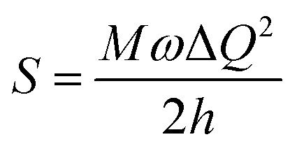 ; ω is the vibrational frequency, M is the reduced mass, and ΔQ is the displacement of potential energy surfaces between the S0 and excited states. The structural distortion upon excitation is explained by the ratio of the height of the two emission peaks
 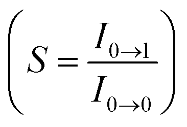 .
.


 is the negative inverse slope of the line, xc = 0.332 and yc = 0.186, and the obtained CCT value is 6961 K. Generally, a CCT value greater than 5000 K implies a cold white light used for commercial lighting purposes and less than 5000 K indicates a warm white light used for home applications.47 In the present study, the CCT value is 6961 K, which represents cold white light emission. Thus, Cd-doped SnO2 nanoparticles could be a better replacement for the metal activator doped yellow phosphors used for white OLED fabrication.