DOI:
10.1039/D0RA01756F
(Paper)
RSC Adv., 2020,
10, 16404-16414
Highly transparent phototransistor based on quantum-dots and ZnO bilayers for optical logic gate operation in visible-light†
Received
24th February 2020
, Accepted 8th April 2020
First published on 24th April 2020
Abstract
Highly transparent optical logic circuits operated with visible light signals are fabricated using phototransistors with a heterostructure comprised of an oxide semiconductor (ZnO) with a wide bandgap and quantum dots (CdSe/ZnS QDs) with a small bandgap. ZnO serves as a highly transparent active channel, while the QDs absorb visible light and generate photoexcited charge carriers. The induced charge carriers can then be injected into the ZnO conduction band from the QD conduction band, which enables current to flow to activate the phototransistor. The photoexcited charge transfer mechanism is investigated using time-resolved photoluminescence spectroscopy, scanning Kelvin probe microscopy, and ultraviolet photoelectron spectroscopy. Measurements show that carriers in the QD conduction band can transfer to the ZnO conduction band under visible light illumination due to a change in the Fermi energy level. Moreover, the barrier for electron injection into the ZnO conduction band from the QD conduction band is low enough to allow photocurrent generation in the QDs/ZnO phototransistor. Highly transparent NOT, NOR, and NAND optical logic circuits are fabricated using the QDs/ZnO heterostructure and transparent indium tin oxide electrodes. This work provides a means of developing highly transparent optical logic circuits that can operate under illumination with low-energy photons such as those found in visible light.
Introduction
Photosensors are considered essential for the complete development of the internet of things (IoT), because the IoT relies on observations of the surrounding environment.1–3 Optical logic circuits are receiving attention, because they can perform various functions in response to light signals.4 To perform optical logic operations for the IoT using light signals, photosensors should be developed to selectively detect ultraviolet (UV), visible, or infrared (IR) light. The most important light sources emit wavelengths in the visible region, as most of the information about environmental surroundings is contained in this wavelength range.5 Visible light communication (VLC) technology has rapidly emerged with the development of optical wireless communication for the IoT. VLC with visible light-emitting diodes (LEDs) can be used for highly secure indoor communication in spaces that are sensitive to interference from electromagnetic waves, such as aircraft cabins and hospitals. VLC systems operated with visible LEDs must detect light in the visible region. This means that the photosensors and optical logic circuits in VLC controllers must efficiently detect light in the visible region.6–8 However, nontransparent Si-based visible light sensors are not suitable for next-generation technology, which is expected to employ transparent electronics. New, highly transparent visible light photosensors and optical logic circuits should thus be developed.
Highly transparent and large-scale visible light photosensors are required for high-performance next-generation IoT technology.9 Visible light photosensors are typically fabricated using silicon, because the Si bandgap is small enough to absorb light over the entire visible spectrum. However, it is difficult to fabricate transparent visible light photosensors using silicon, since its bandgap is too small to be transparent.10 It is also difficult to realize large-scale optoelectronics based on silicon technology.11 Several highly transparent and large-scale visible light photosensors have recently been fabricated via a solution-based method using a combination of an oxide semiconductor and nanoparticles.12–14 The most useful devices for realizing highly transparent and large-scale visible light photosensors are phototransistors based on oxide semiconductors with wide bandgaps and quantum dots (QDs) with small bandgaps.15 The wide bandgap of the oxide semiconductor provides a transparent active channel for the device, while the QDs with a small bandgap absorb visible light and generate photoelectrons that are injected into the conduction band of the oxide semiconductor.16 Colloidal QDs are considered as a promising semiconducting materials for optoelectronics, because their bandgaps can be tuned by controlling the dimensions of the QDs.17,18 Colloidal QDs can be manufactured at low cost using a solution-based process and adapted for large-scale optoelectronics.19 Although the development of highly transparent visible light phototransistors based on oxide semiconductors and QDs has been explored, few attempts have been made to properly investigate the origin of photocurrents in hybrid oxide semiconductor-QD structures.20 In addition, it is difficult to find reports in which the operation of highly transparent optical logic circuits with visible light signals is examined.
In this study, we developed a highly transparent phototransistor that could convert visible light into a photocurrent using an oxide semiconductor (ZnO) and colloidal CdSe/ZnS QDs heterojunction layer. Ultraviolet photoelectron spectroscopy (UPS), time-resolved photoluminescence (TRPL) spectroscopy, and scanning Kelvin probe microscopy (SKPM) were used to investigate the origin and behavior of photoexcited carriers at the interface between the oxide semiconductor and the QDs. We performed a detailed investigation of the interfacial energy band diagram and changes in the Fermi energy level under visible light illumination. The TRPL measurements indicated that the induced photoexcited carriers in the QDs were injected into the conduction band of the oxide semiconductor. In addition, highly transparent NOT, NOR, and NAND optical logic circuits were constructed by combining the highly transparent phototransistors, which has the heterostructure of oxide semiconductor and QDs. The highly transparent optical logic circuits successfully performed functional operations in response to visible light signals.
Results and discussion
Fig. 1a shows a three-dimensional phototransistor on a glass substrate under illumination with visible light. The device channel had a highly transparent heterostructure comprised of quantum dots (CdSe/ZnS QDs) and zinc oxide (ZnO). Transparent aluminum oxide (Al2O3) served as the gate dielectric of the device.21 The measured capacitance of Al2O3 was 175 nF cm−2 (Fig. S1 in the ESI†). The bottom gate, source electrode, and drain electrode were composed of transparent indium tin oxide (ITO). A cross-sectional transmission electron microscope (TEM) image of the phototransistor is shown in Fig. 1b. The thickness of the QDs/ZnO photoactive channel was 40 nm, while that of the Al2O3 layer was 100 nm. The absorption spectra of ZnO and QDs/ZnO films on glass substrates are shown in Fig. 1c. The QDs/ZnO spectrum indicated it absorbed light at λ = 635 nm, while absorption of light in the visible region by the ZnO film was not significant. Since QDs were formed a thin layer on ZnO with an annealing process, the observed peak was weak compared to the peak of QDs solution.16,22 The spectra of both the QDs/ZnO film and the QDs solution contained absorption peaks at 635 nm (Fig. S2†). The transmittance spectra of the photoactive channel region and the electrode region are shown in Fig. 1d. The photoactive channel region was composed of ITO/Al2O3/QDs/ZnO on a glass substrate, while the electrode region above the ZnO layer consisted of additional ITO with a thickness of 100 nm. The transmittance of the photoactive channel region at 550 nm was 95%. The average transmittance of light in the visible region from 400 to 700 nm near the source and drain electrodes was 82.5%. The bandgaps of ZnO and the QDs were 3.35 eV and 1.92 eV, respectively, as shown in the Tauc plots in Fig. S3.† Although the device could absorb light at a wavelength of 635 nm, transmittance in the visible region was high due to the wide bandgap of ZnO and the thinness of the QD layer.23 A photograph of the highly transparent phototransistor is shown in Fig. 1e.
 |
| | Fig. 1 (a) Schematic diagram of a highly transparent phototransistor on a glass substrate with a ZnO and QDs active channel heterostructure. (b) Cross-sectional TEM image of the phototransistor. (c) UV/vis absorption spectra of the ZnO and QDs/ZnO films. The spectrum of the QDs/ZnO film is shown in detail in the inset. (d) Transmittance spectra of the highly transparent phototransistors. (e) Photograph of a fabricated phototransistor with a QDs/ZnO heterostructure and ITO electrodes. | |
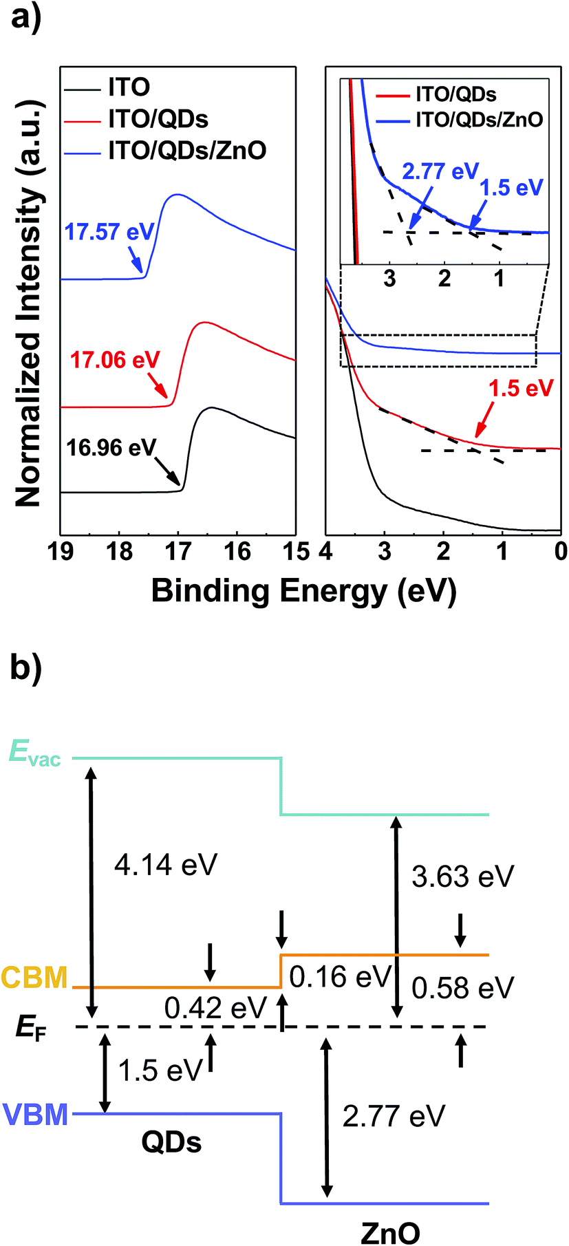
UPS measurements were performed to investigate the electronic structure of the interface between the QDs and ZnO. The secondary electron cutoff (SEC) regions and the highest occupied molecular orbitals (HOMOs) of the ITO, ITO/QDs, and ITO/QDs/ZnO films are shown in Fig. 2a. The work function of ITO could be calculated by considering its SEC and incident energy from the UV source (21.2 eV). The ITO work function was 4.24 eV, and the calculated distances between the vacuum (Evac) levels and the Fermi energy (EF) levels of the QDs and ZnO were 4.14 and 3.63 eV, respectively. The measured valence band maximum (VBM) of the QDs on ITO was 1.5 eV from the EF, while the measured VBM of ZnO was 2.77 eV. This is shown in the HOMO region in the inset of Fig. 2a. The energy band diagram of the interface between the QDs and ZnO is depicted in Fig. 2b. The conduction band minimum (CBM) was obtained from the Tauc plots of the QD and ZnO absorbance spectra (Fig. S3†). Based on the Tauc plots, the calculated optical bandgaps of the QDs and ZnO were 1.92 and 3.35 eV, respectively.24,25 The CBMs of the QDs and ZnO were thus 0.42 eV and 0.58 eV above the EF, respectively. Notably, the barrier for electron injection into the CBM of ZnO from the CBM of the QDs was 0.16 eV. This meant that electrons in the CBM of the QDs could be injected into the CBM of ZnO with slight excitation by a small external field or energy from illuminating photons.26
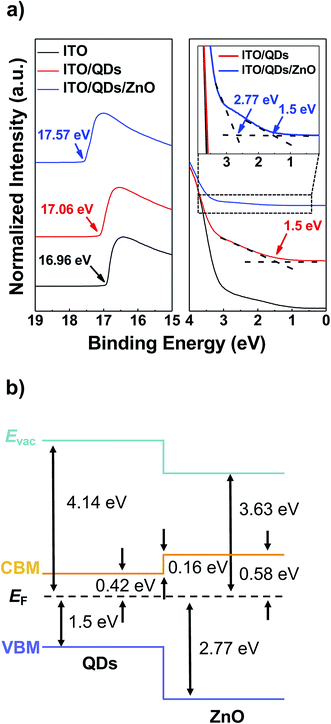 |
| | Fig. 2 (a) UPS spectra of ITO, ITO/QDs, and ITO/QDs/ZnO in the SEC and HOMO regions. The spectrum of ITO/QDs/ZnO in the HOMO region is shown in the inset. (b) Interfacial energy band diagrams of the QDs and ZnO. | |
The electrical characteristics of the fabricated ZnO thin-film transistor (TFT) and QDs/ZnO TFT without external light illumination are shown in Fig. 3a and b. The output curves and structures of the ZnO TFT and QDs/ZnO TFT devices are shown in the insets. Typical ZnO TFT transfer curves were recorded at an applied drain voltage (VD) of 5 V. The calculated field effect mobility was 0.746 cm2 V−1 s−1, and the on/off ratio was ∼107. In contrast, the field effect mobility of the QDs/ZnO TFT was 0.02 cm2 V−1 s−1, and its on/off ratio was ∼106. The reduced field effect mobility and on/off ratio of the QDs/ZnO TFT could have originated from roughness at the interface between ZnO and Al2O3 due to the interfacial QDs, as shown in the inset of Fig. 3b. Transfer curves were recorded with the prepared devices under illumination at wavelengths from 405 to 780 nm to investigate their photoresponse characteristics. The transfer curves of the ZnO TFT are shown in Fig. 3c and d shows the QDs/ZnO TFT transfer curves under illumination at various wavelengths. Increases in the drain current (ID) were difficult to detect at wavelengths of 520, 635, and 780 nm, since the photon energies at these wavelengths were not sufficient to overcome the ZnO bandgap. An increase of the ID in the on/off region of the device and a negative shift in the threshold voltage (VTH) were observed under illumination at 405 nm due to the higher photon energy. There was no increase in ID in the negative VG region under illumination at 450 nm, since the photon energy (2.763 eV) was smaller than the ZnO bandgap (3.35 eV). Although the photon energy at 450 nm was smaller than the ZnO bandgap, a negative shift in VTH was observed along with a photocurrent in the device in the on state. The increase in ID in the on state and the negative shift in VTH with insufficient energy (λ = 450 nm) could have originated from a defect in the solution-processed ZnO film or the Urbach tail, which was observed in the absorption spectrum of a typical ZnO film (Fig. S3†). Ionized oxygen vacancies in the deep and mid-gap levels of ZnO may have also caused unexpected photocarrier generation with insufficient photon energy.23,27 A remarkable increase in the photocurrent was observed under visible light illumination when QDs were present between ZnO and Al2O3, as shown in Fig. 3d. Due to the small QD bandgap (1.92 eV), the device could generate a photocurrent under illumination with visible light (λ = 450, 520, and 635 nm). The photon energy was sufficient to promote electrons from the valence band into the conduction band of the QDs. The photoexcited carriers could then be promoted into the ZnO conduction band by an external field, such as a small drain voltage (VD).16,20 However, it was difficult to induce a photocurrent under illumination at 780 nm, because the photon energy was smaller than the bandgaps of the QDs and ZnO (Fig. 3d).
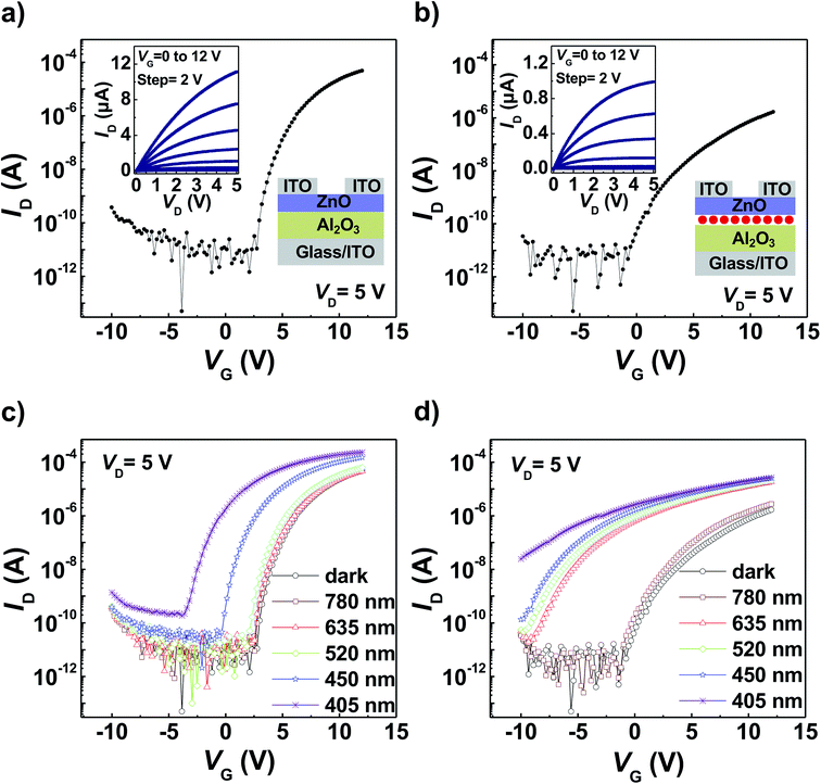 |
| | Fig. 3 Transfer curves of (a) the ZnO TFT and (b) the QDs/ZnO TFT without light exposure. The output curves and structures of ZnO and the QDs/ZnO TFT devices are shown in the insets. Transfer curves of (c) the ZnO TFT and (d) the QDs/ZnO TFT devices under illumination at various wavelengths at a power of 4.5 mW cm−2. | |
The photoresponsivity of the ZnO and QDs/ZnO phototransistors under various illumination conditions were calculated using equation:
Itotal is the total current in the device;
Idark is the dark current;
P is the power of the incident light;
Apt is the product of channel width and thickness;
Apd is the spot size of the laser source;
Jph is the photocurrent density; and
P is the incident laser power density.
28 Photoresponsivity is shown as a function of illumination in
Fig. 4a. The photoresponsivities were calculated at
VG = −5 V and
VD = 5 V and an illumination power of 4.5 mW cm
−2. The photoresponsivity of the ZnO TFT was negligible under illumination at
λ = 405, 450, 520, and 635 nm. In contrast, the photoresponsivity of the QDs/ZnO TFT increased in the visible light range. The calculated photoresponsivity of the QDs/ZnO TFT under illumination at 405, 450, 520, and 635 nm were 10.7, 0.873, 0.801, and 0.142 mA W
−1, respectively. The photoresponsivity of the QDs/ZnO TFT under visible light was sufficiently high for it to be used as a visible light photoswitching device. Photomodulation of the device was measured while applying a periodic light signal at 1 Hz and a
VG of −5 V.
Fig. 4b shows the photomodulation of the ZnO TFT with periodic light signals with wavelengths of 405 and 635 nm. The device did not respond to illumination with low-energy photons (
λ = 635 nm) due to the wide bandgap of ZnO. However, the ZnO TFT could be photomodulated under periodic illumination at
λ = 405 nm, which was consistent with the data shown in
Fig. 3c. The QDs/ZnO TFT exhibited photomodulation upon exposure to a periodic signal at 635 nm, as shown in
Fig. 4c. The small bandgap of the QDs clearly helped generate a photocurrent in the device under illumination with visible light. Therefore, the QDs/ZnO TFT could be turned on and off using a periodic on/off signal at 635 nm. However, the device did not respond to illumination at 780 nm, since the photon energy was smaller than the bandgap of the QDs.
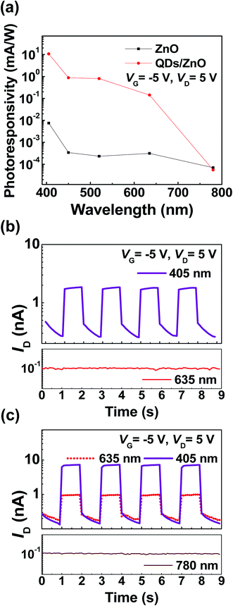 |
| | Fig. 4 (a) Photoresponsivity of the ZnO TFT and QDs/ZnO TFT as a function of illumination wavelength. Photomodulation of (b) the ZnO TFT and (c) the QDs/ZnO TFT under periodic illumination with light (λ = 405, 635, and 780 nm). | |
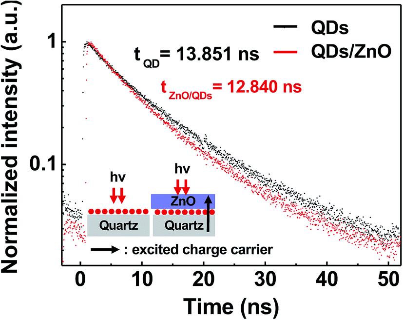
To clarify the mechanism of photoexcited carrier transfer between the QDs and ZnO, TRPL spectroscopy was performed to investigate the exciton decay dynamics (Fig. 5) using a time-correlated single photon counting (TCSPC) system. We prepared samples from QD and QDs/ZnO films on quartz substrates. The two samples were excited with a 375 nm pulsed laser, and TRPL decay profiles were recorded at 620 nm. The transient photoluminescence (PL) decay curves were fitted using the linear sum of multiple exponential decay model,  . In the model, ai is the weighting coefficient of the exponential, and τi is the corresponding decay time. The weighted average of the characteristic times, 〈τ〉, was calculated using equation:
| 〈τ〉 = (a1τ12 + a2τ22 + …)/(a1τ1 + a2τ2 + …) |
 |
| | Fig. 5 Time-resolved photoluminescence (TRPL) measurements of QDs and QDs/ZnO films on quartz substrates. The measurements are illustrated schematically in the inset. | |
The curve was fitted using i values of 1 and 2, which provided reasonable fits to the parameters shown in Table 1.29,30 To simplify the analysis, curve fitting was performed for biexponential decay (i = 1, 2), which contained non-radiative decay (a1, t1) and radiative decay (a2, t2) values. Radiative decay usually occurs when photons are absorbed. In contrast, non-radiative decay proceeds through various routes that do not involve absorption, such as quenching and vibration. The PL decay profiles of the QD and QDs/ZnO films showed biexponential decay on a time scale of a few tens of nanoseconds. However, the QDs/ZnO film had a shorter average decay time (〈τ〉 = 12.84 ns) than the QD film (〈τ〉 = 13.851 ns). This phenomenon was related to quenching, which occurred at the QDs/ZnO interface via effective charge carrier transfer from the QDs to ZnO.20,31,32 The decay behaviors of the QD and QDs/ZnO films also differed in background intensity at negative times, which showed the times before 0 ns when the sample was exposed by the excitation pulse. This difference may have been caused by a local excess of carriers, which did not undergo recombination in the QDs.33 This suggested that transfer of the carriers from the QDs to ZnO was possible due to quenching effect. To further study carrier transitions in our QD and QDs/ZnO films, we compared the transition rates determined from the TRPL data (Table 2). The transition rate can be calculated from the average decay time using equation:
which corresponds to the number of charge carrier transitions per unit of time. The QDs/ZnO film had a transition rate (1/
t) of 0.20724 ns
−1, which was higher than that of the QD film (1/
t = 0.19372 ns
−1). These results confirmed that the ZnO film facilitated the effective transfer of charge carriers from the QDs to ZnO. Therefore, the TRPL measurements indicated that charge carriers could be generated through the separation of excitons in the QDs by incident visible light photons and transferred into the ZnO.
Table 1 Fitting coefficients and average lifetimes of the QD and QDs/ZnO films determined through TRPL decay analysis
| |
a1 |
t1 [ns] |
a2 |
t2 [ns] |
Decay average time 〈τ〉 [ns] |
| QDs |
0.73801 |
6.9045 |
0.26199 |
20.4571 |
13.851 |
| QDs/ZnO |
0.80755 |
6.2601 |
0.19245 |
21.052 |
12.840 |
Table 2 Transition rates of the QD and QDs/ZnO films determined through TRPL decay analysis
| |
1/t1 [ns−1] |
1/t2 [ns−1] |
Transition rate (t−1) [ns−1] |
| QDs |
0.14483 |
0.04888 |
0.19372 |
| QDs/ZnO |
0.15974 |
0.0475 |
0.20724 |
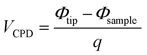
To investigate the origin of the photoinduced current between the QDs and ZnO under illumination with visible light (Fig. 3d), SKPM was performed to measure changes in the surface potential with changes in EF under illumination. The sample was fixed on a copper plate, and the work function of the NCST–Au tip (4.85 eV) was calibrated using a highly oriented pyrolytic graphite (HOPG) substrate. The sample was grounded on the copper plate, and AC voltage with an amplitude of 0.5–1 V was applied to the SKPM tip at a frequency of 17 kHz during measurement. The relative contact potential difference (VCPD) of the ZnO, QDs, and QDs/ZnO surfaces with respect to the SKPM tip were measured in an ambient atmosphere in the presence and absence of illumination with 635 nm light. The measured VCPD between the sample and the tip could be calculated using equation:
Φtip and
Φsample are the work functions of the tip and sample, respectively, and
q is the electric charge.
34 Fig. 6a shows the
VCPD of the ZnO surface on ITO with and without illumination at 635 nm. Δ
VCPD on the ZnO surface was negligible, because the illuminating light could not excite electrons from the valence band to the conduction band of ZnO. However, the measured Δ
VCPD of the QDs on ITO with and without illumination was 130 mV (
Fig. 6b). Δ
VCPD of the QDs was closely related to the photoexcited electrons in the QD valence band. Excited electrons from the QD valence band accumulated in the conduction band, and the surface potential could then be modulated.
33,35,36 The
VCPD of the QDs/ZnO surface on ITO also increased under illumination at 635 nm, as shown in
Fig. 6c (Δ
VCPD = 108 mV). The surface topography profiles with and without illumination and schematic diagrams of the films are shown in the insets. Based on the measured Δ
VCPD values of 108 mV on QDs/ZnO and 130 mV on the QDs, photoexcited electrons could be injected into ZnO from the QDs by reducing Δ
VCPD to approximately 22 mV with a change in
EF.
33,37 Changes in the interfacial energy band diagrams of the QDs and ZnO in the off state of the device with and without illumination at 635 nm are shown schematically in
Fig. 6d. Generally,
EF is strongly related to the number of electrons in the conduction band. Without illumination, the conduction band of the QDs was nearly empty. However, the QD conduction band contained plentiful photoexcited electrons under illumination with visible light, even when the device was turned off (
Fig. 6d). The increase in the number of photoexcited electrons in the conduction band shifted the
EF upward towards the conduction band. Δ
EF was approximately 0.130 eV, which made the QDs resemble a highly doped n-type semiconductor. Accumulated electrons in the QD conduction band could then transfer to the ZnO conduction band. This suggested that an upward shift in the
EF of the QDs towards the conduction band made it possible for photoexcited carriers to be transferred from the QDs to ZnO by overcoming the barrier potential between the QDs and ZnO. Therefore, photoexcitation of electrons with visible light and reduction of the QDs and ZnO surface potential difference with a highly doped n-type semiconductor to change the
EF could induce a photocurrent from the QDs to ZnO, even when the device was turned off (
VTH <
VG) (
Fig. 3d). A schematic diagram showing the working mechanism of the device under illumination at 635 nm when
VG <
VTH is shown in
Fig. 6e. Although the active channel of ZnO was depleted when
VG <
VTH, photoexcited carriers could induce a photocurrent in the channel (
Fig. 6d). In this case, photocurrent was generated only through the photoexcitation of carriers in the QDs by visible light. A schematic diagram showing the working mechanism of the device under illumination at 635 nm when
VG >
VTH is shown in
Fig. 6f. When
VG >
VTH, the ZnO channel contained an accumulation region with its own current. When the device was illuminated with visible light, additional photoexcited carriers could be injected into the ZnO conduction band from the QDs. Therefore, a significant increase in the current was observed when
VG >
VTH, as shown in
Fig. 3d. The SKPM measurements revealed the origin of the increased current under illumination with visible light when the device was either on or off. The SKPM measurements provided direct evidence of the origin of photoexcited carriers and the dynamics between QDs and ZnO.
 |
| | Fig. 6 VCPD measurements of (a) ITO/ZnO and (b) ITO/QDs. (c) ITO/QDs/ZnO films with and without illumination at 635 nm. The topography profiles are shown in the insets. (d) Schematic interfacial energy band diagrams of the QDs and ZnO in darkness and during exposure to light. Schematic illustration of photocurrent channel formation in the device under illumination at λ = 635 nm when (e) VG < VTH (off state) and (f) VG > VTH (on state). | |
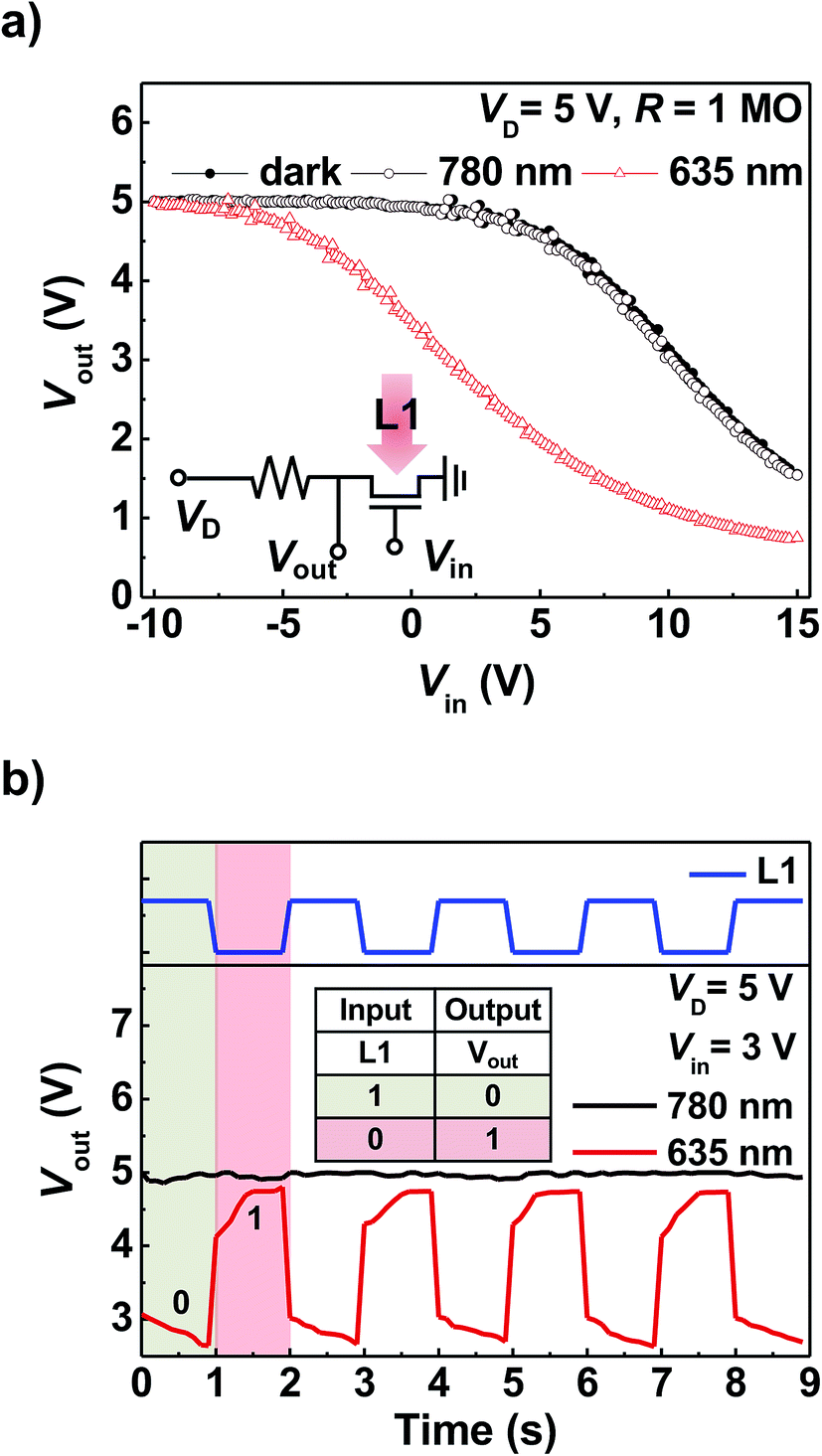
To further investigate the application of photocurrent on the QDs/ZnO TFT under illumination with visible light, highly transparent optical logic circuits were fabricated to perform functional operations in response to visible light signals. Fig. 7a shows the output voltage (Vout) of the photoinverter circuit (NOT gate) as a function of the input voltage (Vin). A circuit diagram including the QDs/ZnO TFT and a load resistance of 1 MΩ is shown in the inset. Without illumination, Vin − Vout behavior characteristic of an inverter circuit was observed. The Vin − Vout curve did not change when the active region of the QDs/ZnO TFT was exposed to light at λ = 780 nm, since the photon energy was not sufficient to generate a photocurrent. However, when the device was illuminated at λ = 635 nm, a negative shift in the Vin − Vout curve was observed due to photocurrent generation in the QD/ZnO TFT. Therefore, the circuit could perform a NOT gate functional operation. Photomodulation of the NOT gate circuit was performed using a periodic light signal (L1) with a frequency of 1 Hz at VD = 5 V and Vin = 3 V (Fig. 7b). A truth table for the functional operation of the optical NOT gate circuit is shown in the inset. The periodic response of the circuit corresponded to the periodic visible light signal. The circuit did not respond to a periodic signal with a wavelength of 780 nm.
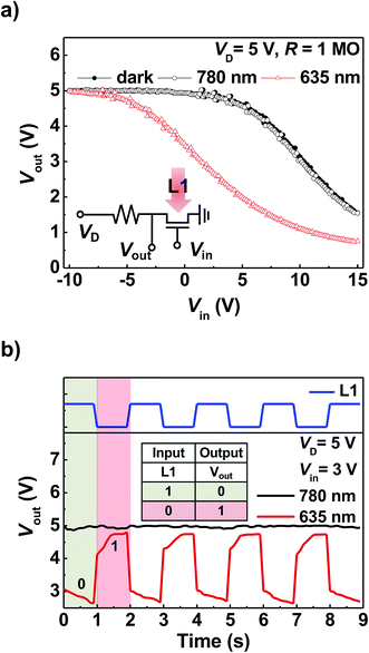 |
| | Fig. 7 (a) Photoinduced voltage characteristics of a photoinverter consisting of a QDs/ZnO TFT and a 1 MΩ load resistor with and without exposure to light at λ = 635 nm. The photoinverter circuit diagram is shown in the inset. (b) Photoswitching under periodic on/off light cycles at λ = 635 and 780 nm. A table of the input and output signals of the photoinverter circuit (NOT gate) is shown in the inset. The signal from the light source (L1) is indicated by the blue line. | |
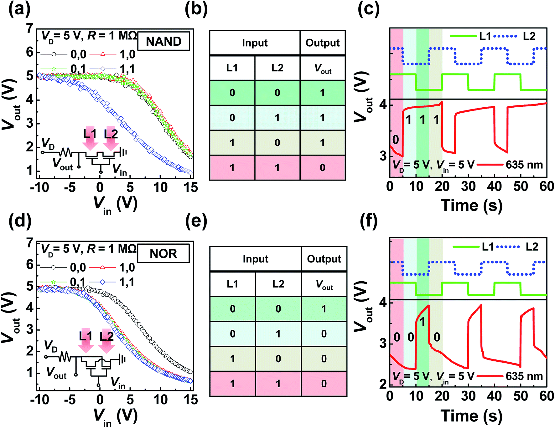
Highly transparent optical NAND and NOR gates composed of two QDs/ZnO TFTs could be controlled through input from two visible light-pulse signals with matching wavelengths at a load resistance of 1 MΩ. Fig. 8a shows the Vin − Vout curves of the optical NAND gate circuits on the QDs/ZnO TFTs under illumination with a visible light signal at 635 nm. A circuit diagram containing a NAND gate circuit is shown in the inset. When neither QDs/ZnO TFT was exposed to visible light, a typical Vin − Vout curve characteristic of an inverter circuit was observed. The Vin − Vout curve did not change when only one of the two QDs/ZnO TFT active channels was exposed to visible light, since the circuit was a NAND gate circuit. However, a negative shift in the Vin − Vout curve was observed when both QDs/ZnO TFTs were exposed to visible light simultaneously due to the generation of a photocurrent on both TFTs. The truth table is shown in Fig. 8b. In the truth table, an input value of 0 indicates the visible light signal is turned off, while an input value of 1 means the light signal for the QDs/ZnO TFTs is on. An output signal of 0 indicates the NAND circuit is off, and an output value of 1 means the circuit is on. Photomodulation of the NAND circuit is depicted in Fig. 8c. Two alternating visible light input pulses, L1 (green) and L2 (blue), are shown in the upper region of the Fig. 8c. The photomodulated output signal of the NAND circuit is shown in the lower portion of the graph. The Vin − Vout characteristics and photomodulation of the NAND circuit were consistent with the truth table in Fig. 8b. The Vin − Vout characteristics of the optical NOR gate circuits on the QDs/ZnO TFTs under illumination with visible light at 635 nm are shown in Fig. 8d. A circuit diagram containing an optical NOR gate circuit is shown in the inset. When neither QDs/ZnO TFT was exposed to visible light, the Vin − Vout characteristics of an inverter circuit were observed. However, a negative shift in the Vin − Vout curve was observed when one of the QDs/ZnO TFT active channels or both channels simultaneously were exposed to visible light due to the generation of photocurrent. The results are shown in the truth table in Fig. 8e. Photomodulation of the optical NOR circuit is illustrated in Fig. 8f. The two alternating visible light input pulses are shown in the upper region of the plot. The photomodulated output signal of the optical NOR circuit is shown in the lower area of the graph. The Vin − Vout characteristics and photomodulation of the NOR circuit were consistent with the truth table in Fig. 8d. These results indicate that highly transparent TFTs with QDs/ZnO heterojunctions can be basic components of highly transparent optical logic circuits that perform various functional operations under illumination with low-energy photons in visible light.
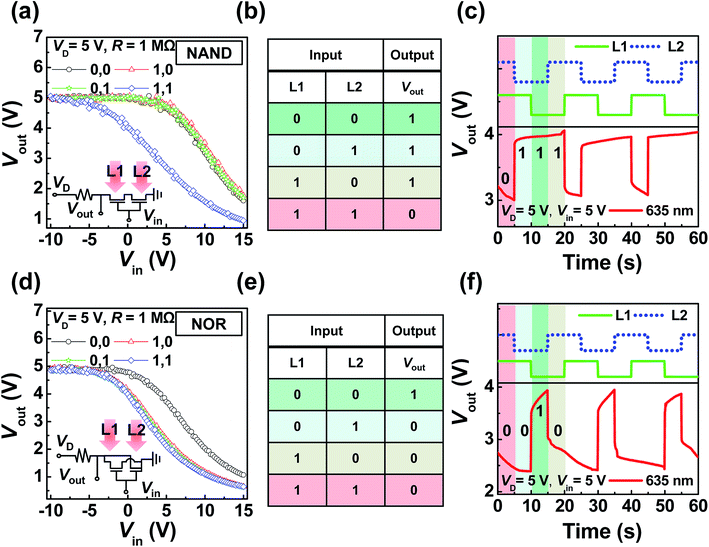 |
| | Fig. 8 (a) Photoinduced voltage characteristics of an optical NAND gate circuit consisting of two QDs/ZnO TFTs and a 1 MΩ load resistor with two light input signals. The optical NAND gate circuit diagram is shown in the inset. (b) Table of input and output signals of the optical NAND gate circuit. (c) Output voltage of the optical NAND gate circuit in response to two periodic on/off light signals at λ = 635 nm. (d) Photoinduced voltage characteristics of an optical NOR gate circuit with two light input signals. The optical NOR gate circuit diagram is shown in the inset. (e) Table of input and output signals of the optical NOR gate circuit. (f) Output voltage of the optical NOR gate circuit in response to two periodic on/off light signals at λ = 635 nm. The signal from light source 1 (L1) is indicated by the green line, and the signal from light source 2 (L2) is indicated by the blue dotted line. | |
Conclusions
We have demonstrated the operation of highly transparent optical logic circuits, which can perform various functional operations under illumination with visible light. The optical logic circuits were composed of TFTs with QDs/ZnO heterojunctions, in which ZnO with its wide bandgap served as a highly transparent active channel. The QDs, which had a smaller bandgap, enabled the absorption of visible light and generated photoexcited charge carriers that accumulated in the QD conduction band. The mechanism of photoexcited charge transfer between the QDs and ZnO was investigated using UPS, TRPL spectroscopy, and SKPM. Based on the interfacial energy band diagrams, we determined that the barrier for electron injection into the CBM of ZnO from the CBM of the QDs was 0.16 eV. This was small enough to allow the injection of electrons into the CBM of ZnO from the CBM of the QDs with little stimulation, such as that from a small external field or energy from illuminating photons. TRPL measurements indicated that charge carriers could be generated via the separation of excitons in the QDs by incident photons in visible light, and that the charge carriers could be transferred to the ZnO. Moreover, SKPM measurements revealed the origin of the current increase between the QDs and ZnO in the device in its on and off states under illumination with visible light. Highly transparent NOT, NOR, and NAND optical logic circuits were fabricated using the QDs/ZnO heterostructure and transparent ITO electrodes. Our findings provide a useful guide for developing highly transparent optoelectronic circuits, which can perform various functional operations under illumination with visible light for next-generation IoT technology.
Experimental
ZnO solution synthesis
A ZnO nanoparticle solution was obtained from a zinc amine precursor.16 The solution was prepared by mixing 0.0813 g ZnO powder (Sigma Aldrich, 99.999%) with 12 mL ammonium hydroxide (Alfa Aesar, 99.9%) and refrigerated for 5 h to increase the solubility of the ZnO powder.38
QDs solution synthesis
To fabricate a highly transparent phototransistor with a light response in the visible region, colloidal cadmium selenide/zinc sulfide (CdSe/ZnS) QDs (Plasmachem, PL-QD-O-630) were first dissolved in toluene to obtain a QD concentration of 5 mg mL−1. After that, the solution was kept near 0 °C. Typically, the size of visible light range of CdSe/ZnS QDs is ∼8 nm.39
Device fabrication
First, to improve the gate dielectric properties and transparency of the device, an Al2O3 gate dielectric layer was deposited onto a clean ITO (150 nm) glass substrate using an atomic layer deposition (ALD) system. ITO on a glass substrate was used as the gate electrode. QD films were spin-coated onto Al2O3 layer at 2000 rpm for 60 s, followed by annealing at 180 °C for 30 min. Then, ZnO films were deposited onto QDs surface using spin-coating process at 3000 rpm for 30 s. The ZnO film was then annealed at 180 °C for 1 h under ambient conditions to evaporated the solvent of ZnO. For the upper source/drain electrodes, a 100 nm-thick ITO layer was deposited onto the substrate via sputtering using a shadow mask. The channel length (L) and width (W) were 100 and 1000 μm, respectively. The sputtering system was operated at a low DC power of 27 W, and vacuum was maintained at 1 mTorr with an Ar flow rate of 24 sccm.
Characterization
A semiconductor parameter analyzer (HP 4145B) and a probe station were used to determine the optoelectrical characteristics of the device at an illumination power of approximately 4.5 mW cm−2. Absorbance by the hybrid films and transmittance through the device structure were measured using a UV/visible spectrometer (Jasco V-570) in darkness and under illumination with light at wavelengths (λ) of 405, 450, 520, 650, and 780 nm. To observe surface potential difference with respect to external photoexcitaion, Scanning Kelvin probe microscopy was performed by Park XE-7 system to measure changes in the surface potential using laser source (λ = 635 nm, power intensity = 4.5 mW cm−2). UPS measurements were used to analysis the electronic structure of the device with ultraviolet rays of 21.22 eV, the He–I line. TRPL spectroscopy was performed using a time-correlated single photon counting (TCSPC) system (Halcyone, Ultrafast systems) with a 375 nm pulsed laser for photoexcitation and TRPL decay profiles recorded at 620 nm. TEM measurements were used to analysis the device structure and thickness.
Conflicts of interest
There are no conflicts to declare.
Acknowledgements
This work was supported by LG Display under LGD-KHU incubation program.
Notes and references
- M. Ortiz, D. Hussein, S. Park, S. N. Han and N. Crespi, IEEE Internet of Things Journal, 2014, 1, 206 Search PubMed.
- J. Liu, G. Faulkner, B. Choubey, S. Collins and D. C. O' Brien, IEEE Sens. J., 2018, 18, 5321–5328 CAS.
- S. Saloni and A. Hegde, IEEE International Conference on Internet of Things and Applications, 2016, pp. 137–142 Search PubMed.
- Z. Y. Shen and L. L. Wu, Appl. Opt., 2008, 47, 3737–3742 CrossRef CAS PubMed.
- F. M. Wu, C. T. Lin, C. C. Wei, C. W. Chen, Z. Y. Chen, H. T. Huang and S. Chi, IEEE Photonics J., 2013, 5, 7901507 Search PubMed.
- K. Warmerdam, A. Pandharipande and D. Caicedo, IEEE Online Conference on Green Communications, 2015, pp. 47–52 Search PubMed.
- H. Ma, L. Lampe and S. Hranilovic, IEEE Trans. Commun., 2015, 63, 3313–3324 Search PubMed.
- T. Yamazato, I. Takai, H. Okada, T. Fujii, T. Yendo, S. Arai and S. Kawahito, IEEE Communications Magazine, 2014, 52, 88–97 Search PubMed.
- H. J. Song, M. H. Seo, K. W. Choi, M. S. Jo, J. Y. Yoo and J. B. Yoon, Sci. Rep., 2019, 9, 7334 CrossRef PubMed.
- C. Zhao, Z. Liang, M. Su, P. Liu, W. Mai and W. Xie, ACS Appl. Mater. Interfaces, 2015, 7, 25981–25990 CrossRef CAS PubMed.
- H. Chen, Y. Cao, J. Zhang and C. Zhou, Nat. Commun., 2014, 5, 4097 CrossRef CAS PubMed.
- S. Cha, S. Jeong, B. J. Kim, S. J. Kang, Y. D. Kim and I. K. Han, Curr. Appl. Phys., 2019, 19, 992–997 CrossRef.
- J. Yu, B. J. Kim, S. Park, I. K. Han and S. J. Kang, Jpn. J. Appl. Phys., 2018, 57, 044001 CrossRef.
- Y. Zhai, G. Chen, J. Ji, Z. Wu, Y. Li and Q. Wang, Phys. E, 2019, 113, 92–96 CrossRef CAS.
- S. W. Shin, K. H. Lee, J. S. Park and S. J. Kang, ACS Appl. Mater. Interfaces, 2015, 7, 19666–19671 CrossRef CAS PubMed.
- J. E. Cho, J. Yu and S. J. Kang, Curr. Appl. Phys., 2016, 16, 1560–1563 CrossRef.
- F. P. G. de Arquer, A. Armin, P. Meredith and E. H. Sargent, Nat. Rev. Mater., 2017, 2, 16100 CrossRef.
- X. Zhang, C. Hagglund and E. M. Johansson, Energy Environ. Sci., 2017, 10, 216–224 RSC.
- J. S. Park, J. Kyhm, H. H. Kim, S. Jeong, J. Kang, S. E. Lee and J. D. Song, Nano Lett., 2016, 16, 6946–6953 CrossRef CAS PubMed.
- D. K. Hwang, Y. T. Lee, H. S. Lee, Y. J. Lee, S. H. Shokouh, J. H. Kyhm, J. Lee, H. H. Kim, T. Yoo, S. H. Nam, D. I. Son, B. Ju, M. Park, J. D. Song, W. K. Choi and S. Im, NPG Asia Mater., 2016, 8, e233 CrossRef CAS.
- W. Xu, H. Wang, F. Xie, J. Chen, H. Cao and J. B. Xu, ACS Appl. Mater. Interfaces, 2015, 7, 5803–5810 CrossRef CAS PubMed.
- G. Wen, J. Fan, X. Li and Y. Liu, J. Non-Cryst. Solids, 2017, 463, 50–55 CrossRef CAS.
- Y. S. Rim, Y. Yang, S. H. Bae, H. Chen, C. Li, M. S. Goorsky and Y. Yang, Adv. Mater., 2015, 27, 6885–6891 CrossRef CAS PubMed.
- C. Y. Huang, T. S. Huang, C. Y. Cheng, Y. C. Cheng, Y. C. Chen, C. T. Wan, M. M. Rao and Y. K. Su, IEEE Photonics Technol. Lett., 2010, 22, 305–307 CAS.
- R. Rusdi, A. A. Rahman, N. S. Mohamed, N. Kamarudin and N. Kamarulzaman, Powder Technol., 2011, 210, 18–22 CrossRef CAS.
- S. M. Lee, S. J. Park, K. H. Lee, J. S. Park, S. Park, Y. Yi and S. J. Kang, Appl. Phys. Lett., 2015, 106, 031112 CrossRef.
- H. S. Kang, J. S. Kang, J. W. Kim and S. Y. Lee, J. Appl. Phys., 2004, 95, 1246–1250 CrossRef CAS.
- B. J. Kim, S. Park, S. K. Cha, I. K. Han and S. J. Kang, RSC Adv., 2018, 8, 23421–23425 RSC.
- X. W. Sun, J. Chen, J. L. Song, D. W. Zhao, W. Q. Deng and W. Lei, Opt. Express, 2010, 18, 1296–1301 CrossRef CAS PubMed.
- H. Wu, H. Si, Z. Zhang, Z. Kang, P. Wu, L. Zhou and Y. Zhang, Adv. Sci., 2018, 5, 1801219 CrossRef PubMed.
- K. S. Cho, K. Heo, C. W. Baik, J. Y. Choi, H. Jeong, S. Hwang and S. Y. Lee, Nat. Commun., 2017, 8, 840 CrossRef PubMed.
- C. Liu, K. Wang, C. Yi, X. Shi, P. Du, A. W. Smith and X. Gong, J. Mater. Chem. C, 2015, 3, 6600–6606 RSC.
- S. Jeong, J. Kyhm, S. K. Cha, D. K. Hwang, B. K. Ju, J. S. Park and I. K. Han, Small, 2019, 15, 1900008 CrossRef PubMed.
- J. Park, D. Bang, K. Jang, S. Haam, J. Yang and S. Na, Nanotechnology, 2012, 23, 365705 CrossRef PubMed.
- Y. Wang, Z. Xia, L. Liu, W. Xu, Z. Yuan, Y. Zhang and B. Sun, Adv. Mater., 2017, 29, 1606370 CrossRef PubMed.
- Q. Chen, F. Ye, J. Lai, P. Dai, S. Lu, C. Ma and L. Chen, Nano Energy, 2017, 40, 454–461 CrossRef CAS.
- V. W. Bergmann, S. A. Weber, F. J. Ramos, M. K. Nazeeruddin, M. Gratzel, D. Li and R. Berger, Nat. Commun., 2014, 5, 5001 CrossRef CAS PubMed.
- J. J. Richardson and F. F. Lange, Cryst. Growth Des., 2009, 9, 2570–2575 CrossRef CAS.
- M. Chaudhry, D.-K. Lim, R. Qamar and A. S. Bhatti, Phys. Chem. Chem. Phys., 2018, 20, 29446 RSC.
Footnotes |
| † Electronic supplementary information (ESI) available. See DOI: 10.1039/d0ra01756f |
| ‡ Authors contributed equally to this work. |
|
| This journal is © The Royal Society of Chemistry 2020 |
Click here to see how this site uses Cookies. View our privacy policy here. 
 Open Access Article
 This Open Access Article is licensed under a Creative Commons Attribution-Non Commercial 3.0 Unported Licence
 b,
Sungho Parka,
Shinyoung Jeongc,
Dohyeon Jeond,
Yebin Kangd,
Taekyeong Kimd,
Youn Sang Kim
b,
Sungho Parka,
Shinyoung Jeongc,
Dohyeon Jeond,
Yebin Kangd,
Taekyeong Kimd,
Youn Sang Kim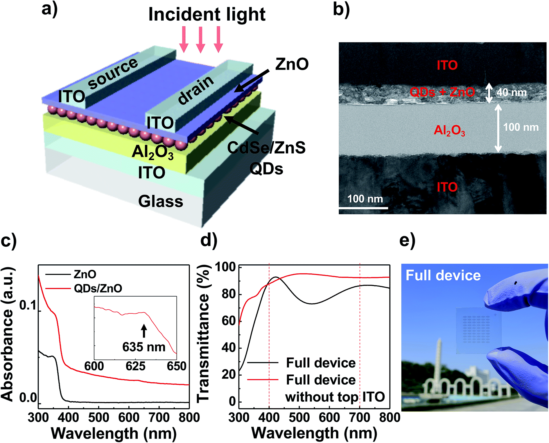


 . In the model, ai is the weighting coefficient of the exponential, and τi is the corresponding decay time. The weighted average of the characteristic times, 〈τ〉, was calculated using equation: