
 Open Access Article
 This Open Access Article is licensed under a Creative Commons Attribution-Non Commercial 3.0 Unported Licence
A novel method for in situ visualization of the growth kinetics, structures and behaviours of gas-phase fabricated metallic alloy nanoparticles†
Lei Zhang‡
a,
Long-Bing He‡ *ab,
Lei Shia,
Yu-Feng Yanga,
Guan-Lei Shanga,
Hua Honga and
Li-Tao Sun*ab
*ab,
Lei Shia,
Yu-Feng Yanga,
Guan-Lei Shanga,
Hua Honga and
Li-Tao Sun*ab
aSEU-FEI Nano-Pico Centre, Key Lab of MEMS of Ministry of Education, Southeast University, Nanjing 210096, P. R. China. E-mail: helongbing@seu.edu.cn
bCentre for Advanced Materials and Manufacture, Joint Research Institute of Southeast University and Monash University, Suzhou 215123, P. R. China
First published on 31st March 2020
Abstract
Modulation of gas-phase nanoparticles is unmethodical as there is a lack of information on the growth kinetics and its determinants. Here, we developed a novel in situ evaporation-and-deposition (EAD) method inside a transmission electron microscope which enables direct visualization of the nucleation, growth, coalescence and shape/phase evolution of gas-phase fabricated nanoparticles. Using a Bi49Pb18Sn12In21 alloy as a sample, the critical factors that determine the feasibility of this EAD method are revealed. By direct observation, it is unambiguously evidenced that pristine nanoparticles with ultra-clean surfaces are extremely energetic during growth. Coalescence between EAD-fabricated nanoparticles takes place in a manner beyond conventional understanding acquired by postmortem analyses. Moreover, the EAD-fabricated diverse nanoparticles show distinct size distributions and sandwich-type or Janus-type phase segregations. These features offer an effective tool to identify atomic surface steps of thin films and can provide an ideal case for exploring the phase diagrams of nanoalloys in the future.
Introduction
Nanoparticles are an important type of nanomaterial which opens the gate to a world of fantastic structures and novel properties.1–4 In the past two decades, it has been well realized that the novel properties of nanoparticles mostly originate from their size effect and large free surfaces.1,5–7 Therefore, researchers have spent great effort to develop fabrication methods to obtain nanoparticles with controllable size, shape, phase and elemental distribution.4,8–15 Among all the methods, chemical synthesis and gas-phase deposition are two outstanding ways as they show significant efficiency, controllability, and flexibility on the design and tuning of the nanoparticle structures. Although the chemical synthesis has gained big success in fabricating a large variety of functional nanoparticles with well-designed structures and morphologies, the use of surfactants frequently leads to a critical problem that the synthesized nanoparticles inevitably have organic molecules covered on the surfaces, largely weakening their activities in a lot of sensor applications.44,45 In contrast, the gas-phase fabricated nanoparticles usually have very clean surfaces due to the vacuum/inert fabrication conditions and the absence of organic surfactants.16,17 Also, the gas-phase fabrication methods are industrial compatible and easy to scale up. Unfortunately, the gas-phase fabrication methods usually have a weak ability to modulate the nanoparticle structures, phases and shapes.18–21 As a result, the gas-phase fabricated nanoparticles frequently show a randomly dispersed assembling,17,19,22 which goes against the expectation of enhanced collective properties. This issue seems to be more severe in the fabrication of alloy nanoparticles, as there is an abysmal lack of information about how they nucleate, grow, and alloying/segregating during the formation process.Unlike the chemical syntheses where liquid-cell transmission electron microscopy has provided a delicate way to deeply understand the growth dynamics in solutions,23–28 the case of gas-phase nanoparticles is rather ambiguous at present because neither the nucleation and growth processes during gas-phase preparation, nor the diffusion, migration, coalescence and ripening events after deposition are visible. Such powerlessness in realizing the formation dynamics of gas-phase nanoparticles usually leaves the nanoparticles and nanoparticle assemblies harsh and undesirable, causing unexpectable trouble in further device applications. In this paper, a novel method is developed to provide a visible way to probe into the aforementioned issues. Local heating and a large temperature gradient are created on a micro-sized alloy particle to enable in situ evaporation and deposition inside a transmission electron microscope (TEM). The dynamic formation and growth processes of nanoparticles are thus observed and recorded directly, shedding penetrating insights into the kinetics of gas-phase nucleation, growth, and ripening.
Results and discussion
Fig. 1a shows the illustration of the in situ evaporation-and-deposition (EAD) method. Basically, there are three key factors that determine the feasibility of this EAD method, that is, the intensity of the used electron beam (e-beam) which governs the input energy, the material type and size of the micro-ball which determine the amount of received energy and its conversion to heat, and the thermal conductivity of the substrate which determines the heat dissipation. In fact, these three factors frequently interact with each other, and some nanoparticles can be easily fabricated in a quite tolerant condition. An outstanding feature of this EAD method is that it can create a high-temperature gradient at the microscale, enabling the nucleation and re-deposition of the evaporated free atoms to form multifarious clusters and nanoparticles. Such an advantage affords an opportunity to have both the evaporation/sublimation process and the growth behaviours in the same view. Bi49Pb18Sn12In21 alloy is selected as the mother material to verify this EAD method because it has a low melting point and enables the testing of low-beam-intensity conditions during normal TEM characterization. The multiple elements in the mother alloy also provide an opportunity to investigate the size-dependent phase evolutions in pristine gas-phase deposited nanoparticles. Fig. 1b shows the obtained nanoparticles by using this EAD method with a Bi49Pb18Sn12In21 micro-ball. The inset shows the initial morphology of the alloy micro-ball fabricated by ultrasonication (see details in the Experimental part). After EAD, the micro-ball shrinks visibly as a portion of its mass has turned into alloy nanoparticles surrounding it. This EAD process has a strong significance differing from the Coulomb explosion observed previous,29–32 i.e. EAD growth process is consecutive and quite controllable instead of random bursts.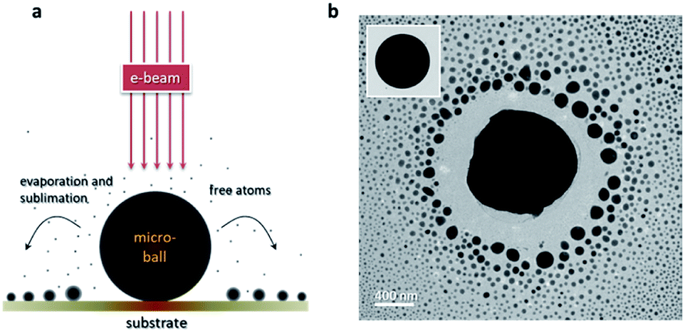 | ||
| Fig. 1 (a) Schematic illustration of the in situ EAD method. (b) Morphology of the alloy nanoparticles formed by the in situ EAD method. The inset shows the initial micro-ball before e-beam irradiation. | ||
Fig. 2 shows the influences of beam intensity and micro-ball size on the validity of the EAD method. Interestingly, for Bi49Pb18Sn12In21 micro-balls supported on thin-carbon films, the EAD phenomenon can hardly be achieved on those samples with a diameter smaller than around 500 nm, even a strong beam intensity of 105 A m−2 is used. For micro-balls with diameter from 500 nm to around 1 μm, very weak EAD phenomena are observed. In this case, only a few nanoparticles are formed during continuous irradiation, and no significant body shrinkage is observed. In sharp contrast, for those samples with a diameter larger than around 1 μm, drastic EAD phenomena in which diverse newly formed nanoparticles surrounding the micro-ball are observed. In this situation, a relatively low beam intensity is sufficient enough to activate the EAD process. By comparing these three different types of EAD behaviours, it is believed that heat accumulation is not easy to be achieved in small micro-balls. In other words, the e-beam induced heat accumulation is a prerequisite for the EAD method. Aside from the beam intensity and micro-ball size, the influence of different substrates is also examined. Formvar films (0.18 W mK−1),46 thin carbon films (0.2–1.0 W mK−1),47 and silicon nitride films (12 W mK−1)48 are used as the supporting substrate, respectively, and the EAD phenomena of Bi49Pb18Sn12In21 micro-balls with a diameter around 1 μm are only observed on the Formvar and thin carbon films. This means that the high thermal conductivity of the silicon nitride substrates impedes heat accumulation and thereby cannot enable the EAD process. This conclusion is further verified in carbon films with different thicknesses (see more details in the ESI†). It demonstrates that the thicker the carbon film is, the harder the EAD occurs. In the above case, an effective EAD process is activated by irradiating a 1.5 μm Bi49Pb18Sn12In21 micro-ball using an beam intensity of 1 × 10⁴ A m−2 with a commercial thin carbon-film TEM grid as substrate.
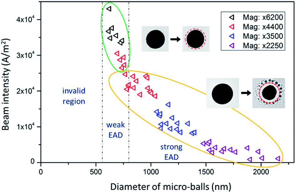 | ||
| Fig. 2 The influences of beam intensity and micro-ball size on the validity of the EAD method. The region is divided into three parts, that is, invalid region, weak EAD region, and strong EAD region. The inset TEM images show the differences between weak EAD (up) and strong EAD (down) regions. The inset box shows the used TEM magnifications during EAD process and imaging. | ||
Benefiting from this in situ EAD method, the nanoparticles obtained possess ultraclean surfaces, and thereby provide an ideal case to reveal their intrinsic properties during growth. Fig. 3a shows a dark field image of an as-fabricated nanoparticle assembly formed around a Bi49Pb18Sn12In21 micro-ball on a thin carbon film. This fascinating nanoparticle assembly presents the pristine states of the gas-phase fabricated nanoparticles without any surface oxidation, passivation or contamination. A distinct feature is noted that the newly formed nanoparticles have a wide particle size distribution. To quantitatively estimate the size distribution, concentric circles are drawn from the micro-ball centre to divide the area into several rings. The nanoparticles located in each ring marked from area-A to area-I are statistically measured and plotted in Fig. 3b. As can be seen, the areas nearby the micro-ball contain well-grown nanoparticles with large mean particle size but scattered size distribution. The far-end areas contain mostly homogeneous small nanoparticles with a mean size of around 6 nm. The large nanoparticles in areas A and B are sparse in comparison with those in the far-end areas, indicating that Ostwald ripening and nanoparticle coalescences should have occurred severely during the growth process in these areas. Actually, these two factors are the most important determinants which govern the eventual morphology of the nanoparticle assembly. However, no direct observation has been achieved up to now, and the growth kinetics is generally inferred and understood by postmortem analyses.
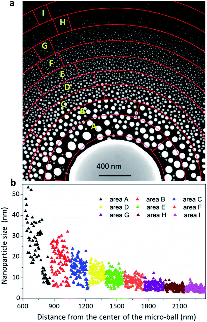 | ||
| Fig. 3 (a) Dark-field image of the as-fabricated alloy nanoparticles with an obvious size gradient. (b) Statically calculated nanoparticle size distribution by measuring the nanoparticle diameters in the marked areas from A to I in (a). The size distribution shows a rather scattered shape at the initial (area A), and gradually a convergent slope (areas G–I), implying that large nanoparticles should result from uneven coalescences. | ||
To visualize the dynamic process of nanoparticle growth, a large Bi49Pb18Sn12In21 micro-ball with diameter of around 2.4 μm is selected to enable EAD process under a moderate beam condition so that direct observation of the formation and growth processes of nanoparticles can be achieved synchronously in the same view (because the dose that a TEM camera can sustain is restricted). Fig. 4a shows a video frame of the dynamic process during nanoparticle growth (see ESI video for details†). The nanoparticles after nucleation are initially very small, similar to those fabricated by cluster beam deposition.16,33 The sites where the nanoparticles are pinned are possibly the defects in the carbon film. As a result, the number density of the nanoparticles could be saturated quickly, with regard to the surface conditions of the used supporting substrate. When all the defect sites are occupied, further EAD rarely leads to new nuclei in the carbon film. Thereby, the nanoparticles continuously grow up by direct atom deposition, diffusion, Ostwald ripening, and coalescences. In comparison with the first two approaches by which isolated nanoparticles grow independently, the Ostwald ripening and coalescence lead to uneven growth of some nanoparticles at the expense of others. Fig. 4b–j show the growth process and coalescence events occurred in the red box marked in Fig. 4a extracted from the selected video frames. Each colour tracks a sequence of coalescence events from the first merging of a group of nanoparticles. The dotted rings indicate the nanoparticles which will participate in the next coalescence. Strikingly, the coalescences are much more energetic than what they have been thought to be. In a coalescence event, a certain group of nanoparticles merges into each other in a flash, resulting in a single large one. Such events are discrepant from the conventional understandings that coalescences go through diffusion-driven inter-particle contacting, necking, and finally merging.34–37 This discrepancy provides direct evidence that free surfaces play a critical role in determining nanoparticle properties and behaviours. Although all the coalescences happen between neighbouring nanoparticles, the inter-particle spacing seems not to be the only criterion for judging the occurrence of such events. As shown in Fig. 4d and e, the nanoparticles indicated by dark yellow and purple are divided into two groups, and their eventual coalescences somehow break the criterion of inter-particle spacing. Similar cases are frequently observed and more details can be found in the ESI.† Judging from the dynamic evolutions, the electrostatic force is hypothesized to produce a certain influence. It may interpret the collective collision of a few nanoparticles in a single coalescence event, which is quite different from the conventional touching, necking and merging routine. By statistically analysing all the coalescence events in the video, the numbers of nanoparticles involved in each coalescence are shown in Fig. 4k. As can be seen, a large number of coalescence events involve two nanoparticles. However, a few coalescences are beyond nanoparticle pairs. In certain cases, as many as 6 nanoparticles can be involved in a single coalescence, demonstrating again the high activity of their pristine states.
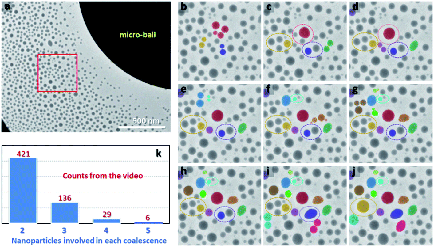 | ||
| Fig. 4 (a) A video frame captured from the dynamic growth process during EAD (see ESI video†). (b–j) The dynamic evolution of the nanoparticles in the region marked by the red box in (a). Each colour indicates the whole growth kinetics of a monitored nanoparticle group. The dashed circles indicate the occurred coalescences during further growth. (k) Statically calculated coalescence events involved 2, 3, 4, and 5 nanoparticles, respectively, from the video. | ||
The importance of free surfaces is further evidenced by verifying the oxidation of the EAD-fabricated nanoparticles. Fig. 5a shows a high-resolution TEM image of an EAD-fabricated nanoparticle after exposure to air for 5 hours. Obviously, a thin oxidation shell is formed with a thickness of around 1.1 nm. In this situation, the nanoparticles are well passivated, and even for the nanoparticle pairs which have already touched each other, coalescence can no longer occur during normal imaging (see ESI for details†). This comparison vividly uncovers that the surface effect definitely determines the growth of gas-phase nanoparticles during their coalescence stage, which is in sharp contrast to those slow diffusion-and-merging processes by postmortem observations.38,39 Noticeably, the EAD-fabricated nanoparticles from the Bi49Pb18Sn12In21 micro-ball offer an ideal model for exploring the phase diagram of nanoalloys. The nanoparticle in Fig. 5a exhibits a clear sandwich-like structure with outer parts identified as Pb and the inner part as Bi, differing from those alloyed nanostructures observed by Jesser et al.40 This nanoscale phase segregation implies a nearly stable structure according to the Pb–Bi binary phase diagram,40–42 providing an ideal case for verifying the structural and property deviation induced by size effect. Dark-field TEM characterization shows that phase segregation is an innate feature of the EAD-fabricated nanoparticles. As shown in Fig. 5b, distinct Z-contrast can be observed in the as-fabricated nanoparticles, representing sandwich-like or Janus-like patterns. By measuring the energy-dispersive spectra of the regions with different contrasts, as shown in Fig. 5c, Bi and Pb elements are easily identified by their fingerprints, in good agreement with the results obtained by measuring the lattice spacings. Noticeably, although there are four elements in the mother micro-balls, energy dispersive spectra of the EAD-fabricated nanoparticles only present Bi and Pb elements. This result is probably due to the discrepancy of saturation vapour pressures between these four elements. In other words, Bi and Pb have saturation vapour pressures several orders higher than Sn and In (see details in the ESI†).43 Thereby, evaporation/sublimation of Sn and In is extremely weak under this beam condition. This in return corroborates the conclusion that the EAD phenomenon is the result of local heat accumulation rather than electron sputtering.
 | ||
| Fig. 5 (a) High-resolution TEM image of a sandwich-type PbBi alloy nanoparticle after exposure to the atmosphere. The two outer parts correspond to Pb while the inner part marked in yellow corresponds to Bi. (b) Dark-field image of the as-fabricated PbBi alloy nanoparticles obtained by the EAD method. The nanoparticles show clear phase segregations with sandwich-type and Janus-type. (c) Energy dispersive spectra acquired from the two points marked in (b). The spectra suggest that the brighter part of the PbBi nanoparticle in (b) indicates a Bi-dominated phase and that the darker parts indicate Pb-dominated phases. (d and e) Identification of nanometre-sized surface steps in the substrate from the size distributions of the EAD nanoparticles. The yellow dashed lines indicate the boundary of the surface steps. The insets show the schematic illustration of the identified surface steps. | ||
Aside from the novel structures and properties, it is interesting to find that the EAD nanoparticles are quite sensitive to the surface conditions of the substrates. During nanoparticle growth, the surface fluctuations and steps obviously cause inhomogeneity of mass distribution. A direct outcome is that the shadow regions receive less mass than other similar regions nearby the contour line, causing nanoparticles with abrupt size distributions. This feature enables the effective identification of surface steps of thin films beyond the contrast limit of TEM observations. Fig. 5d and e show the EAD nanoparticles dispersed on two different thin carbon films. Despite the common characteristic of a radiate size gradient, clear nanoparticle chains with abruptly increased sizes are observed on the supporting films, as indicated by the dashed yellow lines. These nanoparticle chains depict the domain boundaries and profile the surface relief or steps of the supporting carbon films. As illustrated by the insets in Fig. 5d and e, atomic surface steps lead to nuclei pinned at the boundary edges, which later block surface atom diffusion to some extent and cause an overgrowth of these nuclei. By comparing the size distributions of the EAD nanoparticles in the two domains around the boundary line, it is found that atomic height-drops lead to a decrease of mean nanoparticle size in the far-end domain from the mother micro-ball. In contrast, a surface step-up will not cause a significant decrease of mean nanoparticle size in the far-end domain, though the shadow effect of the nanoparticle chain at the boundary may cause a confined narrow region nearby comprising very small nanoparticles. In this principle, the surface steps which are usually transparent and invisible during normal TEM imaging can be easily distinguished and identified as step-down (Fig. 5d) and step-up (Fig. 5e), respectively. This method may be useful for characterizing the surface domain or roughness of two-dimensional thin materials as the EAD nanoparticles are easily sublimated at moderate temperatures and hence will not induce potential surface contaminations.
Experimental
Preparation of Bi49Pb18Sn12In21 micro-balls
The Bi49Pb18Sn12In21 bulk alloy was bought from a commercial company (MAT-CN, China). For a typical synthesis of micro-balls, a fragment of Bi49Pb18Sn12In21 was peeled off and placed into deionized water inside a beaker. The beaker was then put on a heating stage and heated up to 80–90 °C. When the deionized water reaches this target temperature, the beaker was quickly transferred to an ultrasonic oscillator and vibrated for 60 seconds. During this process, the molten Bi49Pb18Sn12In21 was drastically vibrated and the clean deionized water turned into the turbid solution due to the formation of Bi49Pb18Sn12In21 micro-balls. Later, a portion of the turbid solution was absorbed using a glass pipette and then dispersed onto the selected substrates after it cools down to room temperature.TEM characterization and recording
An aberration-corrected high-resolution TEM (FEI Titan 80-300) was used to perform characterizations with an accelerating voltage of 300 kV. During normal imaging, the beam intensity was used in a range of 103–105 A m−2. In order to examine the condition of EAD occurrence, the e-beam was first spread out widely to have quite a low beam intensity during sample searching. When the micro-balls were selected, the e-beam was converged on the micro-balls step by step. Meanwhile, the corresponding beam intensity and magnifications were recorded synchronously. For dynamic video recording, the beam intensity was set to be lower than the normal TEM imaging to slow down the EAD process. The preview mode was used with an exposure time of 0.2 S. So the video was recorded at a rate of around 3 frames per second. The energy-dispersive spectra were acquired using scanning-TEM mode. The Z-contrast dark-field image was also acquired in this mode with a high angle annular detector.Conclusions
In summary, a novel EAD method is developed to in situ fabricate ultra-clean gas-phase alloy nanoparticles. This EAD method facilitates the direct visualization of the growth kinetics and dynamic evolutions of gas-phase fabricated alloy nanoparticles. It is found that e-beam induced local heating on micro-balls is the critical point determining the feasibility of this EAD method. The local heat accumulation inside the mother micro-ball enables efficient evaporation/sublimation, while the surrounding areas with normal temperature make nanoparticle nucleation and growth achievable. The nucleation, growth kinetics and coalescence dynamics of the EAD-fabricated nanoparticles, as well as their size distributions, are visualized and analysed. It is found that the EAD-fabricated nanoparticles with ultra-clean surfaces are extremely energetic in their pristine states. Nanoparticle growth and coalescence take place in a manner beyond conventional understandings by postmortem characterizations. Moreover, the EAD-fabricated BiPb nanoparticles present sandwich-like or Janus-like phase-segregated heterostructures. These novel alloy or phase-segregated structures can provide an ideal model for exploring the deviation of the nanoscale binary phase diagram in comparison to their bulk counterparts. Finally, the size distributions of the EAD nanoparticles are found to be very sensitive to surface defects and surface relief. This EAD method and resulting nanoparticles can be used to identify the atomic surface steps and domains in thin films which are usually transparent and invisible in normal TEM characterizations.Conflicts of interest
There are no conflicts to declare.Acknowledgements
This work is supported by the National Key R&D Program of China Grant No. 2017YFA0305500, the National Natural Science Foundation of China (Grant No. 51571060 and 11774050), and the Aero-Science Fund ASFC-20170269003.References
- M. Benelmekki, An introduction to nanoparticles and nanotechnology, in: Designing Hybrid Nanoparticles, Morgan & Claypool Publishers, 2015 Search PubMed.
- M. C. Daniel and D. Astruc, Chem. Rev., 2004, 104, 293–346 CrossRef CAS PubMed.
- C. J. Murphy, T. K. San, A. M. Gole, C. J. Orendorff, J. X. Gao, L. Gou, S. E. Hunyadi and T. Li, J. Phys. Chem. B, 2005, 109, 13857–13870 CrossRef CAS PubMed.
- Y. G. Sun and Y. N. Xia, Science, 2002, 298, 2176–2179 CrossRef CAS PubMed.
- S. Berciaud, L. Cognet, P. Tamarat and B. Lounis, Nano Lett., 2005, 5, 515–518 CrossRef CAS PubMed.
- L.-B. He, L. Zhang, L.-P. Tang, J. Sun, Q.-B. Zhang and L.-T. Sun, Mater. Today Nano, 2018, 1, 8–21 CrossRef.
- Y. Volokitin, J. Sinzig, L. J. deJongh, G. Schmid, M. N. Vargaftik and I. I. Moiseev, Nature, 1996, 384, 621–623 CrossRef CAS.
- L. He, X. Chen, Y. Mu, F. Song and M. Han, Nanotechnology, 2010, 21, 495601 CrossRef PubMed.
- Q. Li, X. Zhuo, S. Li, Q. Ruan, Q.-H. Xu and J. Wang, Adv. Opt. Mater., 2015, 3, 801–812 CrossRef CAS.
- D. R. Lu, J. J. Zhou, S. Hou, Q. R. Xiong, Y. H. Chen, K. Y. Pu, J. H. Ren and H. W. Duan, Adv. Mater., 2019, 31, 1902733 CrossRef CAS PubMed.
- J. Park, K. J. An, Y. S. Hwang, J. G. Park, H. J. Noh, J. Y. Kim, J. H. Park, N. M. Hwang and T. Hyeon, Nat. Mater., 2004, 3, 891–895 CrossRef CAS PubMed.
- X. G. Peng, L. Manna, W. D. Yang, J. Wickham, E. Scher, A. Kadavanich and A. P. Alivisatos, Nature, 2000, 404, 59–61 CrossRef CAS PubMed.
- S. H. Sun, C. B. Murray, D. Weller, L. Folks and A. Moser, Science, 2000, 287, 1989–1992 CrossRef CAS PubMed.
- Y. Xia, Y. Xiong, B. Lim and S. E. Skrabalak, Angew. Chem., Int. Ed., 2009, 48, 60–103 CrossRef CAS PubMed.
- J. C. Yu, T. W. Zhang, H. T. Xu, X. L. Dong, Y. Cai, Y. X. Pan and C. Q. Cao, RSC Adv., 2019, 9, 39381–39393 RSC.
- M. Han, C. Xu, D. Zhu, L. Yang, J. Zhang, Y. Chen, K. Ding, F. Song and G. Wang, Adv. Mater., 2007, 19, 2979–2983 CrossRef CAS.
- L. B. He, Y. L. Wang, X. Xie, M. Han, F. Q. Song, B. J. Wang, W. L. Chen, H. X. Xu and L. T. Sun, Phys. Chem. Chem. Phys., 2017, 19, 5091–5101 RSC.
- G. Benetti, E. Cavaliere, R. Brescia, S. Salassi, R. Ferrando, A. Vantomme, L. Pallecchi, S. Pollini, S. Boncompagni, B. Fortuni, M. J. Van Bael, F. Banfi and L. Gavioli, Nanoscale, 2019, 11, 1626–1635 RSC.
- Y. Gong, Y. Zhou, L. He, B. Xie, F. Song, M. Han and G. Wang, Eur. Phys. J. D, 2013, 67, 87 CrossRef.
- J. G. Mattei, P. Grammatikopoulos, J. L. Zhao, V. Singh, J. Vernieres, S. Steinhauer, A. Porkoyich, E. Danielson, K. Nordlund, F. Djurabekova and M. Sowwan, Chem. Mater., 2019, 31, 2151–2163 CrossRef CAS.
- P. Solar, O. Polonskyi, A. Olbricht, A. Hinz, A. Shelemin, O. Kylian, A. Choukourov, F. Faupel and H. Biederman, Sci. Rep., 2017, 7, 8514 CrossRef PubMed.
- P. Mao, C. Liu, G. Favraud, Q. Chen, M. Han, A. Fratalocchi and S. Zhang, Nat. Commun., 2018, 9, 5428 CrossRef CAS PubMed.
- M. R. Hauwiller, L. B. Frechette, M. R. Jones, J. C. Ondry, G. M. Rotskoff, P. Geissler and A. P. Alivisatos, Nano Lett., 2018, 18, 5731–5737 CrossRef CAS PubMed.
- M. R. Hauwiller, X. W. Zhang, W. I. Liang, C. H. Chiu, Q. Zhang, W. J. Zheng, C. Ophus, E. M. Chan, C. Czarnik, M. Pan, F. M. Ross, W. W. Wu, Y. H. Chu, M. Asta, P. W. Voorhees, A. P. Alivisatos and H. M. Zheng, Nano Lett., 2018, 18, 6427–6433 CrossRef CAS PubMed.
- B. H. Kim, J. Yang, D. Lee, B. K. Choi, T. Hyeon and J. Park, Adv. Mater., 2018, 30, 1703316 CrossRef PubMed.
- H. G. Liao, L. K. Cui, S. Whitelam and H. M. Zheng, Science, 2012, 336, 1011–1014 CrossRef CAS PubMed.
- H. M. Zheng, R. K. Smith, Y. W. Jun, C. Kisielowski, U. Dahmen and A. P. Alivisatos, Science, 2009, 324, 1309–1312 CrossRef CAS PubMed.
- C. Zhu, S. X. Liang, E. H. Song, Y. J. Zhou, W. Wang, F. Shan, Y. T. Shi, C. Hao, K. B. Yin, T. Zhang, J. J. Liu, H. M. Zheng and L. T. Sun, Nat. Commun., 2018, 9, 421 CrossRef PubMed.
- Y. Chen, Y. L. Huang, N. S. Liu, J. Su, L. Y. Li and Y. H. Gao, Sci. Rep., 2015, 5, 11313 CrossRef CAS PubMed.
- J. Gong, S. Yang, H. Huang, X. Zhao and Z.-Z. Yu, Nanotechnology, 2007, 18, 235606 CrossRef.
- J. M. Voss, P. K. Olshin, R. Charbonnier, M. Drabbels and U. J. Lorenz, ACS Nano, 2019, 13, 12445–12451 CrossRef CAS PubMed.
- X. L. Wei, D. M. Tang, Q. Chen, Y. Bando and D. Golberg, ACS Nano, 2013, 7, 3491–3497 CrossRef CAS PubMed.
- M. Han, Z. Y. Wang, P. P. Chen, S. W. Yu and G. H. Wang, Nucl. Instrum. Methods Phys. Res. Sect. B Beam Interact. Mater. Atoms, 1998, 135, 564–569 CrossRef CAS.
- M. A. Asoro, D. Kovar, Y. Shao-Horn, L. F. Allard and P. J. Ferreira, Nanotechnology, 2010, 21, 025701 CrossRef CAS PubMed.
- Y. Jiang, Y. Wang, Y. Y. Zhang, Z. F. Zhang, W. T. Yuan, C. H. Sun, X. Wei, C. N. Brodsky, C. K. Tsung, J. X. Li, X. F. Zhang, S. X. Mao, S. B. Zhang and Z. Zhang, Nano Res., 2014, 7, 308–314 CrossRef CAS.
- D. S. Li, M. H. Nielsen, J. R. I. Lee, C. Frandsen, J. F. Banfield and J. J. De Yoreo, Science, 2012, 336, 1014–1018 CrossRef CAS PubMed.
- E. Longo, W. Avansi, J. Bettini, J. Andres and L. Gracia, Sci. Rep., 2016, 6, 21498 CrossRef CAS PubMed.
- S. H. Cha, Y. Park, J. W. Han, K. Kim, H. S. Kim, H. L. Jang and S. Cho, Sci. Rep., 2016, 6, 32951 CrossRef CAS PubMed.
- M. Grouchko, P. Roitman, X. Zhu, I. Popov, A. Kamyshny, H. B. Su and S. Magdassi, Nat. Commun., 2014, 5, 2994 CrossRef PubMed.
- W. A. Jesser, R. Z. Shneck and W. W. Gile, Phys. Rev. B, 2004, 69, 144121 CrossRef.
- Y. Magnin, A. Zappelli, H. Amara, F. Ducastelle and C. Bichara, Phys. Rev. Lett., 2015, 115, 205502 CrossRef CAS PubMed.
- F. Q. Zu, Z. G. Zhu, B. Zhang, Y. Feng and J. P. Shui, J. Phys.: Condens. Matter, 2001, 13, 11435–11442 CrossRef CAS.
- C. L. Yaws, Handbook of vapor pressure: volume 4: inorganic compounds and elements, Gulf Professional Publishing, 1995 Search PubMed.
- J. Ju and W. Chen, Anal. Chem., 2015, 87, 1903–1910 CrossRef CAS PubMed.
- D. L. Huber, Small, 2005, 1, 482–501 CrossRef CAS PubMed.
- T. Terao, Y. Bando, M. Mitome, C. Zhi, C. Tang and D. Golberg, J. Phys. Chem. C, 2009, 113, 13605–13609 CrossRef CAS.
- A. J. Bullen, K. E. O'Hara, D. G. Cahill, O. Monteiro and A. van Keudell, J. Appl. Phys., 2000, 88, 6317–6320 CrossRef CAS.
- X. Zhang and C. P. Grigoropoulos, Rev. Sci. Instrum., 1995, 66, 1115–1120 CrossRef CAS.
Footnotes |
| † Electronic supplementary information (ESI) available. See DOI: 10.1039/d0ra01740j |
| ‡ These authors contributed equally to this work. |
| This journal is © The Royal Society of Chemistry 2020 |