
 Open Access Article
 This Open Access Article is licensed under a
 Creative Commons Attribution 3.0 Unported Licence
The growth of methylammonium lead iodide perovskites by close space vapor transport
Alexander J. Harding ab,
Austin G. Kubaab,
Brian E. McCandlessa,
Ujjwal K. Dasa,
Kevin D. Dobsona,
Babatunde A. Ogunnaikec and
William N. Shafarman*ab
ab,
Austin G. Kubaab,
Brian E. McCandlessa,
Ujjwal K. Dasa,
Kevin D. Dobsona,
Babatunde A. Ogunnaikec and
William N. Shafarman*ab
aInstitute of Energy Conversion, University of Delaware, Newark, Delaware 19716, USA. E-mail: wns@udel.edu; Tel: +1-302-831-6200
bMaterials Science and Engineering, University of Delaware, Newark, DE 19716, USA
cChemical and Biomolecular Engineering, University of Delaware, Newark, DE 19716, USA
First published on 23rd April 2020
Abstract
Vapor deposition processes have shown promise for high-quality perovskite solar cells with potential pathways for scale-up to large area manufacturing. Here, we present a sequential close space vapor transport process to deposit CH3NH3PbI3 (MAPI) perovskite thin films by depositing a layer of PbI2 then reacting it with CH3NH3I (MAI) vapor. We find that, at T = 100 °C and pressure = 9 torr, a ∼225 nm-thick PbI2 film requires ≥125 minutes in MAI vapor to form a fully-reacted MAPI film. Raising the temperature to 160 °C increases the rate of reaction, such that MAPI forms within 15 minutes, but with reduced surface coverage. The reaction kinetics can be approximated as roughly first-order with respect to PbI2, though there is evidence for a more complicated functional relation. Perovskite films reacted at 100 °C for 150 minutes were fabricated into solar cells with an SLG/ITO/CdS/MAPI/Spiro-OMeTAD/Au structure, and a device efficiency of 12.1% was achieved. These results validate the close space vapor transport process and serve as an advance toward scaled-up, vapor-phase perovskite manufacturing through continuous vapor transport deposition.
1 Introduction
As the stability1,2 and efficiency3–6 of lead halide perovskite solar cells improve, scaling laboratory performance to industrial production becomes increasingly important. The majority of published research currently focuses on scaling established perovskite spin-coating processes to continuous solution processes such as slot-die coating or blade-coating.7–11 However, high-efficiency perovskites can be fabricated using a variety of vapor deposition techniques with established pathways to solvent-free, scaled-up manufacturing.12–15 One such method is “close space vapor transport” (CSVT), which serves as a laboratory precursor for large-area, commercial production through vapor transport deposition (VTD).16 In CSVT, the source material of interest is evaporated into a carrier gas, transported to a substrate, and condensed to form a thin film. The technique provides insight into how different temperature and pressure regimes, in various carrier-gas environments, can be used to control the deposition rate, uniformity, and crystallinity of the deposited films before designing and implementing scaled-up VTD reactors. CSVT has been used extensively for CdTe solar cell research, where it was regularly used to produce high-quality films that resulted in high-efficiency solar cells.16 This fostered the deployment of a commercial VTD process for large-area, uniform CdTe deposition by First Solar LLC.16Despite this success, an all-vapor CSVT process for perovskite thin film deposition has not been investigated. Therefore, feasible processing temperatures and pressures have not been defined, and their effect on deposition rate, film quality, and device performance are unknown. There are only a few reports of methylammonium iodide (CH3NH3I, MAI) reactions in a CSVT configuration with spin-coated PbI2 followed by annealing to drive a reaction between PbI2 and MAI vapor.17–19 However, these studies do not provide sufficient information to develop a VTD reactor for scaled-up perovskite manufacturing because they omit the vapor deposition of the PbI2 film.
The application of an all-vapor CSVT process to directly deposit methylammonium lead iodide (CH3NH3PbI3, MAPI) thin films must differ from CdTe deposition by CSVT, where the absorber sublimes from a single molecular source to form Cd and Te2 vapors that react at the substrate and form a solid film,16 because the vapor pressures of the constituent compounds of MAPI perovskites (PbI2 and MAI) are too dissimilar to deposit stoichiometric films from a single source.20,21 Therefore, a two-stage CSVT process has been developed to form the MAPI absorber layer by depositing a film of PbI2 and reacting it in MAI vapor as shown in Fig. 1. Here we report the deposition of PbI2 films via CSVT, their reaction with MAI vapor, a reaction kinetic model, an upper-threshold to reaction temperature, and functional devices achieving 12.1% efficiency.
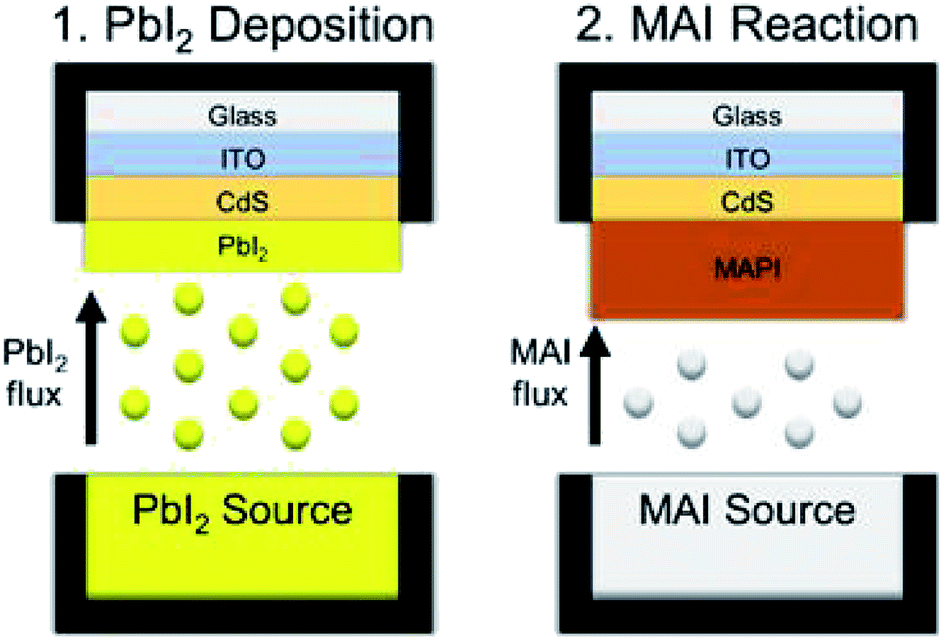 | ||
| Fig. 1 A schematic of the two-stage CSVT process used to deposit MAPI thin films. | ||
2 Experimental approach
2.1 Substrate preparation
Soda-lime glass (SLG) substrates were sequentially cleaned by sonication in LiquiNOX® and CitraNOX® soaps, followed by rinsing in DI water and drying at 180 °F for 1 hour. After drying, a 300 nm layer of ITO was RF sputtered at room temperature onto the substrates through a shadow mask to define cell area.2.2 CdS deposition by chemical surface deposition
CdS was chosen as the electron transport layer because its conduction band lies 0.3 eV below the perovskite's conduction band and due to its good hole-blocking properties.22 CdS was deposited on the ITO-coated SLG substrates using chemical surface deposition (CSD).23 The SLG/ITO substrates were heated on a hot plate to 55 °C and a solution was prepared containing 2.2 mL 1.5 mM CdSO4 (99.996%, Alfa Aesar), 2.2 mL 1.5 M thiourea (99%, Alfa Aesar), 2.8 mL 30% NH4OH (JT Baker) and 15 mL DI water. Afterward, 1.5 mL of the solution was dispensed dropwise onto each of the hot substrates. After 5 minutes, the substrates were removed from heat, tipped of fluid, rinsed with flowing DI water, and dried with argon. The process was repeated to apply a second coat of CdS, yielding a uniform, ≈50 nm thick layer.2.3 CSVT reactor
A photograph of the CSVT reactor developed for these experiments is shown in Fig. 2a. It consists of a planar source-substrate geometry with the source positioned beneath the substrate. A motorized arm is used to position the apparatus in a 4.5 cm diameter quartz tube between two 1000 W lamps. These lamps independently heat two graphite susceptors, which are in direct contact with the source material and the substrates, as seen in Fig. 2b. Eurotherm 2404 controllers moderate the temperature of each susceptor using embedded thermocouples so that the heating lamps control the source and substrate temperatures between 25 and 500 °C. A roughing pump, an argon carrier gas flowing at 10 sccm, two Baratron capacitance manometers, and a throttle valve maintain the working pressure between 0.1 and 100 torr. The CSVT reactor is integrated with a multi-function glove box used to prepare, load, and unload the sources and substrates in a nitrogen atmosphere with O2 < 0.1 ppm and H2O < 5 ppm. This allows the perovskite layer to be processed start-to-finish without exposure to ambient air.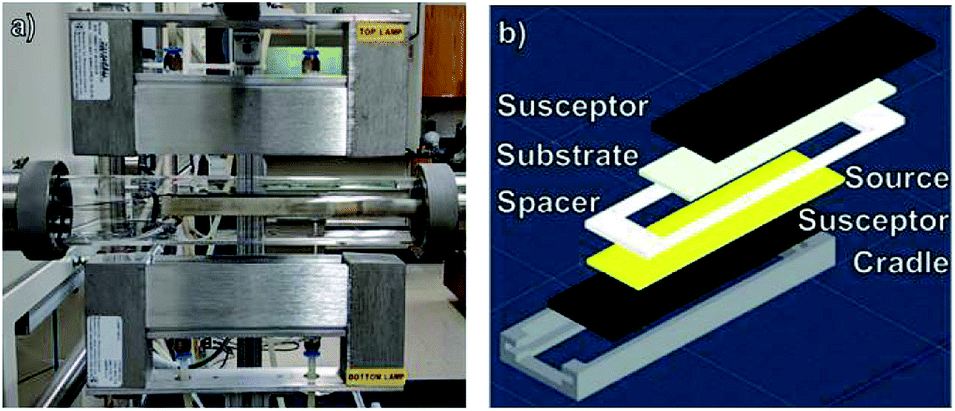 | ||
| Fig. 2 (a) A photograph of the CSVT reactor. (b) An exploded view of the CSVT fixture and its components. | ||
Fig. 2b shows an exploded schematic of the source and substrate holder. Insulating Macor® ceramic fittings hold the 10.8 cm long source and substrate susceptors in place and maintain a temperature gradient across a 2.2 mm gap defined by the spacer. This gradient promotes mass transport from the source to the substrates, resulting in deposition and film growth. The fittings also define the deposition area to be ≈20 cm2, which accommodates three 2.5 cm × 2.5 cm substrates per run.
CSVT processing of MAPI is shown schematically in Fig. 1. CdS-coated SLG/ITO substrates are loaded face down into the CSVT chamber over a PbI2 source, and the system is pumped to a base pressure of 10−7 torr. The chamber is then backfilled with argon gas to a fixed working pressure, and the system is allowed to equilibrate for 5 min. The lamps ramp the source and substrate susceptors to their temperature setpoints over 5 min at a fixed rate of 47 °C min−1 for the source and 38 °C min−1 for the substrate. The source and substrate temperatures are then controlled to within ±2 °C of their setpoints for a specified duration by independently modulating the top and bottom lamp power.
Following PbI2 deposition, the PbI2-coated substrates and the PbI2 source are unloaded from the CSVT reactor. Then a second source, filled with MAI powder, is loaded into the CSVT reactor with the PbI2-coated substrates. After pumping and backfilling, the source and the substrate susceptors are heated to their setpoints at a rate of 25 °C min−1. MAI sublimes and saturates the headspace surrounding the PbI2 film, driving a solid–vapor reaction to form MAPI. Finished MAPI films are removed from the CSVT chamber into the glove box, washed with isopropanol (anhydrous 99.5%, Sigma Aldrich) to remove residual MAI, blow-dried with argon, and annealed on a hot-plate at 100 °C for 5 minutes.
2.4 Rear contact preparation
Spiro-OMeTAD (Spiro) (99%, Sigma Aldrich) films were deposited using an established recipe from literature.24 The Spiro solution was stirred for 10 minutes and filtered through a 0.2 μm PTFE filter to remove large particles prior to spin-coating. Spiro films were dynamically spin-coated by aliquoting 100 μL of solution onto the substrate at 4000 rpm for 10 seconds. The films were dried and stored in the dark in a dry air desiccator (relative humidity < 7.5%) overnight prior to metallization.Oxidized SLG/ITO/CdS/MAPI/Spiro samples were loaded into an electron beam evaporator and pumped to a base pressure of 10−6 torr. Gold films were deposited through a shadow mask at a rate of 6 Å s−1 to a final thickness of 100 nm. The active area of the solar cells was defined by the overlap area between the gold and the ITO to be 0.24 cm2. The edges of the perovskite were removed with a razor blade to expose the ITO contacts, and silver paste was applied using Dotite® D-550 Silver Colloid (2SPI).
2.5 Device measurement
Current–voltage (J–V) measurements were carried out using a setup maintained in the N2-filled glovebox. The intensity of a xenon arc lamp (Newport Oriel 67005 Housing; Newport Oriel 69907 Power Supply) was calibrated using a Si solar cell with a Schott KG-5 IR filter attached to the front. This limits the spectral sensitivity of the Si calibration cell to 800 nm and matches the spectral sensitivity of the calibration cell to test devices. The calibration value is based on quantum efficiency (QE) measurements and J–V measurements on a class A Oriel solar simulator.J–V measurements were carried out in a 4-point probe configuration with scans between −0.4 and 1.2 V at a sweep rate of 200 V s−1 with 48 data points. Cells were scanned from reverse to forward bias then back. Afterward, cells were pre-biased at 1.2 V for 60 seconds prior to measurement from 1.2 V forward bias to −0.4 V reverse bias. The data exhibited minor oscillations due to capacitive coupling between the device and the source measure unit (SMU) or temporal variations in the light intensity, and, therefore, the data was smoothed using a 5-point adjacent average for clarity.
2.6 Materials characterization
Three scanning electron microscopes (SEM) were used to collect micrographs of various samples. An AMRAY 1810T Digital SEM was used at an accelerating voltage of 20 kV to image MAPI samples reacted at 160 °C and perform energy dispersive X-ray spectroscopy (EDS). A Zeiss Auriga 60 High Resolution Field Emission SEM and a JSM-7400 High Resolution SEM were used at 3 kV to image plan-view and cross-section imaging, respectively.X-ray fluorescence (XRF) measurements were obtained using an Oxford Instruments X-Strata 980 Coating Thickness Analyser to measure the thickness of the PbI2 films. Samples were measured over a 0.75′′ × 0.875′′ area of the film using a 7 × 8 grid for a total of 56 equally-spaced data points that were used to determine the average thickness of each film.
The CSVT films were analyzed by X-ray diffraction (XRD) using a Philips/Norelco powder X-ray diffractometer using a CuKα X-ray source operating at 35 kV and 20 mA in Bragg–Brentano parafocusing geometry. The scan settings were 0.05° 2θ per step with a 4 second dwell time, over the 2θ range 10–30° to cover the principal peaks of PbI2 and MAPI. The XRD data was smoothed and processed with the Rachinger correction to remove contributions from CuKα2.25 All peaks were indexed and assigned to phases based on d-spacing conformity with references for ITO (cubic In2O3, ICDD 00-006-0416), PbI2 (hexagonal, ICDD 01-080-1000), and MAPI (tetragonal, pattern generated using PowderCell 2.0 for space group I4cm).
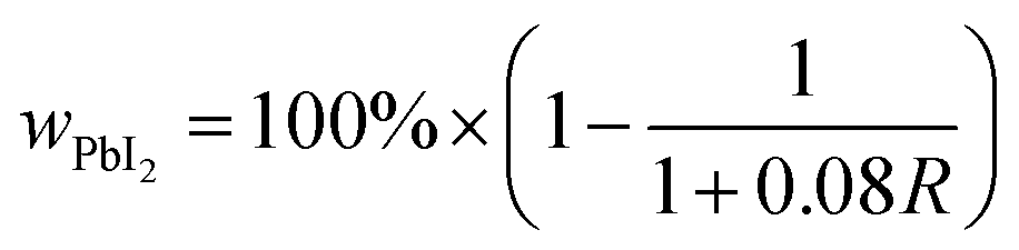
The weight percent of PbI2 (wPbI2) in each sample was estimated from the intensity ratio (R) of the PbI2 (001) and MAPI (110) reflections, corrected for background, using standard quantitative powder diffraction analysis as shown in eqn (1).26 The detection limit of ≈0.1% is governed by the signal-to-noise of the data, which is governed by the scattering power of each phase, the instrumental noise, and the scan conditions.
 | (1) |
3 Results
3.1 Deposition of PbI2 thin films
Previous research indicates that for single-junction, perovskite solar cells, the optimal thickness of the MAPI absorber layer is ≈400 nm,27 which requires the PbI2 precursor film to be ≈200 nm thick.28 PbI2 was deposited using a source temperature (Tsource) = 260 °C, and a substrate temperature (Tsub) = 215 °C, according to a Clausius–Clapeyron fit of its vapor pressure ,20 to produce a vapor pressure difference of two orders of magnitude between the source (Pvapsource) = 2 × 10⁻⁶ ± 8 × 10⁻⁷ torr and the substrate (Pvapsub) = 6 × 10⁻⁸ ± 3 × 10⁻⁸ torr. Depositions were carried out at a pressure (P) = 1 torr and the deposition time (t) was varied to achieve a desired film thickness. A 20 min deposition (t = 20 min) produced films with an average thickness of 225 ± 7 nm, measured by XRF.
The XRD pattern of a PbI2 film on an SLG/ITO/CdS substrate shown in Fig. 3a is fully indexed using hexagonal PbI2 and cubic In2O3 standards. Notably, CdS diffraction peaks are not observed due its low thickness (≈50 nm) and poor crystallinity. The PbI2 XRD pattern shows the strongest diffraction peak at 2θ = 12.60°, which corresponds to the (001) basal plane of hexagonal PbI2. In a random pattern of PbI2 powder, the brightest peak occurs at 25.90° and corresponds to the (011) plane. This suggests that the PbI2 films deposited on CdS orient around the basal plane during the deposition process.
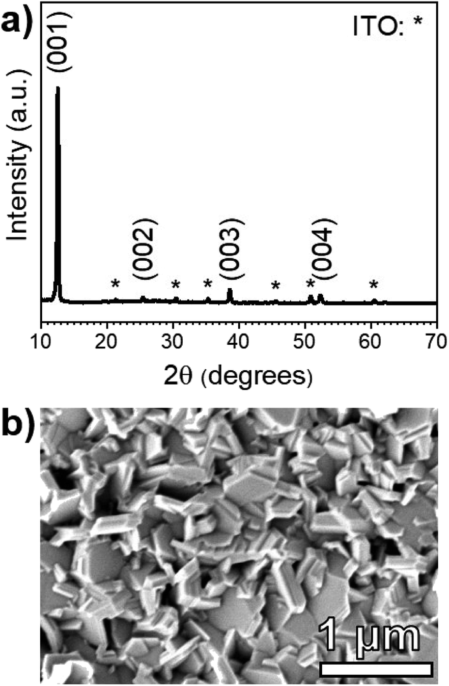 | ||
| Fig. 3 (a) XRD pattern of a ≈ 225 nm thick PbI2 film deposited on an SLG/ITO/CdS substrate at Tsource = 260 °C, Tsub = 215 °C, P = 1 torr, and t = 20 min. The principal PbI2 planes are labeled at their respective diffraction peaks, and the ITO peaks are marked with an asterisk. (b) A plan-view SEM micrograph of the PbI2 film. | ||
Fig. 3b shows a plan-view SEM micrograph of the same PbI2 film. The morphology consists of hexagonal platelets that are consistent with the quasi-two-dimensional, 2H polytype of the PbI2 hexagonal crystal structure.29 While the film appears to have a rough texture, the PbI2 platelets seem to fully coat the CdS substrate with no visible pinholes.
3.2 Reaction of PbI2 in MAI vapor
MAI reactions of PbI2 films were carried out isothermally at Tsource = Tsub = 100 °C. The amount of MAI participating in the reaction is estimated from a Clausius–Clapeyron fit of the vapor pressure,21 which gives PvapMAI = 50 ± 20 mTorr at T = 100 °C. The system pressure was maintained at a constant P = 9 torr using an argon ambient, which diluted the concentration of MAI vapor.A series of reactions were carried out from 25–150 min in 25 min increments. Fig. 4a shows the XRD patterns of the reacted films at each point in time. The conversion of PbI2 to MAPI is confirmed by the disappearance of the PbI2 (001) diffraction peak at 12.60° and the appearance of the MAPI (110) and (220) peaks at 14.05° and 28.40° respectively. The PbI2 (001) intensity decreases and the MAPI (110) signal increases with increasing reaction time. After a 125 min reaction, the PbI2 signal is indistinguishable from the background. The morphology of the 150 min-reacted film from Fig. 4a is shown in Fig. 4b. The film has a dense morphology that appears to be continuous across the CdS substrate without visible pinholes.
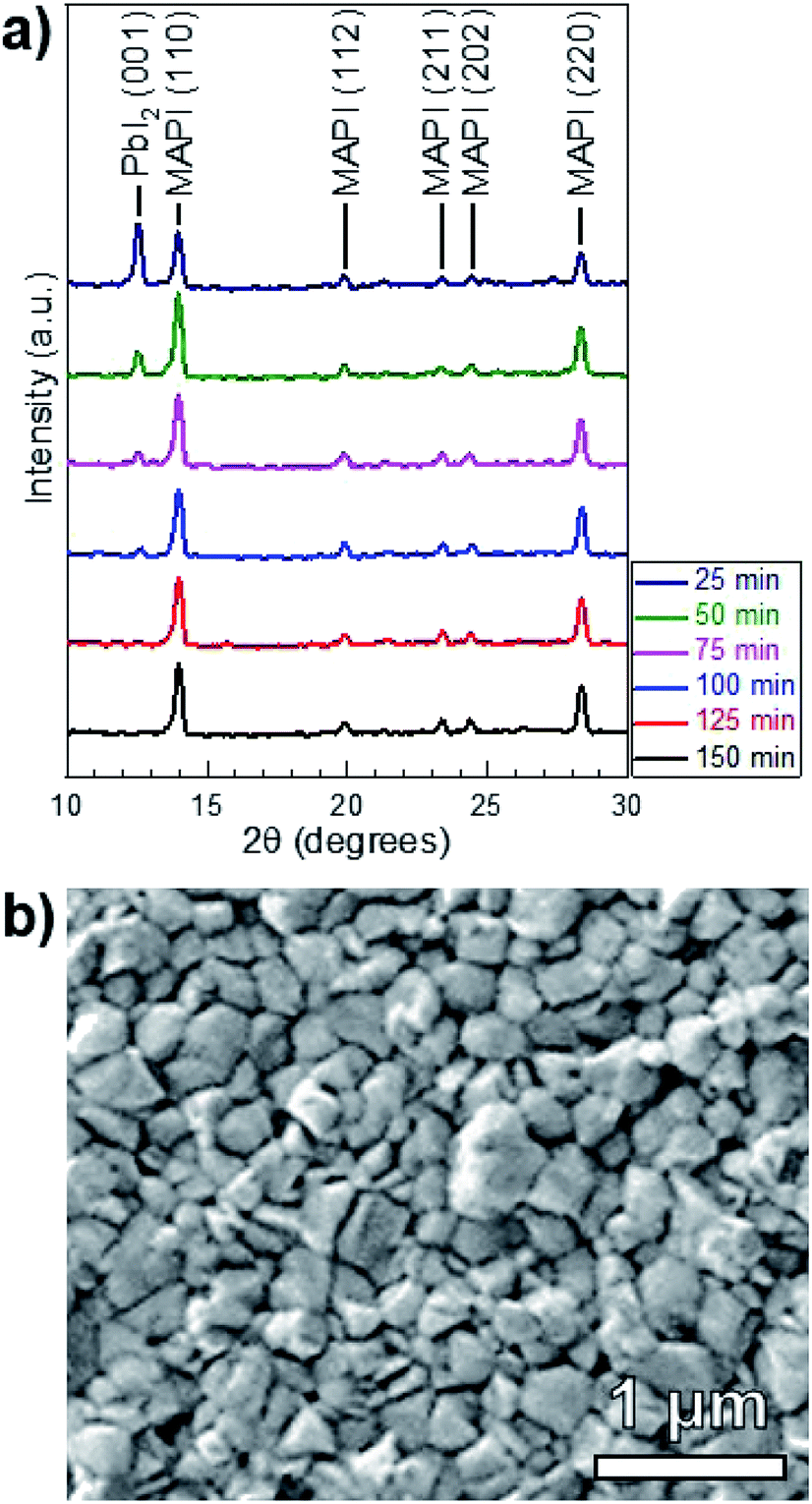 | ||
| Fig. 4 (a) XRD patterns of MAPI films reacted isothermally in MAI at T = 100 °C and P = 9 torr for durations t = 25–150 min. The principal PbI2 and tetragonal MAPI peaks (space group I4cm) are labeled. (b) A plan-view SEM micrograph of the MAPI film reacted for 150 min. | ||
Quantitative X-ray diffraction intensity analysis26 was performed on the XRD patterns shown in Fig. 4a. A comparison of the PbI2 (001) and MAPI (110) peak intensities yielded the weight percent of PbI2 as a function of the reaction time, which was converted to moles (NPbI2) and plotted in Fig. 5. As t increases, NPbI2 decreases as it is converted to MAPI. This shows >99% conversion from PbI2 to MAPI after t = 125 min at T = 100 °C and P = 9 torr.
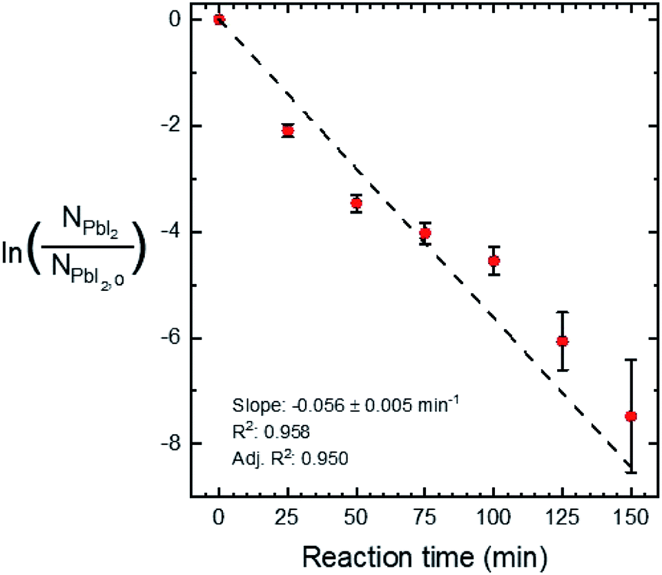 | ||
| Fig. 5 The natural log of NPbI2 normalized to NPbI2,o versus reaction time. The error bars show 95% confidence intervals with increasing uncertainty with increasing reaction time, due to a decreasing signal-to-noise ratio in the XRD measurement. A linear fit of the data is shown along with its slope, R2, and adjusted R2. | ||
A linear fit of the data in Fig. 5 is used to approximate the first-order kinetic expression in eqn (2), where k is the rate constant and t is reaction time.
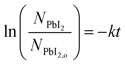 | (2) |
The associated R2-value of 0.958, and an adjusted-R2-value of 0.950, indicate that the first-order kinetic model is in reasonable agreement with the data; however, there is some visual evidence of curvature in the data, which may indicate a slightly more complicated functional relation. Consequently, we estimate the reaction rate constant, k, from the slope of the line as k = 0.056 ± 0.005 min−1. While this rate parameter is low, leading to reactions requiring 150 min to reach >99% completion, it is likely to be a function of the reaction temperature and the concentration of MAI vapor, which are not explicitly included in the first-order model of eqn (2). This suggests that the reaction temperature and pressure can be tuned for faster reactions.
To investigate the effect of increased temperature and MAI concentration, another set of MAI reactions were carried out at T = 160 °C and P = 9 torr, corresponding to an MAI vapor pressure of PvapMAI = 6 ± 1 torr21—approximately two orders of magnitude higher than that of the 100 °C reactions. Fig. 6a shows the XRD patterns of films after 10 and 15 min reactions. There is a distinct PbI2 (001) peak at 12.60° for the 10 min reaction, whereas the PbI2 peak is indistinguishable from the background after 15 min. According to our quantitative analysis, this indicates >99% conversion from PbI2 to MAPI. This reaction at T = 160 °C is an order of magnitude faster than the reaction at T = 100 °C—indicating the rate of reaction is, in fact, a function of temperature. It is worth noting that the MAPI (112), (211), and (202) peaks are present in both the 10 and 15 min reactions.
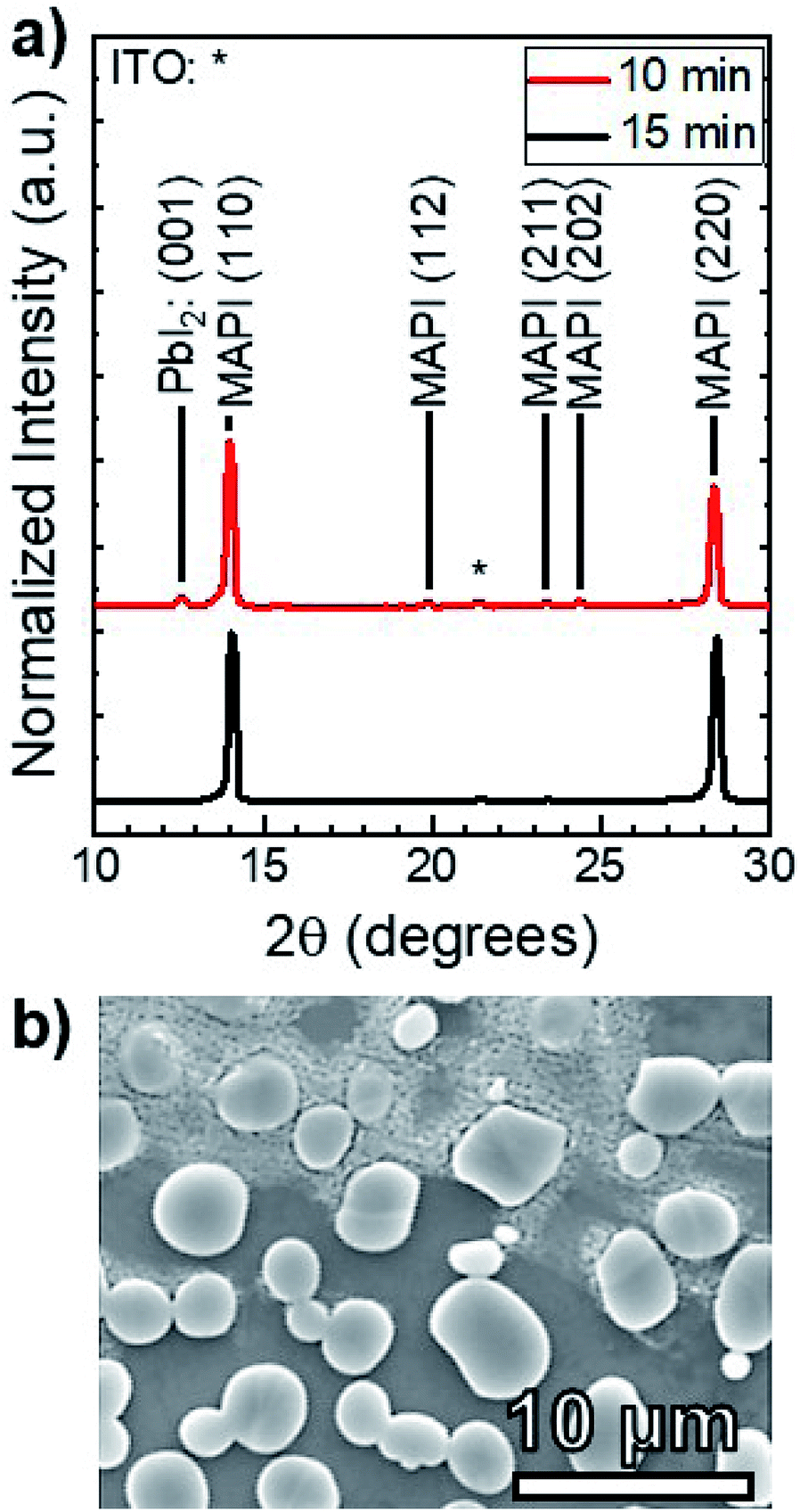 | ||
| Fig. 6 (a) XRD patterns of MAPI films reacted isothermally at T = 160 °C and P = 9 torr with durations of t = 10 min and t = 15 min. The PbI2 (001) peak and the tetragonal MAPI peaks are labeled. (b) A plan-view SEM micrograph of the 15 min-reacted MAPI film. | ||
Fig. 6b shows that the resulting MAPI films have a discontinuous morphology of large agglomerates on the substrate surface. EDS was used to characterize the films and confirmed that the light gray agglomerates were MAPI and the dark background was the SLG/ITO/CdS substrate. This agglomeration may be caused by de-wetting from the substrate surface during the reaction process—possibly due to high interfacial surface energy between the substrate and the perovskite. Alternatively, it may be due to Ostwald ripening where small, thermodynamically unstable particles are incorporated into larger, more stables particles to minimize interfacial surface energy.30 Both phenomena typically occur at elevated temperatures due to increased adatom mobility,31 and suggest that the 160 °C reaction temperature is too high for MAPI processing on CdS at P = 9 torr.
3.3 Characterization of solar cells
Fully-reacted MAPI films from 150 min reactions at 100 °C were integrated into functional solar cells with an SLG/ITO/CdS/MAPI/Spiro/Au structure as shown in the cross-sectional SEM image of Fig. 7. The MAPI and Spiro layers appear to form pinhole-free films with only small thickness variations due to the intrinsic roughness of the MAPI layer. The MAPI grains appear to be dense and columnar with a grain width of ≈150–200 nm. Furthermore, the reaction appears to have doubled the thickness of the original PbI2 film from ≈225 nm of PbI2 to ≈450 nm of MAPI.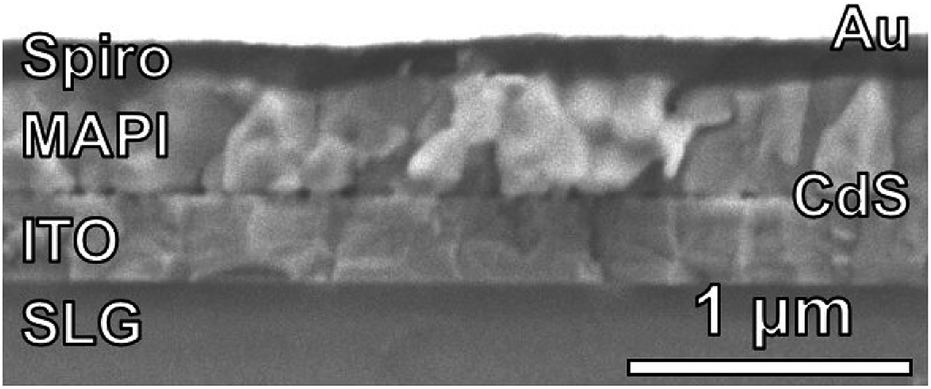 | ||
| Fig. 7 A cross-sectional SEM image of a completed device with an SLG/ITO/CdS/MAPI/Spiro/Au stack. | ||
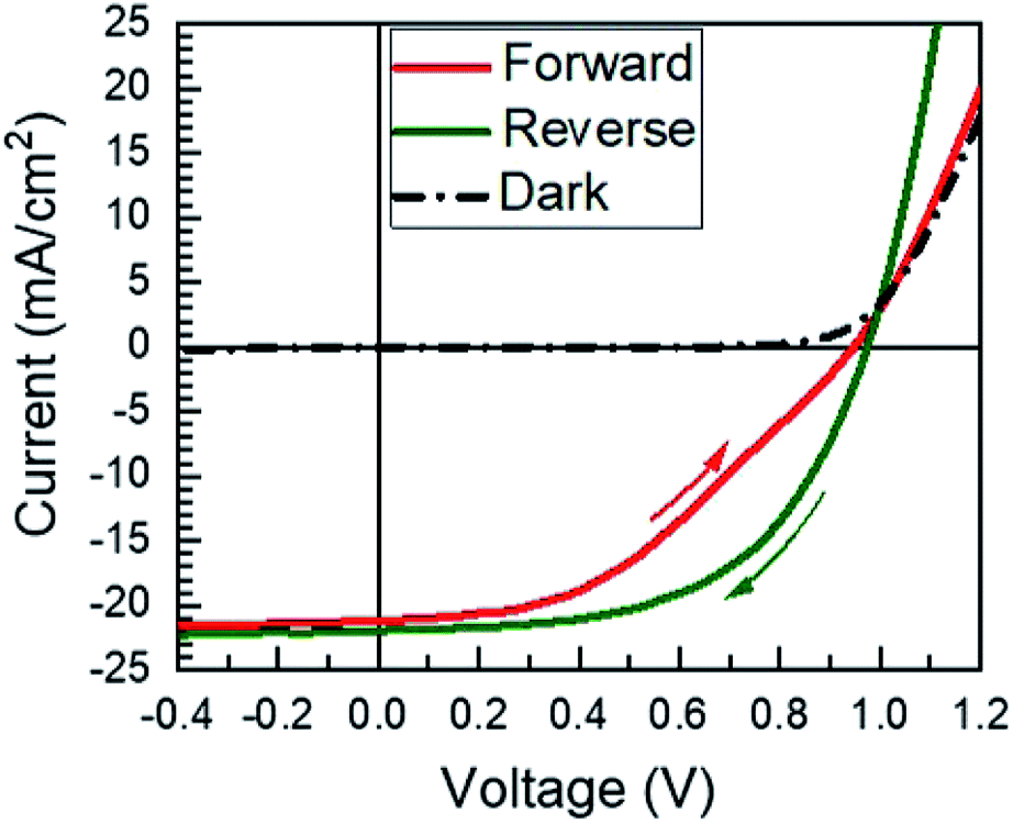
A total of 50 solar cells were fabricated with identical PbI2 deposition, MAI reaction, and device processing conditions. A champion cell performance of 12.1% efficiency was achieved on a reverse sweep with open-circuit voltage (VOC) = 980 mV, short-circuit current (JSC) = 21.9 mA cm−2, and fill factor (FF) = 56.6% as shown in Fig. 8. However, this device exhibited hysteresis as evidenced by a lower efficiency of 8.4% during the forward sweep. This lower efficiency is due primarily to a loss in FF with VOC = 950 mV, JSC = 21.1 mA cm−2, and FF = 41.9%. The higher performance in the reverse sweep is consistent with previous reports, which have attributed hysteretic effects to ion migration within the MAPI layer, where a positive voltage bias leads to better band alignment and improved carrier collection.32
 | ||
| Fig. 8 The JV curve of the champion solar cell presented in this work. The arrows indicate the direction of the scan. | ||
The compiled cell parameters for all 50 devices are shown in Table 1. On average these cells exhibit a reasonable VOC and JSC of 968 mV and 18.3 mA cm−2 that can be incrementally improved upon to achieve high efficiency solar cells. However, there are substantial losses in FF that limit the efficiency. These losses can be attributed primarily to the CdS electron transport layer because, in addition to parasitic absorption and a small conduction band spike,33 it has been reported that CdS can interact with excess MAI to form an interfacial Cd perovskite (MA2CdI4).34 This would create a blocking barrier and reduce both the JSC and the FF.34 Therefore, it is likely that replacing CdS with a more appropriate electron transport layer, such as SnO2 or TiO2, could be used to improve the FF and the overall cell efficiency.
| Parameter | Average | Standard deviation |
|---|---|---|
| VOC (mV) | 968 ± 6 | 20 |
| JSC (mA cm−2) | 18.3 ± 0.6 | 2.1 |
| FF (%) | 47.4 ± 1.4 | 5.0 |
| PCE (%) | 8.4 ± 0.3 | 1.1 |
4 Discussion
This all-vapor CSVT process serves as an advance toward developing a commercial vapor deposition method for the production of perovskite thin films. However, there are several concepts that must be better understood before designing and implementing scaled VTD reactors. First, the perovskite field has moved away from the CH3NH3PbI3 composition toward alloys that include formamidinium, Cs, and Br because they have proven to be more stable and more efficient.3 It is apparent that a commercial perovskite production process will require the flexibility and methods to incorporate alloys into the material. Second, a quantitative mass transport model of the vapor deposition process is necessary to develop a scaled-up process. The composition of the alloyed perovskite film is essential to its performance and stability; therefore, a model is needed to guide experimentation toward a targeted composition. Finally, VTD of perovskites could be carried out either via a sequential process, as illustrated through CSVT, or via a simultaneous process. While the sequential process is limited by the rate of PbI2 conversion, a sequential process could circumvent this issue by co-depositing the perovskite's constituent materials through a low-vacuum and high-throughput process. Any effort to address one of these outstanding issues would be of great importance in developing perovskite vapor processing at the commercial scale.5 Conclusions
This work establishes a sequential, all-vapor CSVT process to fabricate single-phase CH3NH3PbI3 perovskite thin films. Vapor-processed PbI2 films deposited on a CdS substrate possess a hexagonal, platelet-like morphology oriented about the (001) basal plane. Reacting these films at 100 °C and 9 torr produces continuous MAPI films, but this reaction temperature yields a slow reaction that requires at least 125 min to reach complete conversion. The change in PbI2 phase content versus time was used to quantify the rate of reaction, however further study is needed to develop a more accurate kinetic mechanism. Reacting the PbI2 films at 160 °C and 9 torr yields complete conversion to MAPI in 15 min, but this elevated reaction temperature promotes de-wetting from the substrate which inhibits the formation of a continuous MAPI film. Devices fabricated from MAPI processed at T = 100 °C in the configuration SLG/ITO/CdS/MAPI/Spiro/Au achieved a champion cell efficiency of 12.1% with VOC = 980 mV, JSC = 21.9 mA cm−2, and FF = 56.6%. These results validate CSVT as a viable processing technique for perovskite solar applications and establish a foundation for further research into scaling perovskite production through VTD.Conflicts of interest
There are no conflicts to declare.Acknowledgements
This material is supported in part by the Engineering Research Center Program of the National Science Foundation and the Solar Energy Technology Office of the Department of Energy under NSF Cooperative Agreement No. EEC-1041895. The authors also wish to acknowledge Shannon Fields for constructing the CSVT reactor, Wayne Buchanan for ITO and Au depositions, and Chris Thompson for assistance with JV setup and testing.Notes and references
- J. A. Christians, P. Schulz, J. S. Tinkham, T. H. Schloemer, S. P. Harvey, B. J. Tremolet De Villers, A. Sellinger, J. J. Berry and J. M. Luther, Nat. Energy, 2018, 3, 68–74 CrossRef CAS.
- G. Grancini, C. Roldán-Carmona, I. Zimmermann, E. Mosconi, X. Lee, D. Martineau, S. Narbey, F. Oswald, F. De Angelis, M. Graetzel and M. K. Nazeeruddin, Nat. Commun., 2017, 8, 1–8 CrossRef PubMed.
- M. Saliba, T. Matsui, J. Y. Seo, K. Domanski, J. P. Correa-Baena, M. K. Nazeeruddin, S. M. Zakeeruddin, W. Tress, A. Abate, A. Hagfeldt and M. Grätzel, Energy Environ. Sci., 2016, 9, 1989–1997 RSC.
- D. Yang, R. Yang, K. Wang, C. Wu, X. Zhu, J. Feng, X. Ren, G. Fang, S. Priya and S. F. Liu, Nat. Commun., 2018, 9, 3239 CrossRef PubMed.
- N. J. Jeon, H. Na, E. H. Jung, T. Y. Yang, Y. G. Lee, G. Kim, H. W. Shin, S. Il Seok, J. Lee and J. Seo, Nat. Energy, 2018, 3, 682–689 CrossRef CAS.
- E. H. Jung, N. J. Jeon, E. Y. Park, C. S. Moon, T. J. Shin, T. Y. Yang, J. H. Noh and J. Seo, Nature, 2019, 567, 511–515 CrossRef CAS PubMed.
- S. Razza, F. Di Giacomo, F. Matteocci, L. Cinà, A. L. Palma, S. Casaluci, P. Cameron, A. D'Epifanio, S. Licoccia, A. Reale, T. M. Brown and A. Di Carlo, J. Power Sources, 2015, 277, 286–291 CrossRef CAS.
- S. G. Li, K. J. Jiang, M. J. Su, X. P. Cui, J. H. Huang, Q. Q. Zhang, X. Q. Zhou, L. M. Yang and Y. L. Song, J. Mater. Chem. A, 2015, 3, 9092–9097 RSC.
- K. Hwang, Y. S. Jung, Y. J. Heo, F. H. Scholes, S. E. Watkins, J. Subbiah, D. J. Jones, D. Y. Kim and D. Vak, Adv. Mater., 2015, 27, 1241–1247 CrossRef CAS PubMed.
- B. Dou, J. B. Whitaker, K. Bruening, D. T. Moore, L. M. Wheeler, J. Ryter, N. J. Breslin, J. J. Berry, S. M. Garner, F. S. Barnes, S. E. Shaheen, C. J. Tassone, K. Zhu and M. F. Van Hest, ACS Energy Lett., 2018, 3, 2558–2565 CrossRef CAS.
- Y. Zhong, R. Munir, J. Li, M.-C. Tang, M. R. Niazi, K. Zhao and A. Amassian, ACS Energy Lett., 2018, 3, 1078–1085 CrossRef CAS.
- G. E. Eperon, S. D. Stranks, C. Menelaou, M. B. Johnston, L. M. Herz and H. J. Snaith, Energy Environ. Sci., 2014, 7, 982–988 RSC.
- L. Gil-Escrig, C. Momblona, M. G. La-Placa, P. P. Boix, M. Sessolo and H. J. Bolink, Adv. Energy Mater., 2018, 8, 1–6 Search PubMed.
- M. R. Leyden, L. K. Ono, S. R. Raga, Y. Kato, S. Wang and Y. Qi, J. Mater. Chem. A, 2014, 2, 18742–18745 RSC.
- C. Momblona, L. Gil-Escrig, E. Bandiello, E. M. Hutter, M. Sessolo, K. Lederer, J. Blochwitz-Nimoth and H. J. Bolink, Energy Environ. Sci., 2016, 9, 3456–3463 RSC.
- B. E. McCandless and J. R. Sites, in Handbook of Photovoltaic Science and Engineering, ed. A. Luque and S. Hegedus, John Wiley & Sons, Chichester, United Kingdom, 2nd edn, 2011, ch. 14, pp. 600–641 Search PubMed.
- G. Li, J. Y. L. Ho, M. Wong and H.-S. Kwok, Phys. Status Solidi RRL, 2016, 10, 153–157 CrossRef CAS.
- Q. Guo, C. Li, W. Qiao, S. Ma, F. Wang, B. Zhang, L. Hu, S. Dai and Z. Tan, Energy Environ. Sci., 2016, 9, 1486–1494 RSC.
- E. Pérez-Gutiérrez, M. J. Percino, D. M. Montoya, D. Solis-Ibarra, M. Cerón and O. Barbosa-García, ACS Appl. Energy Mater., 2018, 3843–3849 CrossRef.
- R. J. Konings, E. H. Cordfunke, J. E. Fearon and R. R. Van Der Laan, Thermochim. Acta, 1996, 273, 231–238 CrossRef CAS.
- A. Dualeh, P. Gao, S. I. Seok, M. K. Nazeeruddin and M. Grätzel, Chem. Mater., 2014, 26, 6160–6164 CrossRef CAS.
- G. Tong, Z. Song, C. Li, Y. Zhao, L. Yu, J. Xu, Y. Jiang, Y. Sheng and K. Chen, RSC Adv., 2017, 7, 19457–19463 RSC.
- B. E. McCandless and W. N. Shafarman, Proceedings of the 3rd World Conference on Photovoltaic Energy Conversion, Osaka, 2003, pp. 562–565 Search PubMed.
- M. Saliba, J. P. Correa-Baena, C. M. Wolff, M. Stolterfoht, N. Phung, S. Albrecht, D. Neher and A. Abate, Chem. Mater., 2018, 30, 4193–4201 CrossRef CAS.
- W. A. Rachinger, J. Sci. Instrum., 1948, 25, 254–255 CrossRef.
- H. Klug and L. Alexander, X-ray Diffraction Procedures For Polycrystalline and Amorphous Materials, John Wiley & Sons, New York, 2nd edn, 1954 Search PubMed.
- Q. Lin, A. Armin, R. C. R. Nagiri, P. L. Burn and P. Meredith, Nat. Photonics, 2015, 9, 106–112 CrossRef CAS.
- D. Liu, M. K. Gangishetty and T. L. Kelly, J. Mater. Chem. A, 2014, 2, 19873–19881 RSC.
- P. A. Beckmann, Cryst. Res. Technol., 2010, 45, 455–460 CrossRef CAS.
- M. Grundmann, The Physics of Semiconductors, Springer US, New York, 3rd edn, 2016 Search PubMed.
- D. L. Smith, Thin Film Deposition: Principles and Practice, McGraw-Hill, Inc., New York, 1995 Search PubMed.
- C. Eames, J. M. Frost, P. R. Barnes, B. C. O'Regan, A. Walsh and M. S. Islam, Nat. Commun., 2015, 6, 7494 CrossRef PubMed.
- S. Bansal and P. Aryal, 2017 IEEE 44th Photovoltaic Specialist Conference, PVSC 2017, 2017, pp. 1–4 Search PubMed.
- W. A. Dunlap-Shohl, R. Younts, B. Gautam, K. Gundogdu and D. B. Mitzi, J. Phys. Chem. C, 2016, 120, 16437–16445 CrossRef CAS.
| This journal is © The Royal Society of Chemistry 2020 |