 Open Access Article
Creative Commons Attribution 3.0 Unported Licence
SiO2 thin film growth through a pure atomic layer deposition technique at room temperature†
D. Arl *,
V. Rogé,
N. Adjeroud,
B. R. Pistillo
 ,
M. Sarr,
N. Bahlawane
 and
D. Lenoble
Luxembourg Institute of Science and Technology, 41 rue du Brill, L-4422, Luxembourg. E-mail: didier.arl@list.lu
First published on 11th May 2020
Abstract
In this study, less contaminated and porous SiO2 films were grown via ALD at room temperature. In addition to the well-known catalytic effect of ammonia, the self-limitation of the reaction was demonstrated by tuning the exposure of SiCl4, NH3 and H2O. This pure ALD approach generated porous oxide layers with very low chloride contamination in films. This optimized RT-ALD process could be applied to a wide range of substrates that need to be 3D-coated, similar to mesoporous structured membranes.
Introduction
Silicon dioxide (SiO2) and more generally ultra-thin oxide films have been extensively described as good components for modern nanotechnologies such as dielectric materials in silicon microelectronic devices,1,2 anticorrosion films3 or non-exhaustive applications of nanoscale films in catalysis. The environment- and human-friendly nature of SiO2 induces its wide use in protective layers for antisticking, antifogging, self-cleaning or water repellency.4–7 Various techniques such as chemical vapor deposition,8 lithographic patterning,9 electrochemical deposition10 or sol–gel11,12 were investigated to prepare superhydrophobic SiO2 by tuning surface roughness or energy. SiO2 is consistently known for its application in protective or gate insulator coatings13 and interfacing high-k (ref. 14–19) or surface passivation materials.20–23 The increased demand for transparent active materials at the nanoscale justify the need for a deposition technique compatible with sensitive pre-deposited underlying layers, flexible plastic devices or high aspect ratio substrates.24–28 Therefore, atomic layer deposition (ALD) is considered as one of the most suitable techniques for its performance in terms of sub-nanometer thickness control and penetration coating into deep trenches or mesoporous structures.SiO2 thin films obtained through ALD have widely been described as binary surface reactions dealing with various types of precursors Si(C2H5O)4,29 SiCl4 (ref. 13 and 30–33) or Si(NCO)4 (ref. 34) with H2O; CH3OSi(NCO)3 (ref. 35 and 36) with H2O2; Si(NCH3)2)4, ((CH3)2N)3SiH37 or SiH2(NEt2)2 (ref. 38)). Besides the necessity to work at high temperatures (i.e. >100–350 °C), most of the reactions require large reactant exposure of ≥109 L (1 L = 10−6 Torr s) with a growth rate of59 ∼1–2 Å per cycle.39 One approach to decrease the deposition temperature and the level of contamination is to use plasma-enhanced-ALD (PE-ALD).40,58,59 It is possible to decrease the temperature below 50 °C, and these SiO2 films are described as excellent candidates for thin film encapsulation in organic devices or TFT gate insulators due to the absence of impurities and good electrical properties.41–43,60 Currently, the use of amino ligands as precursors leads to promising results, even on large surfaces; however, a final annealing step at 900–1000 °C is required to decrease interface defects or carbon contamination.44,45 Many efforts have been done, in terms of parameters and choice of precursors, in order to optimise ALD process, for the growth of SiO2 coatings at high temperatures. Nevertheless, it is commonly agreed that there is a strong interest in the development of the process at room temperature. George et al. described the atomic layer-controlled growth using SiCl4 and H2O many times.13,31,44,46 They demonstrated that a reaction catalyzed using Lewis bases such as pyridine (C5H5N) or ammonia (NH3) avoids large precursor flow rates and can only occur close to room temperature. Nevertheless, in these studies, C5H5N or NH3 were never really considered as “precursors”. The proposed mechanism, which took into account the hydrogen bonding between the Lewis base and either the SiOH* surface species or the H2O reactant, was studied by considering the global residual pressure of the continuous flow of the catalyst. Moreover, the secondary reaction of the catalyst reservoir (continuous flow), available in the reactor with HCl as the byproduct, drastically increased the probability of the inclusion of contaminants in the film. Therefore, a sequential approach could enhance the quality of the film and the understanding of the role of the catalyst.
This paper describes a pure ALD study of SiO2 using the optimized sequential exposure of SiCl4, H2O and NH3(g) precursors at room temperature. The ALD mode was confirmed by tuning the exposition of each precursor and the related purges. The initiation of the exposition was followed by using the residual gas analysis (RGA) mass spectrometer. Atomic growth control was investigated by the in situ Quartz Crystal Microbalance (QCM) and X-ray Photoelectron Spectroscopy (XPS), Dynamic-Secondary Mass Ion Spectroscopy (D-SIMS) and X-ray Diffraction (XRD) post-characterizations. A comparison between our investigation and the state-of-the-art of low temperature ALD SiO2 synthesis revealed the possibility to deposit ultra-thin films with very low contaminations at room temperature. The film conformality is shown and the capability of this optimized binary reaction, to be used on various types of temperature-sensitive supports with high aspect ratios, is confirmed.
Materials and methods
ALD processes were carried out in a TFS200-Beneq reactor in the planar configuration at a base pressure of 0.3 mbar. SiO2 thin films were then deposited on Si substrates, preliminary prepared by a standardized cleaning procedure established by Radio Corporation of America (RCA). The deposition reactor was equipped with a QCM (Neyco) for the gravimetric monitoring of the film growth. The QCM was fixed to the central part of the substrate holder. A quadrupole mass spectrometer, Vision-2000C, MKS-instrument, was assembled at the outlet of the deposition reactor to monitor the exhaust gas composition. SiO2 thin films were obtained at room temperature using SiCl4 and H2O as precursors. The vaporized precursors were transferred to the ALD reaction chamber with N2 as the carrier gas. SiCl4 was purchased from Sigma Aldrich and used as-received. Both canisters containing the precursors were maintained at 19 °C during deposition. NH3 gas (<99.9%), used as a catalyst, was injected into the reactor under 1 bar pressure.The morphology and thickness of the obtained samples were characterized using a FEI Heliosnanolab 650 Focused Ion Beam Secondary Electron Microscope (FIB-SEM). The structure of the films deposited on dedicated Kapton tape was probed by small-angle X-ray scattering (SAXS) using an X-ray Diffractometer (X'Pert Pro (Panalytical)) equipped with a focusing mirror and a Pixcel 1D detector in the transmission mode. The elemental composition depth profile was assessed using D-SIMS (Cameca, IMSLAM); however, the quantification was performed by XPS (Thermo VG Scientific, MicroLab 350) using Al Kα source.
Results and discussion
Catalytic SiO2 RT-ALD growth
SiO2 films obtained at room temperature have already been prepared by the sequential exposure (ABAB…) of two reactants (A and B). Many well-known precursors require high deposition temperatures, plasma or highly reactive co-reactants such as ozone gas.47 Despite a low enthalpy of reaction, SiCl4 usually reacts with water (oxidant species) at high temperatures (>325 °C).13 The comparison of thermal ALD and room temperature processes reveals a higher growth rate/ALD cycle in favour of room temperature reactions (∼2 Å per cycle) (Fig. S1, ESI†).The amount of contaminants integrated in RT-SiO2 films is inherently dependent on the way of tuning the surface exposure to precursors. Based on studies by George et al.,31 we investigated the growth of SiO2 at room temperature (RT)-ALD by alternatively exposing the surface to SiCl4 and H2O under a constant flow of NH3. The exposure time was fixed at 90 s for SiCl4 with a purge time of 1 min. H2O exposure was fixed at 90 s with a purge time of 5 min to ensure a perfect saturation of the surface.31 The in situ monitoring of the film growth obtained by the QCM is shown in Fig. S2, ESI.† As already described,31 the reduction reaction of SiCl4 with water is depicted through the minimum of SiCl4 weight gain (Fig. S2b, ESI†) and the longer reaction of the NH3–H2O mixture (Fig. S2c–e, ESI†). Then, as shown in Fig. S2b, ESI,† the gain of mass that is observed in one ALD cycle is predominantly obtained from the half reaction of H2O. Nevertheless, the growth rate of ∼1.5 Å per cycle (297 nm/2000 cycles), experimentally obtained through this process with a constant flow of NH3, tends to reach the 2 Å per cycle value described by George et al.31
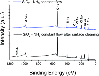
XPS elemental analysis of the SiO2 film (deposited on Al2O3/Si) (Fig. 1) shows the presence of carbon, nitrogen and chlorine in addition to silicon and oxygen within the SiO2 deposited film. A depth profiling analysis reveals that the carbon is restricted to the surface of the film.
The asymmetry of the C 1s peak suggests the presence of C–H, C–O–C or C![[double bond, length as m-dash]](https://www.rsc.org/images/entities/char_e001.gif) O bonds at the surface due to air exposure. The Si 2p peak of the Si–O layer appeared at 104.4 eV with a 1.77 eV (broadened up to 2.22 eV due to charge effects during the depth profiling) full width at half maximum (FWHM). The sharp and symmetric Si 2p peak centred at ∼104 eV suggests an oxidation state of +1, which was attributed to the presence of SiO2. A high contribution of the byproducts of the reaction is detected through the presence of Cl and N elements in the films. The Si/Cl ratio increased from ∼1.3 at the surface to 3.2 in the bulk of the film (Table 1).
O bonds at the surface due to air exposure. The Si 2p peak of the Si–O layer appeared at 104.4 eV with a 1.77 eV (broadened up to 2.22 eV due to charge effects during the depth profiling) full width at half maximum (FWHM). The sharp and symmetric Si 2p peak centred at ∼104 eV suggests an oxidation state of +1, which was attributed to the presence of SiO2. A high contribution of the byproducts of the reaction is detected through the presence of Cl and N elements in the films. The Si/Cl ratio increased from ∼1.3 at the surface to 3.2 in the bulk of the film (Table 1).
| Name | At% | At% (depth profiling) |
|---|---|---|
| Si 2p | 17.6 | 29.5 |
| O 1s | 45.9 | 47.7 |
| N 1s | 16.5 | 13.5 |
| Cl 2p | 13.6 | 9.1 |
| C 1s | 6.4 | <1 |
Furthermore, the reaction of the lone pair of active –Cl with the hydrogen of water induced a significant formation of HCl. The higher detection limit of D-SIMS was used to screen the chemical elements present in the “bulk” of the film, particularly for light elements such as hydrogen. As shown in Fig. 2, all typical elements of the deposited film, i.e. Si, O, Cl, N, H and C, are detected. The intensity of Cl is similar to that of Si and O while a difference in the intensity is observed for H, N and C. It can be seen from the depth profile analysis that the signal of C decreases rapidly, which is in agreement with the XPS results. As H% is roughly constant, the slow decrease in N and Cl tends to confirm that a part of the film is composed of NH4Cl contaminants.
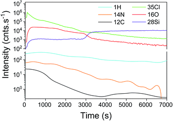 | ||
| Fig. 2 SIMS depth profile of the SiO2 film obtained with a constant flow of NH3. A thickness of 297 nm is calculated by the sputtering time. | ||
Contaminant inclusion mechanism
George et al. described the mechanism of a catalysed binary reaction that spontaneously takes place in the presence of pyridine or NH3 as a Lewis base agent.30,48 The hydrogen bonding between the Lewis base and SiOH* (surface species) or H2O allows the reaction to be performed at room temperature (Fig. S3, ESI†). Compared to high temperature processes that use large precursor exposures (>103 Torr s), SiO2 RT-ALD takes place owing to the strong nucleophilic attack of the oxygen from (i) Si![[O with combining low line]](https://www.rsc.org/images/entities/char_004f_0332.gif) H* on SiCl4 and that from (ii) H2O on SiCl*.46 Nevertheless, to the best of our knowledge, no specific data have been reported on the variation of the chemical composition and the morphology of such films. Based on the catalytic effect of NH3, it can be clearly deduced that a constant flow of NH3 statistically ensures a maximized reaction of –O on all –O–Si–(Cl)n available sites. Nevertheless, the perfect delimitation of the exposure windows at room temperature could be enhanced by working in a non-conventional high vacuum state (<10−6 Torr). As it is not the case for standard ALD reactors, we attempted to understand and control the contaminant inclusion mechanism in the pulsed NH3 regime. Thus, the state-of-the-art production of SiO2 at RT using a constant flow of NH3 has been compared to pulse NH3-catalysed RT-ALD. Inspired by the reactivity of chlorinated precursors described by Damyanov et al.,49 the amount of contamination could be cautiously explained by the functionality x of the adsorbed species at the surface explained hereafter:
H* on SiCl4 and that from (ii) H2O on SiCl*.46 Nevertheless, to the best of our knowledge, no specific data have been reported on the variation of the chemical composition and the morphology of such films. Based on the catalytic effect of NH3, it can be clearly deduced that a constant flow of NH3 statistically ensures a maximized reaction of –O on all –O–Si–(Cl)n available sites. Nevertheless, the perfect delimitation of the exposure windows at room temperature could be enhanced by working in a non-conventional high vacuum state (<10−6 Torr). As it is not the case for standard ALD reactors, we attempted to understand and control the contaminant inclusion mechanism in the pulsed NH3 regime. Thus, the state-of-the-art production of SiO2 at RT using a constant flow of NH3 has been compared to pulse NH3-catalysed RT-ALD. Inspired by the reactivity of chlorinated precursors described by Damyanov et al.,49 the amount of contamination could be cautiously explained by the functionality x of the adsorbed species at the surface explained hereafter:x(![[triple bond, length as m-dash]](https://www.rsc.org/images/entities/char_e002.gif) Si–OH) + SiCl4 → ( Si–OH) + SiCl4 → (![[triple bond, length as m-dash]](https://www.rsc.org/images/entities/char_e002.gif) Si–O)xSiCl4−x + xHCl Si–O)xSiCl4−x + xHCl |
The injected precursor SiCl4 reacted with the surface (![[triple bond, length as m-dash]](https://www.rsc.org/images/entities/char_e002.gif) ) hydroxyl species. Moreover, the competition between the single bond case (x = 1) and multiple bonds (1 < x ≤ 3) was directly linked to the stagnancy of precursors in the ALD regime. As far as the concentration of hydroxyl groups on the surface increased, the saturation of H2O directly enhanced the formation of HCl. Along with the constant flow of NH3, the ∼2.2 Si/N ratio measured by XPS in the bulk of the film indicates a strong nitrogen contamination exceeding acceptable limits, especially through the inclusion of NH4Cl salt. As indicated by George et al.,31 this salt is formed as a result of the NH3 catalyst complexing with HCl. Because of the vapour pressure of the NH4Cl salt (i.e. 4 × 10⁻⁵ Torr (ref. 50)), some quantity of the salt remained within the film. In that context, note that compared to an inert gas, using NH3 as a carrier gas may not contribute to a pure ALD process performed at RT. Indeed, a significant contamination of the surface is attributed to the excessive dose of NH3. The contamination depicted here confirms the already described importance of adjusting the quantity of NH3 to limit the reaction with HCl.31 Thus, we considered that pulsing NH3 similar to the other precursors could minimize unfavourable reactions at room temperature.
) hydroxyl species. Moreover, the competition between the single bond case (x = 1) and multiple bonds (1 < x ≤ 3) was directly linked to the stagnancy of precursors in the ALD regime. As far as the concentration of hydroxyl groups on the surface increased, the saturation of H2O directly enhanced the formation of HCl. Along with the constant flow of NH3, the ∼2.2 Si/N ratio measured by XPS in the bulk of the film indicates a strong nitrogen contamination exceeding acceptable limits, especially through the inclusion of NH4Cl salt. As indicated by George et al.,31 this salt is formed as a result of the NH3 catalyst complexing with HCl. Because of the vapour pressure of the NH4Cl salt (i.e. 4 × 10⁻⁵ Torr (ref. 50)), some quantity of the salt remained within the film. In that context, note that compared to an inert gas, using NH3 as a carrier gas may not contribute to a pure ALD process performed at RT. Indeed, a significant contamination of the surface is attributed to the excessive dose of NH3. The contamination depicted here confirms the already described importance of adjusting the quantity of NH3 to limit the reaction with HCl.31 Thus, we considered that pulsing NH3 similar to the other precursors could minimize unfavourable reactions at room temperature.
Low contamination SiO2 growth under pulsed NH3
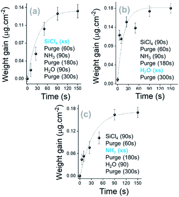 | ||
| Fig. 3 Saturation curves of SiCl4, H2O and NH3 along the SiO2 thin film growth. The kinetic growth is shown for 5 cycles with sequential exposure of the surface. | ||
Based on the trends observed in Fig. 4, the growth of a SiO2 film in a pure ALD regime at RT has been investigated. SiCl4, NH3 and H2O exposure times were fixed at 90 s and extended purges were applied after NH3 and H2O pulses at 180 s and 300 s, respectively. As shown in Fig. S5a, ESI,† the 0.02 μg cm−2 per cycle weight gain is 30 times lower than the process with a constant flow of NH3 (Fig. S2, ESI†). Nevertheless, the injection of NH3 and H2O precursors significantly contributes to a certain gain of mass (Fig. S5 panel b, ESI†), and then a growth rate of 0.5 Å per cycle is obtained for 500 deposition cycles. It can be observed that the high H2O mass adsorbed during the interaction of H2O molecules with active complexes at the surface ends through the efficient replacement of chlorine by hydroxyl groups (Fig. S3, ESI†).
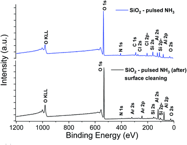
The XPS elemental analysis (Fig. 4) still shows the presence of chlorine, nitrogen and carbon in addition to silicon and oxygen. The amount of contaminants (Table 2) is nonetheless substantially decreased. Firstly, the Si/Cl ratio increased from ∼4 (surface) to ∼8.7 in the bulk of the film. Secondly, compared to the films obtained with a constant flow of ammonia, the Si/Cl ratio improved significantly (threefold). Moreover, the Si/N ratio increased from 1.1 to 3.8 (2.2 to 5.9 inside the film). This indicates a limited reaction between HCl and NH3 to form NH4Cl. The best fitting procedure of the high-resolution spectrum of N 1s reveals a single binding energy peak at 401.1 ± 0.3 eV, corresponding to NH3+. This confirms the formation of the NH4Cl salt, and the small amount of detected Al is attributed to the alumina sub-layer (i.e. SiO2/Al2O3/Si).
| Name | At% | At% (depth profiling) |
|---|---|---|
| Si 2p | 12.9 | 4.1 |
| O 1s | 54.2 | 59.7 |
| N 1s | 3.6 | 0.7 |
| Cl 2p | 3.2 | 0.5 |
| C 1s | 11.4 | <1.0 |
| Al 2p | 14.7 | 34.9 |
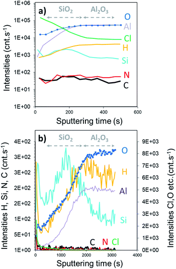
The SIMS depth profile of the SiO2 film is shown in Fig. 5. The intensity of chlorine decreases ∼30 times faster than the process performed with the constant NH3 flow. In fact, less than 100 s sputtering is needed to decrease the intensity below 1 × 10⁵ cnts per s compared to ∼2800 s for the NH3 constant flow process. Moreover, the intensity of nitrogen seems to be in the same range of 10–100 cnts per s. Compared to the XPS results, this corroborates the formation of the NH4Cl salt. Note that the intensity of Si is higher than that of Al, confirming the coating process of SiO2 on Al2O3. From the depth profile, we can estimate the SiO2 film thickness to be around 25 nm. Based on the XPS and SIMS results, it can be assumed that this RT process is optimized in terms of surface exposure. Nevertheless, the residual traces of HCl still react with NH3 because of the difficulties to purge H2O or NH3 at RT. Moreover, small quantities of byproducts, such as NH4Cl, were consequently integrated into the film.
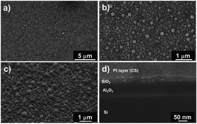
Fig. 6a and b show top-view SEM images of the SiO2 film. We observed a rough layer with grain sizes of up to 200 nm. This roughness is highlighted in the 45° tilted view (Fig. 6c).
Furthermore, cross-section analyses evidence the presence of a compact film (Fig. 6d). From these pictures, we can conclude that this pulsed NH3 growth process leads to dense but rough SiO2 thin films. A thickness of 30 ± 5 nm is measured through the cross-section, close to the 25 nm value deduced from the SIMS analysis. This leads to a lower growth rate of ∼0.5 Å per cycle related to the lower weight gain observed with QCM (i.e. 30× lower than the SiO2 film processed under a constant flow of NH3). Nevertheless, the irregular surface aspect reveals that the process does not correspond to a pure ALD growth mode, as expected.51–53 This peculiar non-homogeneous growth at RT suggests that the surface reaction is in competition with the integration of contaminants. The self-limiting process actually promotes the deposition of species onto the substrate and onto the deposits (e.g. islands) with equal probability.54–56 The inclusion of contaminants at a sub-atomic growth rate (i.e. <1 Å per cycle) could explain the morphology of the obtained film. Moreover, the high amount of –OH surface groups could affect the dehydroxylation/rehydroxylation equilibrium (section: Contaminant inclusion mechanism), leading to the production of a higher quantity of HCl in the case of trifunctional bonds. Nevertheless, the oxide thin film displays a significant density in volume with limited inhomogeneity. This is in line with the sub-atomic growth rate mechanism surrounded by limited contamination. The tailoring of ALD parameters in this RT-SiO2 growth process shows a substantial adaptability in terms of morphology and chemical composition. These results suggest that a tuning of the growth parameters could influence the crystallisation. Hence, different types of SiO2 layers could be processed at RT.
As shown in Fig. S6, ESI,† a growth rate of 1.54 μg cm−2 per cycle was obtained. Compared to the process described in the previous section, the exposure reaction used here generates ∼50 times higher weight gain. In order to disentangle any physico-chemical influence from the substrate, silicon oxide films were grown on a pre-characterized barrier layer. Hence, SiO2 growth was investigated on two different sub-layers, i.e. TiO2 deposited by ALD and Si bulk.
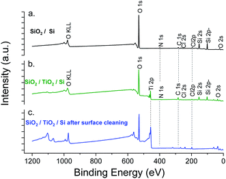
Fig. 7 shows the XPS experiment results. As expected, Cl, C, N elements were detected in both samples. For SiO2 deposited on TiO2, the detection of Ti 2p before etching confirms the low thickness of the film.
However, the percentage of chlorine was clearly maintained below the limit of 3% (obtained for the previous process with extended exposures) (Table 3). The higher chlorine concentration observed after etching (3.79 at%) was attributed to the chlorine inherent to the TiO2 ALD process. This was confirmed by the low chlorine concentration for SiO2 deposited directly on the silicon wafer (Table 3, SiO2/Si). In order to screen the composition and morphology of the film, thicker SiO2 layer (2500 cycles) were processed on a chlorine-free material, i.e. Al2O3 (50 nm) on Si.
| Name | At% | At% (depth profiling) |
|---|---|---|
| SiO2/TiO2/Si | ||
| Si 2p | 16.4 | — |
| O 1s | 58.8 | 63.4 |
| N 1s | 1.4 | — |
| Cl 2p | 1.1 | 3.8 |
| C 1s | 14.6 | — |
| Ti 2p | 7.7 | 32.8 |
![[thin space (1/6-em)]](https://www.rsc.org/images/entities/char_2009.gif) |
||
| SiO2/Si | ||
| Si 2p | 25.9 | 34.4 |
| O 1s | 60.5 | 62.9 |
| N 1s | 1.6 | 2.3 |
| Cl 2p | 1.0 | 0.5 |
| C 1s | 11.1 | <1 |
The SIMS depth profiling of the synthesized SiO2 thick film exhibits a concentration of chlorine that rapidly decreases as a function of sputtering time (Fig. 8). Compared to the previous process, the intensity of Cl is starting a decade less, around 3.5 × 10⁴ cnts per s. Moreover, the amount of C and N is very low, which confirms the low level of NH4Cl contamination in a thick volume of SiO2.
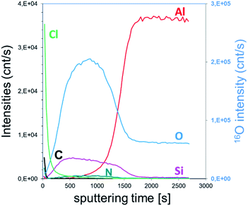 | ||
| Fig. 8 SIMS depth profile of porous SiO2 film obtained with 100 ms pulse of SiCl4, 2s of NH3 and H2O precursors. | ||
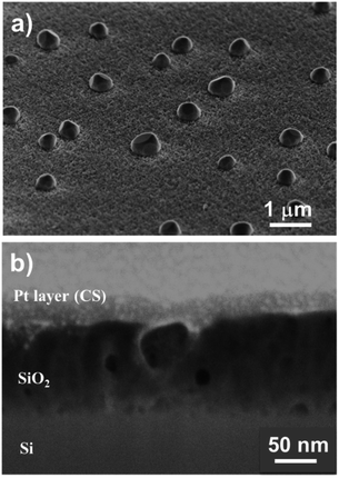
Furthermore, the higher concentration of chlorine close to the surface of the film indicated the slow dissociative chemisorption of water, which induced the desorption of HCl. This recombination clearly affected the growth mechanism of SiO2. As shown in Fig. 9, SEM analyses highlighted the porous state of the oxide film. In addition to the 200–500 nm diameter aggregates on the surface of the layer, the top and tilted view (Fig. 9a) revealed a SiO2 sponge-like structure. The porosity of the film was confirmed by SAXS where a periodical arrangement of pores could be fitted with an average radius of 130 Å (std dev 30% and most frequent radius ∼ 110 Å). The applied FIB cross-section (Fig. 9b) reveals the presence of 20–50 nm cavities (merging pores due to the preparation) and isolated pores of ∼15 nm. As explained by Puurunen in the ALD random deposition approach,56 if the growth per cycle is not constant, the increase in the surface roughness should be fast at the beginning of the growth and slow thereafter. This naturally indicates that a smaller number of ALD reaction cycles are required to fit a conformal deposition in a close-packed array as far as the growth rate is adjacent to an atomic monolayer.
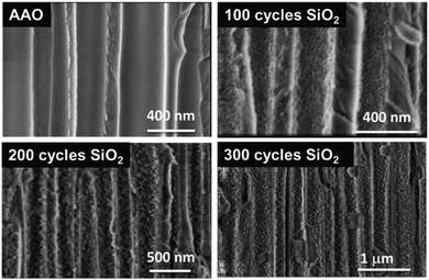
By considering the growth rate of ∼0.11 Å per cycle obtained in this process, it could explain why the SiO2 film is less “closed” as the one processed via the pure ALD approach. The sponge-like porous structure growth may be related to the limited surface diffusion of the by-products (NH4Cl, HCl) generated during each half cycle. Indeed, the diffusion/desorption of byproducts is slower in the case of low reaction temperature (here RT) and short purge time. In this case, residual water or byproducts (NH4Cl, HCl) are considered as surface fractions where the supplementary amount of the injected precursor will be adsorbed instead of the –Si–OH surface groups. This prevents the growth of SiO2 and leads to non-uniform porous thin films. Nevertheless, this peculiar structure is very attractive for applications that need to be processed at RT. Even if other techniques such as PE-ALD are able to produce SiO2 dense thin films with no impurities at reduced temperatures (50–80 °C) for specific applications,41–43,57 we evidenced our ability to fabricate a highly porous SiO2 layer at room temperature with a significant level of control of the contamination. This specific characteristic of this porous SiO2 layer is clearly transferred to complex and temperature-sensitive 3D materials. Hence, ALD SiO2 could be deposited in a porous anodic aluminum oxide (AAO) membrane, and the results are shown in Fig. 10. It clearly appears that the porosity obtained on planar substrates is perfectly transferable to 3D surfaces. This suggests that the ALD technique for SiO2 thin film synthesis could be applied to any 3D complex substrate. Further studies are in progress.
Conclusions
Porous SiO2 thin films have been produced by ALD using a sequential exposure of SiCl4, NH3 and H2O at room temperature. The catalytic effect of ammonia has been exploited to optimize the saturation of the precursors and the extended purges. A relation between the significant porosity and the chemical saturation of the surface has been indicated using QCM, XPS, SIMS and SEM. It has also been demonstrated that this optimized process exhibited a decrease in the inherent inclusion of contaminants such as NH4Cl and HCl in the film. As demonstrated on AAO membranes, the transferability of this 2D process to 3D structures could extend the use of SiO2 films in several domains such as complex or high aspect ratio materials.Conflicts of interest
The authors disclose that there are there are no conflicts to declare.Acknowledgements
The authors would like to acknowledge le Fond National de la Recherche (FNR) of Luxembourg for the financial support. The authors are very grateful to Ms. Diana Li, Ms. Anne-Catherine Fischer and Mr Jerome Guillot for their scientific contribution.References
- C. J. Frosch and L. Derick, Surface Protection and Selective Masking during Diffusion in Silicon, J. Electrochem. Soc., 1957, 104(9), 547–552 CrossRef CAS.
- S. Wolf and R. N. Tauber, Deep Sub-micron process technology. Lattice Press, CA, 1986 Search PubMed.
- C. O. A. Olsson and D. Landolt, Passive films on stainless steels chemistry, structure and growth, Electrochim. Acta, 2003, 48(9), 1093–1104 CrossRef CAS.
- C. G. Granqvist, Transparent conductors as solar energy materials: A panoramic review, Sol. Energy Mater. Sol. Cells, 2007, 91(17), 1529–1598 CrossRef CAS.
- J. A. Howarter and J. P. Youngblood, Self-Cleaning and Anti-Fog Surfaces via Stimuli-Responsive Polymer Brushes, Adv. Mater., 2007, 19(22), 3838–3843 CrossRef CAS.
- T. Kako, et al., Adhesion and sliding of wet snow on a super-hydrophobic surface with hydrophilic channels, J. Mater. Sci., 2004, 39(2), 547–555 CrossRef CAS.
- L. Y. L. Wu, et al., Quantitative test method for evaluation of anti-fingerprint property of coated surfaces, Appl. Surf. Sci., 2011, 257(7), 2965–2969 CrossRef CAS.
- P. Ragesh, et al., A review on self-cleaning and multifunctional materials', J. Mater. Chem. A, 2014, 2(36), 14773–14797 RSC.
- H. K. Park, S. W. Yoon and Y. R. Do, Superhydrophobicity of 2D SiO2 hierarchical micro/nanorod structures fabricated using a two-step micro/nanosphere lithography, J. Mater. Chem., 2012, 22(28), 14035–14041 RSC.
- Y. Gao, et al., Highly Transparent and UV-Resistant Superhydrophobic SiO2-Coated ZnO Nanorod Arrays, ACS Appl. Mater. Interfaces, 2014, 6(4), 2219–2223 CrossRef CAS PubMed.
- B. Xu, et al., Preparation of superhydrophobic cotton fabrics based on SiO2 nanoparticles and ZnO nanorod arrays with subsequent hydrophobic modification, Surf. Coat. Technol., 2010, 204(9–10), 1556–1561 CrossRef CAS.
- Y. Zheng, et al., Formation of SiO2/polytetrafluoroethylene hybrid superhydrophobic coating, Appl. Surf. Sci., 2012, 258(24), 9859–9863 CrossRef CAS.
- J. W. Klaus, O. Sneh and S. M. George, Growth of SiO2 at Room Temperature with the Use of Catalyzed Sequential Half-Reactions, Science, 1997, 278(5345), 1934–1936 CrossRef CAS PubMed.
- C. C. Fulton, G. Lucovsky and R. J. Nemanich, Process-dependent band structure changes of transition-metal (Ti,Zr,Hf) oxides on Si (100), Appl. Phys. Lett., 2004, 84(4), 580–582 CrossRef CAS.
- X. Wang, et al., Comprehensive understanding of the effect of electric dipole at high-k/SiO2 interface on the flatband voltage shift in metal-oxide-semiconductor device, Appl. Phys. Lett., 2010, 97(6), 062901–062903 CrossRef.
- K. Kita and A. Toriumi, Origin of electric dipoles formed at high-k/SiO2 interface, Appl. Phys. Lett., 2009, 94(13), 132902–132903 CrossRef.
- X. Wang, et al., Electric Dipole at High-k/SiO2 Interface and Physical Origin by Dielectric Contact Induced Gap States, Jpn. J. Appl. Phys., 2011, 50(10), 10PF02 CrossRef.
- C. Kirkpatrick, et al., Performance improvement of AlGaN/GaN high electron mobility transistors with atomic layer deposition (ALD) of SiO2 and HfAlO dielectrics, Phys. Status Solidi C, 2011, 8(7–8), 2445–2447 CrossRef CAS.
- B. Lee, et al., Normally-off AlGaN/GaN MOSHFET using ALD SiO2 tunnel dielectric and ALD HfO2 charge storage layer for power device application, Phys. Status Solidi C, 2012, 9(3–4), 868–870 CrossRef CAS.
- G. Dingemans, M. C. M. van de Sanden and W. M. M. Kessels, Excellent Si surface passivation by low temperature SiO2 using an ultrathin Al2O3 capping film, Phys. Status Solidi RRL, 2011, 5(1), 22–24 CrossRef CAS.
- G. Dingemans, et al., Controlling the fixed charge and passivation properties of Si(100)/Al2O3 interfaces using ultrathin SiO2 interlayers synthesized by atomic layer deposition, J. Appl. Phys., 2011, 110(9), 093715–093716 CrossRef.
- G. Dalapati, et al., Surface Passivation of GaAs Substrates with SiO2 Deposited Using ALD, Electrochem. Solid-State Lett., 2011, 14(10), G52–G55 CrossRef CAS.
- H. Guo, et al., High-performance GaN-based light-emitting diodes on patterned sapphire substrate with a novel hybrid Ag mirror and atomic layer deposition-TiO2/Al2O3 distributed Bragg reflector backside reflector, Opt. Eng., 2013, 52(6), 063402 CrossRef.
- H. Kim and P. McIntyre, Atomic Layer Deposition of Ultrathin Metal-Oxide Films for Nano-Scale Device Applications, J. Korean Phys. Soc., 2006, 48, 5–17 CAS.
- L. Giordano and G. Pacchioni, Oxide Films at the Nanoscale: New Structures, New Functions, and New Materials, Acc. Chem. Res., 2011, 44(11), 1244–1252 CrossRef CAS PubMed.
- K. E. Elers, et al., Film Uniformity in Atomic Layer Deposition, Chem. Vap. Deposition, 2006, 12(1), 13–24 CrossRef CAS.
- S. M. George, Atomic Layer Deposition: An Overview, Chem. Rev., 2009, 110(1), 111–131 CrossRef PubMed.
- H. Kim and P. C. McIntyre, Atomic layer deposition of ultrathin metal-oxide films for nano-scale device applications, J. Korean Phys. Soc., 2006, 48(1), 5–17 CAS.
- J. D. Ferguson, et al., ALD of SiO at Room Temperature Using TEOS and H2O with NH3 as the Catalyst, J. Electrochem. Soc., 2004, 151(8), G528–G535 CrossRef CAS.
- J. W. Klaus, et al., Atomic layer deposition of SiO2 using catalysed and uncatalysed self-limiting surface reactions, Surf. Rev. Lett., 1999, 6(3–4), 435–448 CrossRef CAS.
- J. W. Klaus and S. M. George, Atomic layer deposition of SiO2 at room temperature using NH3-catalyzed sequential surface reactions, Surf. Sci., 2000, 447(1–3), 81–90 CrossRef CAS.
- B. A. McCool and W. J. DeSisto, Self-Limited Pore Size Reduction of Mesoporous Silica Membranes via Pyridine-Catalyzed Silicon Dioxide ALD, Chem. Vap. Deposition, 2004, 10(4), 190–194 CrossRef CAS.
- B. A. McCool and W. J. DeSisto, Synthesis and Characterization of Silica Membranes Prepared by Pyridine-Catalyzed Atomic Layer Deposition, Ind. Eng. Chem. Res., 2004, 43(10), 2478–2484 CrossRef CAS.
- W. Gasser, Y. Uchida and M. Matsumura, Quasi-monolayer deposition of silicon dioxide, Thin Solid Films, 1994, 250(1–2), 213–218 CrossRef CAS.
- S. Morishita, Y. Ushida and M. Matsumura, Atomic-Layer Chemical-Vapor-Deposition of SiO2 by Cyclic Exposures of CH3OSi(NCO)3 and H2O2, Jpn. J. Appl. Phys., 1995, 34, 5738–5742 CrossRef CAS.
- S. Morishita, et al., New substances for atomic-layer deposition of silicon dioxide, J. Non-Cryst. Solids, 1995, 187, 66–69 CrossRef CAS.
- M. Degai, et al., Non-heating atomic layer deposition of SiO2 using tris(dimethylamino)silane and plasma-excited water vapor, Thin Solid Films, 2012, 525, 73–76 CrossRef CAS.
- J. Lim, S. Yun and J. Lee, Low-Temperature Growth of SiO2 Films by Plasma-Enhanced Atomic Layer Deposition, ETRI Journal, 2005, 27(1), 118–121 CrossRef.
- B. B. Burton, et al., Rapid SiO2 Atomic Layer Deposition Using Tris(tert-pentoxy)silanol, Chem. Mater., 2008, 20(22), 7031–7043 CrossRef CAS.
- T. Nam, et al., Low-temperature, high-growth-rate ALD of SiO2 using aminodisilane precursor, Appl. Surf. Sci., 2019, 485, 381–390 CrossRef CAS.
- J. Sheng, et al., Performance and Stability Enhancement of In–Sn–Zn–O TFTs Using SiO2 Gate Dielectrics Grown by Low Temperature Atomic Layer Deposition, ACS Appl. Mater. Interfaces, 2017, 9(49), 42928–42934 CrossRef CAS PubMed.
- J.-H. Lee, et al., Plasma enhanced atomic layer deposited silicon dioxide with divalent Si precursor [N,N′-tert-butyl-1,1-dimethylethylenediamine silylene], Appl. Surf. Sci., 2019, 493, 125–130 CrossRef CAS.
- Y. Lee, et al., Effects of O2 plasma treatment on moisture barrier properties of SiO2 grown by plasma-enhanced atomic layer deposition, Ceram. Int., 2019, 45(14), 17662–17668 CrossRef CAS.
- G. Dingemans, et al., Plasma-Assisted ALD for the Conformal Deposition of SiO2: Process, Material and Electronic Properties, J. Electrochem. Soc., 2012, 159(3), H277–H285 CrossRef CAS.
- D. Hiller, et al., Low temperature silicon dioxide by thermal atomic layer deposition: Investigation of material properties, J. Appl. Phys., 2010, 107(6), 064314 CrossRef.
- Y. Du, X. Du and S. M. George, SiO2 film growth at low temperatures by catalyzed atomic layer deposition in a viscous flow reactor, Thin Solid Films, 2005, 491(1–2), 43–53 CrossRef CAS.
- H.-U. Kim and S.-W. Rhee, Electrical Properties of Bulk Silicon Dioxide and SiO2/Si Interface Formed by Tetraethylorthosilicate-Ozone Chemical Vapor Deposition, J. Electrochem. Soc., 2000, 147(4), 1473–1476 CrossRef CAS.
- O. Sneh, et al., Atomic layer growth of SiO2 on Si(100) using SiCl4 and H2O in a binary reaction sequence, Surf. Sci., 1995, 334(1–3), 135–152 CrossRef CAS.
- D. Damyanov, et al., On the mechanism of interaction between TiCl4 vapour and surface OH groups of amorphous SiO2, J. Non-Cryst. Solids, 1988, 105(1–2), 107–113 CrossRef CAS.
- CRC Handbook of Chemistry and Physics, CRC Press, Boca Raton, FL, 63rd edn 1984 Search PubMed.
- T. Suntola, Atomic layer epitaxy, Mater. Sci. Rep., 1989, 4(5), 261–312 CrossRef CAS.
- T. Suntola, Atomic layer epitaxy, Thin Solid Films, 1992, 216(1), 84–89 CrossRef CAS.
- M. Ritala, et al., Perfectly Conformal TiN and Al2O3 Films Deposited by Atomic Layer Deposition, Chem. Vap. Deposition, 1999, 5(1), 7–9 CrossRef CAS.
- Y. Kajikawa, S. Noda and H. Komiyama, Use of process indices for simplification of the description of vapor deposition systems, Mater. Sci. Eng., B, 2004, 111(2–3), 156–163 CrossRef.
- R. L. Puurunen, Formation of metal oxide particles in atomic layer deposition during the chemisorption of metal chlorides: A review, Chem. Vap. Deposition, 2005, 11(2), 79–90 CrossRef CAS.
- R. L. Puurunen, Random Deposition as a Growth Mode in Atomic Layer Deposition, Chem. Vap. Deposition, 2004, 10(3), 159–170 CrossRef CAS.
- Y.-J. Choi, et al., Robust SiO2 gate dielectric thin films prepared through plasma-enhanced atomic layer deposition involving di-sopropylamino silane (DIPAS) and oxygen plasma: Application to amorphous oxide thin film transistors, Ceram. Int., 2018, 44(2), 1556–1565 CrossRef CAS.
- K. Pfeiffer, Comparative study of ALD SiO2 thin films for optical applications, Opt. Mater. Express, 2016, 6(2), 660–670 CrossRef CAS , https://www.osapublishing.org/ome/abstract.cfm?URI=ome-6-2-660.
- V. Beladiya, Effect of an electric field during the deposition of silicon dioxide thin films by plasma enhanced atomic layer deposition: an experimental and computational study, Nanoscale, 2020, 12(3), 2089–2102 RSC.
- P. Paul, Antireflection Coating on PMMA Substrates by Atomic Layer Deposition, Coatings, 2020, 10(1), 64–77 CrossRef CAS , https://www.mdpi.com/2079-6412/10/1/64.
Footnote |
| † Electronic supplementary information (ESI) available. See DOI: 10.1039/d0ra01602k |
| This journal is © The Royal Society of Chemistry 2020 |

