
 Open Access Article
 This Open Access Article is licensed under a
 Creative Commons Attribution 3.0 Unported Licence
Effects of alkali and transition metal-doped TiO2 hole blocking layers on the perovskite solar cells obtained by a two-step sequential deposition method in air and under vacuum†
U. Nwankwoabcd,
Siphelo Ngqolodae,
Agnes C. Nkelea,
Christopher J. Arendse e,
Kenneth I. Ozoemenaf,
A. B. C. Ekwealora,
Rajan Joseg,
Malik Maazacd and
Fabian I. Ezema*acd
e,
Kenneth I. Ozoemenaf,
A. B. C. Ekwealora,
Rajan Joseg,
Malik Maazacd and
Fabian I. Ezema*acd
aDepartment of Physics and Astronomy, University of Nigeria Nsukka, Nigeria. E-mail: fabian.ezema@unn.edu.ng
bDepartment of Physics/Geology/Geophysics, Alex Ekwueme Federal University Ndufu-Alike, Ikwo, Nigeria
cNanosciences African Network (NANOAFNET), iThemba LABS-National Research Foundation, 1 Old Faure Road, Somerset West 7129, P.O. Box 722, Somerset West, Western Cape Province, South Africa
dUNESCO-UNISA Africa Chair in Nanosciences/Nanotechnology, College of Graduate Studies, University of South Africa (UNISA), Muckleneuk Ridge, P.O. Box 392, Pretoria, South Africa
eDepartment of Physics and Astronomy, University of the Western Cape, Private Bag X17, Bellville, 7535, South Africa
fMolecular Sciences Institute, School of Chemistry, University of the Witwatersrand, Private Bag 3, P O Wits, Johannesburg 2050, South Africa
gNanostructured Renewable Energy Materials Laboratory, Faculty of Industrial Sciences and Technology, Universiti Malaysia Pahang, 26300 Kuantan, Pahang, Malaysia
First published on 1st April 2020
Abstract
Planar perovskite solar cells (PPSCs) have received great attention in recent years due to their intriguing properties, which make them a good choice for photovoltaic applications. In this work, the effect of alkali and transition metal-doped TiO2 (cesium-doped TiO2 (Cs-TiO2) and yttrium-doped TiO2 (Y-TiO2)) compact layers on the optical, structural and the photovoltaic performance of the PPSCs have been investigated. The perovskite layer syntheses were carried out by depositing a lead iodide (PbI2) layer via spin-coating; converting PbI2 into methyl ammonium iodide (CH3NH3PbI3) by chemical vapor deposition (CVD) and spin-coating at 60 min and 60 s conversion times respectively. The as-deposited PPSCs were studied layer-by-layer using an X-ray diffractometer, scanning electron microscope, and UV-vis diffuse reflectance, transmittance and absorbance. The power conversion efficiency for stable processed perovskite solar cells were 3.61% and 12.89% for air and vacuum processed, respectively.
1. Introduction
Perovskite solar cells (PSCs) have attracted great interest due to their intriguing properties such as large absorption coefficient, high electron–hole diffusion length, tunable band gap, high charge carrier mobility, low temperature processing and low cost of production. These have made them good choices as efficient multi-purpose photovoltaics (PVs) for the next generation PV devices. The power conversion efficiency (PCE) of PSCs has been improved from 9.7%1 to 22.1%2–4 in the last seven years. The main device architectures of PCSs have been presented as planar and mesoporous, and are made up of the perovskite absorber layer, electron transport layer (ETL) and hole transport layer (HTL)5–7 on a fluorine-doped tin oxide (FTO) substrate. In the planar architecture, the perovskite absorber (CH3NH3PbI3) is usually sandwiched between ETL and HTL without a mesoporous layer while mesoporous architecture includes a mesoporous layer. Newly emerging device architectures are the inverted planar PSCs and planar structure PSCs without HTL.8,9 The perovskite absorber layer is the brain box of the perovskite photovoltaic devices where the charge carriers (excitons) are generated when light of energy greater than or equal to the optical bandgap of the absorber layer. Due to weak binding energy of the exciton (electron–hole), the separation of these electrons–holes take place at room temperature and requires an instant transport to ETL and HTL under the internal electric field at the junction.10 However, failure to transport the photo-generated charge carriers to the appropriate transport layer may result to quick recombination, charge accumulation at the interface and reduction in charge transfer.11–13 Due to the above mentioned reasons, efficient ETL is required to effectively extract the electron from the active layer before recombination occurs. A compact ETL, which is one component of the planar PSCs structure, has shown to be the most promising in producing a high and stable PCE. The planar structure without a mesoporous layer improves the perovskite crystallinity, surface morphology and reduce charge recombination.14–16In the recent years, numerous metal oxides have been employed to improve the effectiveness of electron transport materials (ETM) such as titanium oxide (TiO2), aluminum oxide (Al2O3), zinc oxide (ZnO), tin oxide (SnO2), and magnesium oxide (MgO)17–21 etc. TiO2 has been proven to be the most widely preferred ETM due to its chemical stability, low-cost synthesis and charge transport tendency.10,22,23 In addition, TiO2 ETM has shown a better conversion efficiency, and this is possible due to the band alignment between the conduction band of the TiO2 ETL and the lower unoccupied molecular orbital (LUMO) perovskite active layer.24 The electrons generated in the absorber layer can make his way to the ETL with less stress. Despite all these good names given to TiO2, it suffers from poor to low electrical conductivity. There is need to improve the electrical conductivity for better electron transport efficiency. One of the adopted ways to improve the electrical conductivity of the TiO2 ETL is metal ion doping. TiO2 metal ion doping have been reported in which several metal dopants such as lanthanum, lithium, niobium, aluminum and magnesium, were used for mesoporous doping on the TiO2 layer.25,26 The incorporation of these metal dopants resulted in tuning the Fermi level, reduced electronic trap sites, enhanced optical band gap and improved stability of the PSCs.27–29
Compact-TiO2 (c-TiO2) layer is the most frequently used ETL in the fabrication of highly efficient PSCs because of several reasons such as better exciton separation, easy to process in air, high transparency and low cost of fabrication.30 Varieties of deposition methods have been used in the preparation of c-TiO2 layer as ETL in PSCs, like spin-coating, dip-coating, spray-coating, magnetron sputtering, electrochemical deposition, electron beam deposition and atomic layer deposition.31–34 Spin-coating presents a lot of advantages over other deposition technique such as easy fabrication, low energy intensive, and thin film control through precursor concentration.35 The desired thickness of c-TiO2 layer is in the range of 10–80 nm for planar structure without mesoporous TiO2 layer. However, optimization of c-TiO2 layer for use as ETL in PSCs is currently an area of research that has received a great attention. The c-TiO2 layer is crucial by selectively allowing the electron generated at the absorber layer to be extracted to the electrode (FTO) so as to block the hole at the junction between FTO/absorber layer.36,37 It helps also to prevent carrier recombination at the perovskite/absorber interface, pinhole-free and maximum light penetration. Moreover, doped c-TiO2 layer have been reported to address the issue of hysteresis.38 More works are required to further improve the solar parameters and stability of planar (with no mesoporous layer) PSCs.
In this study, Cs and Y doped c-TiO2 ETL have been synthesized by sol–gel spin-coating deposition, which further promotes cost reduction of the PSCs. The planar architecture (n–i–p structure), FTO/doped c-TiO2/CH3NH3PbI3/HTL/Ag were used in all the fabrication steps. We further studied the crystal structure, electrical conductivity, optical properties, and layer-by-layer surface morphology of PSCs with the active layer deposited by two-step vapour deposition method. The PCE for perovskite layer deposited by spin coating and CVD methods was compared for different c-TiO2. The effects of the doped c-TiO2 and the active layer deposition technique on the performance of the fabricated PSCs were discussed in the article. Moreover, this research work addresses the issue of choice of deposition method for doped c-TiO2 ETL and the perovskite absorber layer on the PSCs performance.
2. Experimental
2.1 Materials
The materials used for this study were purchased as commercial products and some were used as purchased without any further purification. Methyl ammonium iodide (CH3NH3I), unpatterned FTO coated glass substrates (10 ohm per sq), 2,2′′,7,7′′-tetrakis(N,N-di-p-methoxyphenylamine)-9,9-spirobifluorene (Spiro-MeOTAD) were purchased at the Ossila. Lead(II) iodide (PbI2; 99%), titanium isopropoxide (TTIP; 97%), chlorobenzene, 4-tert-butylpyridine (tBP), acetonitrile (99.8%), lithium bis-(trifluoromethanesulfonyl)imide (LITSFI), N,N-dimethylformamide (DMF; 99.8%), and dimethyl sulfoxide (DMSO; 99.9%) were purchased from Sigma and ALDRICH.2.2 Preparation of c-TiO2 pristine and doped c-TiO2 layer
Prior to the deposition of c-TiO2 layer used in this study, the unpatterned FTO substrates were patterned by etching the desired portion with zinc (Zn) powder and 2 M hydrochloric acid (HCl). The etched substrates were cleaned in Hellmanex detergent, sonicated in deionized water (70 °C), isopropanol (IPA) and deionized water (70 °C) respectively. The cleaned FTO patterned substrates were treated by UV-O3 for 10 min.The c-TiO2 layers were deposited on the patterned FTO substrates by sol–gel spin coating at 3000 rpm for 30 s, preheated for 10 min at 30 °C slightly above room temperature, and finally calcined at 400 °C for 1 h using hot plate. The titanium precursor solutions were prepared by adding different masses of cesium chloride (CsCl) and yttrium(III) oxide (Y2O3) in ethanol (2.5 mL) and stirred for 2 h to dissolve completely. 350 μL of TTIP in ethanol (2.5 mL; 99.9%) in separate beaker was stirred for 10 min to form a milky solution. An acidic solution was prepared in a different beaker by adding 2 drops of HCl (2 M) in ethanol (2.5 mL). The dopant solution and acidic solution were added to the titanium precursor under constant stirring to clear the milky solution and form a viscous colorless solution. The prepared sol was spin-coated on the FTO patterned substrate by masking the undesired area for metal contact with acid resistive tape to form a thin FTO/c-TiO2. The same method was repeated for pristine c-TiO2 without adding any dopant oxides.
2.3 Fabrication of the perovskite absorber layer
The perovskite absorber layer was prepared by two-step spin-coating and two-step chemical vapor deposition method. The schematic diagram of the deposition steps is shown in Fig. 1.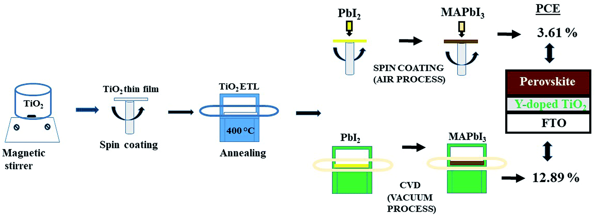 | ||
| Fig. 1 Schematic diagram of the deposition steps for the perovskite solar cell. | ||
![[thin space (1/6-em)]](https://www.rsc.org/images/entities/char_2009.gif) :1 respectively to form 0.8 M PbI2 solution. The PbI2 solution was heated at 65 °C for 3 h with the bottle containing the solution capped for the PbI2 to dissolve properly. With the PbI2 solution kept at 65 °C, 40 μL of the dissolved PbI2 solution was spin-coated on the FTO/c-TiO2 and FTO/c-TiO2 substrate which was heated at 65 °C prior to deposition at 7000 rpm for 35 s. The spin-coated PbI2 layer was preheated at 40 °C for 4 min, and finally heated at 105 °C for 4 min for the solvent to evaporate. This first procedure for the preparation of MAPbI3 by spin-coating is considered as the first step while the second step is to convert the PbI2 layer into MAPbI3. The conversion of the PbI2 into MAPbI3 was done by dissolving 10 mg of CH3NH3I in 1 mL of IPA, and then dropped on the PbI2 layer to diffuse into the layer for 60 s (loading time), followed by spin-coating at 4000 rpm for 20 s. The converted MAPbI3 was dried at 105 °C for 2 min to obtain a dark brown perovskite layer film. Afterwards, 50 μL of HTL (Spiro-OMeTAD) solution was spin coated on the MAPbI3 layer at 300 rpm for 30 s after which the perovskite layer was cooled to room temperature. The Spiro-OMeTAD solution was made from the mixture of 180 mg of 2,2′′,7,7′′-tetrakis(N,N-di-p-methoxyphenylamine)-9,9-spirobifluorene (Spiro-OMeTAD) in 1 mL of chlorobenzene, 30 μL of 4-tert-butylpyridine (tBP) and 20 μL of lithium bis-(trifluoromethanesulfonyl)imide (LITSFI) solution (520 mg of LITSFI in 1 mL of acetonitrile) stirred for 30 min and allow overnight to oxidize. Finally, 100 nm in thickness of silver (Ag) electrodes were deposited at a deposition rate of 0.1 Å s−1 using thermal evaporator to form a FTO/c-TiO2/MAPbI3/Spiro-OMeTAD/Ag device.
:1 respectively to form 0.8 M PbI2 solution. The PbI2 solution was heated at 65 °C for 3 h with the bottle containing the solution capped for the PbI2 to dissolve properly. With the PbI2 solution kept at 65 °C, 40 μL of the dissolved PbI2 solution was spin-coated on the FTO/c-TiO2 and FTO/c-TiO2 substrate which was heated at 65 °C prior to deposition at 7000 rpm for 35 s. The spin-coated PbI2 layer was preheated at 40 °C for 4 min, and finally heated at 105 °C for 4 min for the solvent to evaporate. This first procedure for the preparation of MAPbI3 by spin-coating is considered as the first step while the second step is to convert the PbI2 layer into MAPbI3. The conversion of the PbI2 into MAPbI3 was done by dissolving 10 mg of CH3NH3I in 1 mL of IPA, and then dropped on the PbI2 layer to diffuse into the layer for 60 s (loading time), followed by spin-coating at 4000 rpm for 20 s. The converted MAPbI3 was dried at 105 °C for 2 min to obtain a dark brown perovskite layer film. Afterwards, 50 μL of HTL (Spiro-OMeTAD) solution was spin coated on the MAPbI3 layer at 300 rpm for 30 s after which the perovskite layer was cooled to room temperature. The Spiro-OMeTAD solution was made from the mixture of 180 mg of 2,2′′,7,7′′-tetrakis(N,N-di-p-methoxyphenylamine)-9,9-spirobifluorene (Spiro-OMeTAD) in 1 mL of chlorobenzene, 30 μL of 4-tert-butylpyridine (tBP) and 20 μL of lithium bis-(trifluoromethanesulfonyl)imide (LITSFI) solution (520 mg of LITSFI in 1 mL of acetonitrile) stirred for 30 min and allow overnight to oxidize. Finally, 100 nm in thickness of silver (Ag) electrodes were deposited at a deposition rate of 0.1 Å s−1 using thermal evaporator to form a FTO/c-TiO2/MAPbI3/Spiro-OMeTAD/Ag device.The procedures for HTL deposition layer and metal contact were repeated the same as the devices prepared by spin-coating technique to complete the device.
3. Characterization
The structural characterization of the synthesized TiO2 nanoparticles was carried out by an automatic powder X-ray diffractometer (XRD) X′ pert Pro with a theta–theta goniometer, using an ultrafast semiconductor detector pixel and Cu-Kα radiation (λ = 1.54 Å). The optical band gap, transmittance and absorbance were carried out with the Agilent Cary 5000 UV-VIS-NIR universal measurement spectrophotometer. The surface morphology and cross section imaging of the component layers were studied by Carl Zeiss mA 10 model field emission scanning electron microscopy (SEM) in combination with the energy dispersive X-ray spectroscopy (EDX) for elemental microanalysis. The current density–voltage (J–V) characteristics was measured with Keithley 2420 source meter under standard simulated solar irradiation of 1000 W m−2 (100 mW cm−2) and AM 1.5 at room temperature. The active area of the solar cell was 0.0512 cm2 as defined by the shadow mask used for the solar testing.4. Results and discussion
4.1 Thickness optimization of Cs and Y doped TiO2 on FTO substrate
The desired thickness for the compact Cs-and Y-doped TiO2 layer was between 20 and 80 nm. The prepared solution of Cs-and Y-doped TiO2 was controlled by the spin speed, spin time, atmospheric temperature, stirring speed and time in order to achieve the thickness in the desired range. The deposition of the TiO2 layers were performed using 40 μL of the solution, spin speed of 3000 rpm and spin time of 30 s to achieve the desired average thickness of 54 ± 5 nm. Table 1 shows the summary of the obtained thicknesses with respect to spin-coated growth conditions.| Amount of solution (μL) | Spin speed (rpm) | Spin duration (s) | Thickness (nm) |
|---|---|---|---|
| 40.0 | 3000.0 | 30.0 | 48.0, 56.5 and 58.5 |
| 80.0 | 3000.0 | 30.0 | 130.0 and 142.0 |
| 40.0 | 2000.0 | 60.0 | 58.8, 71.0 and 53.0 |
| 100.0 | 3000.0 | 40.0 | 140.0 and 150.0 |
| 150.0 | 2000.0 | 60.0 | 2000.0 |
The above thicknesses were achieved at room temperature deposition using static spin-coating technique and measured with Dektak Profilometer.
4.2 XRD characterization
Fig. 2 shows the XRD patterns for the pristine, doped Cs- and Y-TiO2 (Fig. 2(a)), perovskite layer processed in air (Fig. 2(b)) and vacuum (Fig. 2(c)).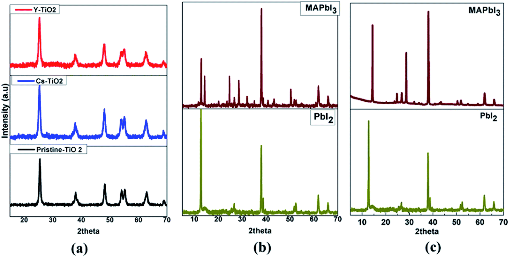 | ||
| Fig. 2 XRD Spectra of (a) pristine and doped TiO2 and (b) PbI2–MAPbI3 layer by spin-coating (c) PbI2–MAPbI3 layer by CVD. | ||
The XRD patterns of the dried titanium precursor annealed at 500 °C for 30 min for the pristine, Cs- and Y-doped TiO2 show anatase phase of TiO2. The diffraction peaks observed at 2theta (indexed) values: 25.28° (101), 38.57° (112), 48.05° (200), 53.89° (105), 55.06° (211), 62.69° (204), and 68.76° (116) (as shown in Fig. 2(a)) indicates an anatase with body-centered tetragonal structure of TiO2 (JCP2-021-1272) with lattice parameters of a = b = 3.78520 Å, c = 9.51390 Å. The calculated lattice parameters for pristine TiO2, Cs-doped TiO2 and Y-doped TiO2 are (a = b = 3.7739 Å, c = 9.2928 Å), (a = b = 3.7858 Å, c = 9.5087 Å), and (a = b = 3.7898 Å, c = 9.4407 Å) respectively.
There is no other TiO2 phase observed in the XRD patterns of the samples which were all crystallized at 500 °C annealing.
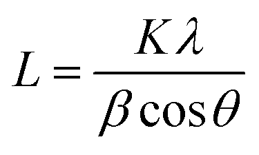
The crystallite size of the pristine, Cs- and Y-doped TiO2 particles were estimated by the Scherer's equation;40
 | (1) |
The XRD pattern of the spin-coated PbI2 layer and converted MAPbI3 perovskite on the compact pristine, Cs- and Y-doped TiO2 layer are as shown in Fig. 2(b). The XRD spectra of the PbI2 layers show main peaks at 2theta diffraction angle of 12.72° corresponding to the reflection from (001) plane, with a hexagonal crystal structure (JCPDS 07-0235). The crystallite size was calculated using the Scherer eqn (1) and estimated to be approximately 42 ± 3 nm.
MAPbI3 was obtained from the conversion of PbI2 as shown in the XRD pattern in Fig. 2(b) [MAPbI3]. After the transformation process of PbI2 to MAPbI3 was completed, new sets of diffraction peaks (2theta) related to the tetragonal perovskite structure appeared at 14.20°, 19.95°, 28.79°, 31.88°, 40.72°, and 43.15° corresponding to (110), (112), (004), (312), (224), and (314) crystal planes respectively. The crystallite size using the 110 peak located at 14.20° was calculated to be 81 ± 3 nm and was larger than the size of PbI2 before conversion to MAPbI3. These MAPbI3 peaks are accompanied by other peaks from PbI2 and FTO layers, in which the PbI2 peak appearing at 12.72° was an indication that the conversion had some remnant PbI2 in the perovskite layer. There is no impurity peak from both the first and second step deposition of perovskite layer. The XRD patterns of the perovskite layers were the same for the perovskite layer on pristine, Cs- and Y-doped TiO2. However, the XRD pattern of the perovskite layer grown by CVD is shown in Fig. 2(c). The XRD pattern of the PbI2 layer grown by CVD is similar to the one grown by spin-coating with the main peak appeared at 12.70° diffraction angle corresponding to (001) Bragg reflection plane of the PbI2 crystal structure. The conversion of PbI2 to MAPbI3 results to a new set of major peaks at the 2theta diffraction position 14.04°, 24.40° and 28.37° corresponding to (110), (202) and (220) reflection planes. The XRD pattern of perovskite absorber layer was improved as no remnant PbI2 peak appear on the diffraction pattern. This show that the conversion from PbI2 to MAPbI3 for perovskite absorber layer grown by CVD was completely done, while for spin-coating some remnant PbI2 not converted was present in the MAPbI3 diffraction peaks.
4.3 SEM and EDX analyses of ETL, perovskite active and HTL layers
The SEM micrograph of the top-view of the electron transporting layer (ETL), perovskite layer by spin-coating, hole transporting layer and perovskite layer by CVD are shown in Fig. 3(a–f) respectively and cross-sectional view in Fig. 4.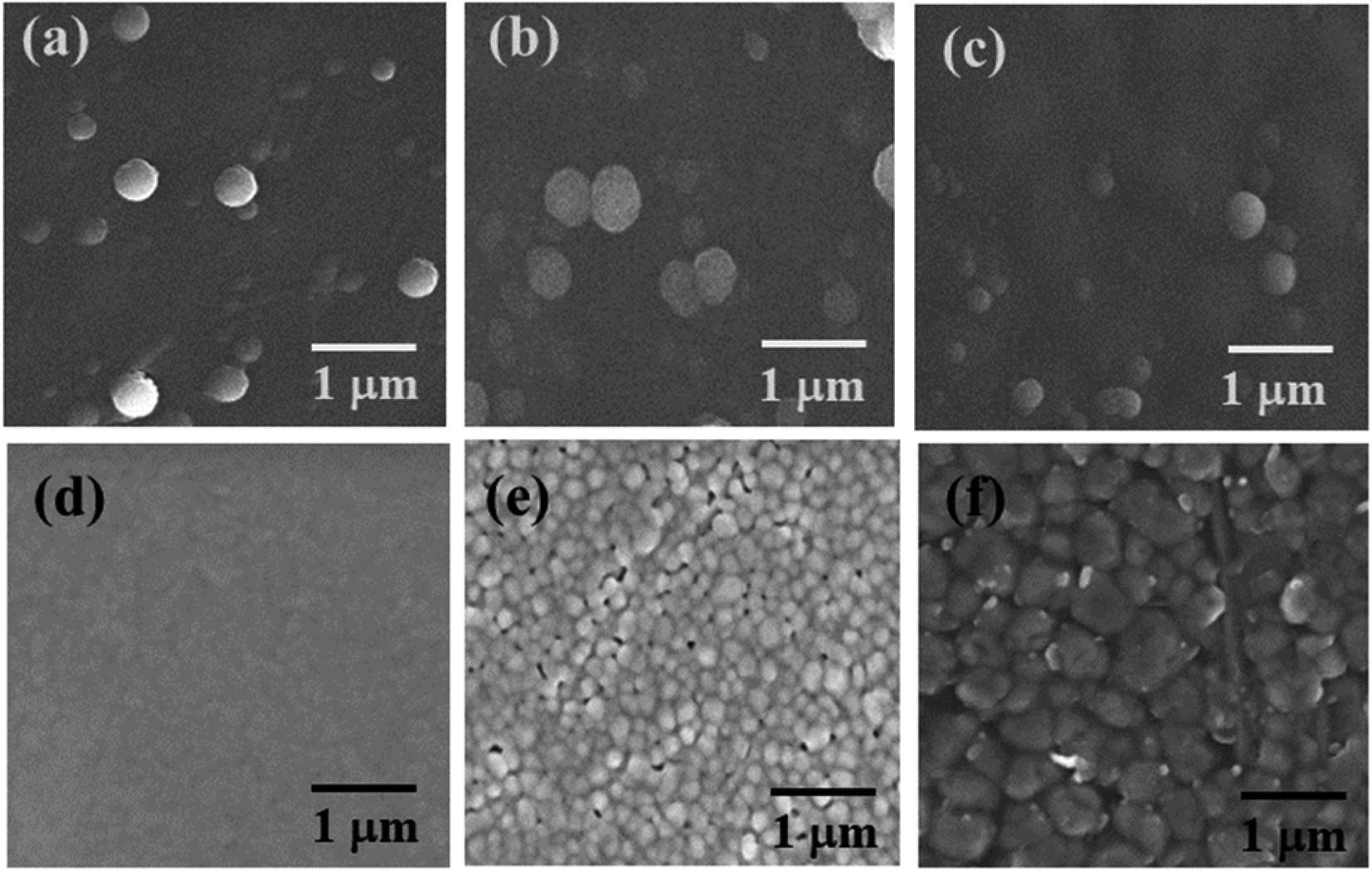 | ||
| Fig. 3 Top view SEM images of (a) pristine TiO2 compact layer (b) Cs-TiO2 compact layer (c) Y-TiO2 compact layer (d) PbI2 layer (e) MAPbI3 layer by spin-coating and (f) Spiro-OMeTAD layer. | ||
 | ||
| Fig. 4 Cross-sectional SEM image of the TiO2 compact layer, perovskite layer and Spiro-OMeTAD layer. | ||
From Fig. 3(a–c); the SEM images are similar, and this is an indication that they particles grow in a similar manner. The dopant metal ions have no much effect on the surface morphology as shown in Fig. 3(b and c) compared with Fig. 3(a), which is the pristine TiO2. The SEM image for all the TiO2 layers had no cluster or agglomeration in the formation of the particle. The SEM image were spherical-like shaped in nature. The segregated nanoparticles were because the annealing temperature above 400 °C was able to initiate crystals which are similar in crystallite size as shown in Fig. 3(a–c).
The first step of the perovskite layer formation involves the deposition of densely packed PbI2 nanoparticles as shown in the SEM image of Fig. 3(d). The absence of pinhole in the deposition of PbI2 layer was as a result high spin speed and time during spin coating. The higher the spin speed and time, the better the surface morphology as seen in Fig. 3(d). The SEM image of the PbI2 layer appeared the same on the pristine, Cs- and Y-doped TiO2. However, the transformation of PbI2 layer to perovskite layer shows a different morphology with few pinholes and larger grain sizes in Fig. 3(e). The SEM image in Fig. 3(d and e) indicates that the grain size increases to almost double after conversion to perovskite layer in the second step of the perovskite deposition. The increase in grain size in this layer is advantageous because it prevents Spiro-OMETAD from diffusing into the ETL. This was also observed in the average crystallite size of the nanoparticles calculated with Scherer eqn (1) using the XRD spectra. However, the average grain size of the converted perovskite absorber layer deposited by spin coating technique was estimated from SEM image, and they are 0.43 ± 0.1, 0.22 ± 0.3, and 0.10 ± 0.1 μm for perovskite absorber layer deposited on Cs-doped TiO2, Y-doped TiO2 and pristine TiO2 respectively. The grain boundaries in the converted MAPbI3 layer increases during drying and thermal annealing of the perovskite layer to remove the remnant solvent. Fig. 3(f) shows the surface morphology of the deposited Spiro-OMeTAD layer with larger pores and grain size. The larger grain size was expected in this layer because the spin speed was reduced during spin coating. In addition, the SEM image of perovskite layer grown by CVD as depicted in Fig. S4† show larger grain size. The estimated average grain size of the perovskite layer grown by CVD is 0.857 ± 0.012 μm. From the SEM image in Fig. 3(e) and S4,† the grain boundaries of the perovskite layer grown by spin-coating method show some pin-holes, while the perovskite layer grown by CVD does not show any pin-holes in the grain boundaries. The absence of pin-holes in the perovskite layer grown by CVD is good as it prevents diffusion of HTL into the perovskite layer during deposition.
Fig. 4 shows the cross-sectional SEM image of the layers of the device from the FTO substrate to the Spiro-OMETAD in a sequential manner. The SEM image did not show interfacial diffusion in the layers of the perovskite solar cell. However, the perovskite layer thickness estimated to be larger than both the ETL and HTL was evident on the cross-sectional view of the three major layers in the solar cell device. The three layers created a well-defined interface in the SEM micrograph in Fig. 4. The cross-sectional SEM image of the perovskite layer grown by spin-coating is consistent with the cross-sectional SEM image of perovskite absorber layer grown by CVD as shown in our previous work.39
The EDX Spectra of the ETM, and the elemental composition confirmed that the dopant is present in the material (Fig. S1 ESI†). The EDX Spectra of the perovskite absorber layer show that the elemental compositions in the deposited materials are present (Fig. S2 ESI†). The absent of the dopant materials in the EDX of the perovskite absorber layer on the pristine, Cs-TiO2 and Y-TiO2 could be due to the small percentage amount of the dopant element in the ETL.
4.4 Optical transmittance and absorption spectra
The optical transmittance of the pristine, Cs- and Y-doped TiO2 deposited on FTO substrate is important prior to the deposition of the perovskite layer. This is to ascertain that reasonable amount of solar light can make the absorber layer (perovskite) to generate maximum photo-generated carriers for the solar performance.Fig. S3,† the optical transmittance spectra for bare FTO substrate (black), pristine TiO2 (red), Cs-doped TiO2 (blue) and Y-doped TiO2 (green) measured in the UV-vis region of the electromagnetic spectrum. The optical transmittance spectra show an oscillating spectrum, due to interaction between the light and the atoms. The transmittance of the Cs-doped TiO2 on FTO substrate is lower compared to the other three (bare FTO, pristine TiO2 and Y-doped TiO2). The results are expected because the ionic radius of Cs dopant is much larger than ionic radius of Y dopant, and this tends to absorb more light. The transmittance for the three samples allowed over 50% light through them into the perovskite layer.
Fig. 5 shows the optical absorbance spectra for the PbI2 before conversion to perovskite layer and MAPbI3 layer after conversion to perovskite layer. The absorbance was measured for PbI2 and MAPbI3 deposited on pristine, Cs-doped and Y-doped TiO2. From the absorbance spectra in Fig. 5(a), PbI2 deposited on the Cs-doped TiO2 showed the highest absorbance, followed by Y-doped TiO2.
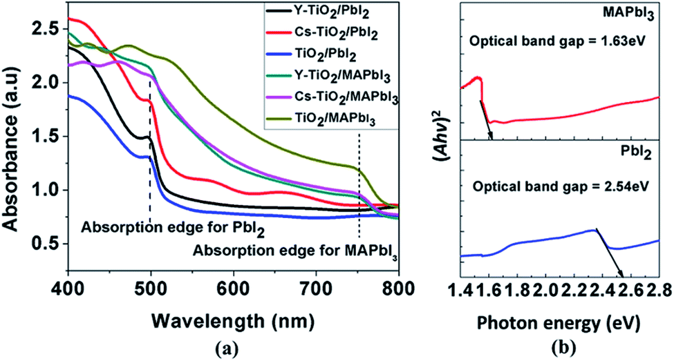 | ||
| Fig. 5 (a) Optical absorbance spectra of the perovskite on pristine, Cs doped and Y doped TiO2 and (b) the corresponding optical band gap of PbI2 and MAPbI3 calculated by Tauc plot. | ||
The absorbance for PbI2 layers deposited on Cs- and Y-doped TiO2 are higher than PbI2 later deposited on pristine TiO2. This observation can be attributed to the larger ionic size of Cs dopant than Y dopant and pristine TiO2. However, the absorption edges in the PbI2 layers absorbance spectra are uniform and occur at 499 nm (2.49 eV). The calculated optical band gap of the PbI2 layer on the three different TiO2 substrates using the Tauc plot is approximately 2.54 eV. The optical band gap was calculated and extrapolated using Kubelka–Munk and Tauc plot for a direct band gap transition as shown in Fig. 5(b). Moreover, the absorption edge was shifted to the wavelength (750 nm) region upon conversion of PbI2 layer to MAPbI3 as shown in the Fig. 5(a). The calculated optical band gap of the converted MAPbI3 layer on the three different TiO2 substrates using Tauc plot is approximately 1.63 eV. The narrowing of the optical band gap of PbI2 layer transformed to MAPbI3 is as a result of structural modification caused by introducing MAI into the system. Both PbI2 and MAPbI3 thin film layers have higher absorption in the visible region of the electromagnetic spectrum.
4.5 J–V characteristics
Fig. 6 and 7 show the best performing solar cells fabricated with different perovskite deposition methods namely: (I) perovskite layer deposited by spin coating as air processed (II) perovskite layer deposited by CVD as vacuum processed. The key parameters η and FF of the perovskite solar cells were calculated using the eqn (2) and (3);41
 | (2) |
 | (3) |
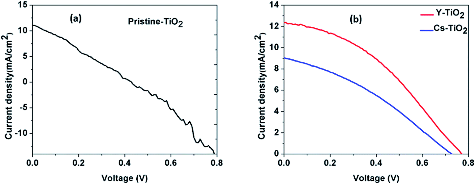 | ||
| Fig. 6 (a) Current density–voltage (J–V) curve for perovskite layer deposited on pristine TiO2 for air processed, (b) current density–voltage (J–V) curve for perovskite layer deposited on Cs-and Y-doped TiO2 for air processed. | ||
| TiO2 layer | JSC (mA cm−2) | VOC (V) | FF | PCE (η) (%) |
|---|---|---|---|---|
| Pristine | 10.71 | 0.44 | 0.31 | 1.45 |
| Cs-doped | 9.05 | 0.73 | 0.34 | 2.21 |
| Y-doped | 12.34 | 0.77 | 0.38 | 3.61 |
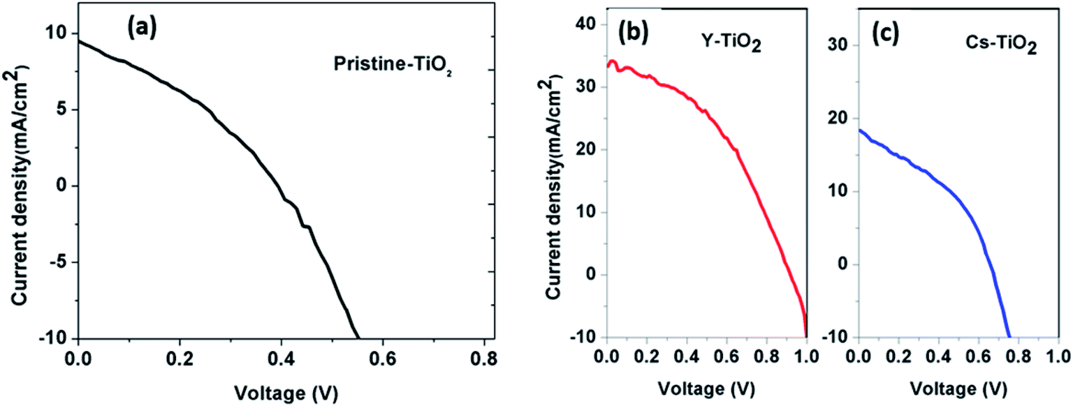 | ||
| Fig. 7 (a) Current density–voltage (J–V) curve for perovskite layer deposited on pristine TiO2 for vacuum processed, current density–voltage (J–V) curve for perovskite layer deposited on (b) Y- doped TiO2 and (c) Cs-doped TiO2 for vacuum processed. | ||
| TiO2 layer | JSC (mA cm−2) | VOC (V) | FF | PCE (η) (%) |
|---|---|---|---|---|
| Pristine | 9.88 | 0.39 | 0.35 | 1.35 |
| Cs-doped | 18.58 | 0.66 | 0.38 | 4.66 |
| Y-doped | 33.71 | 0.85 | 0.45 | 12.89 |
5. Conclusions
In summary, we successfully synthesized three different kinds of titanium precursors for the deposition of electron transporting layers to improve electron extraction from the perovskite active layer. The perovskite layer was deposited using two steps deposition by spin-coating in air and CVD in vacuum. The effect of doping TiO2 and the perovskite layer deposition method on the optical absorption, structural properties, surface morphology and efficiency were studied. The efficiency was enhanced by doping the TiO2 with yttrium which had ionic radius comparable with titanium(IV) ionic radius. However, short-circuit current density for complete devices made from perovskite absorber layer on Y-TiO2 for vacuum processed, show a higher JSC above 25 mA cm−2. For perovskite layers deposited by spin coating and CVD, the efficiencies were calculated to be 3.61% and 12.89% respectively. These results suggest that a perovskite solar cells fabricated in a vacuum produce a high quality stable perovskite solar cell with an enhanced PCE.Conflicts of interest
There are no conflicts to declare.Acknowledgements
The authors acknowledge the financial support from AE-FUNAI TETFUND. C. A. acknowledges the financial support of the National Research Foundation of South Africa. FIE (90407830) graciously acknowledge UNISA for VRSP Fellowship award. We graciously acknowledge the grant by NCC under contract number NCC/R&D/UNN/014.References
- H. S. Kim, C. R. Lee and J. H. Im, et al., Lead iodide perovskite sensitized all-solid-state submicron thin film mesoscopic solar cell with efficiency exceeding 9%, Sci. Rep., 2012, 2, 1–7, DOI:10.1038/srep00591.
- W. S. Yang, B.-W. Park and E. H. Jung, et al., Iodide management in formamidinium-lead-halide-based perovskite layers for efficient solar cells, Science, 2017,(6345), 356, DOI:10.1126/science.aan2301.
- S. G. H. Mohammed and M. G. Tessema, Mixed Halide Perovskite Solar Cells : Progress and Challenges Mixed Halide Perovskite Solar Cells : Progress and Challenges, Crit. Rev. Solid State Mater. Sci., 2019, 1–28, DOI:10.1080/10408436.2018.1549976.
- Q. Wali, N. K. Elumalai, Y. Iqbal, A. Uddin and R. Jose, Tandem perovskite solar cells, Renewable Sustainable Energy Rev., 2018, 84, 89–110, DOI:10.1016/j.rser.2018.01.005.
- H. Kim, K. G. Lim and T. W. Lee, Planar heterojunction organometal halide perovskite solar cells: Roles of interfacial layers, Energy Environ. Sci., 2016, 9, 12–30, 10.1039/c5ee02194d.
- M. Liu, M. B. Johnston and H. J. Snaith, Efficient planar heterojunction perovskite solar cells by vapour deposition, Nature, 2013, 501, 395–398, DOI:10.1038/nature12509.
- Z. H. Bakr, Q. Wali, A. Fakharuddin, L. Schmidt-Mende, T. M. Brown and R. Jose, Advances in hole transport materials engineering for stable and efficient perovskite solar cells, Nano Energy, 2017, 34, 271–305, DOI:10.1016/j.nanoen.2017.02.025.
- Y. Rong, Z. Ku and A. Mei, et al., Hole-conductor-free mesoscopic TiO2/CH3NH3PbI3 heterojunction solar cells based on anatase nanosheets and carbon counter electrodes, J. Phys. Chem. Lett., 2014, 5(12), 2160–2164, DOI:10.1021/jz500833z.
- A. Mei, X. Li and L. Liu, et al., A hole-conductor-free, fully printable mesoscopic perovskite solar cell with high stability, Science, 2014, 345(6194), 295–298, DOI:10.1126/science.1254763.
- M. Wu, S. Chan, M. Jao and W. Su, Solar Energy Materials & Solar Cells Enhanced short-circuit current density of perovskite solar cells using Zn-doped TiO2 as electron transport layer, Sol. Energy Mater. Sol. Cells, 2016, 157, 447–453, DOI:10.1016/j.solmat.2016.07.003.
- Y. Yamada, T. Nakamura, M. Endo, A. Wakamiya and Y. Kanemitsu, Photocarrier recombination dynamics in perovskite CH3NH 3PbI3 for solar cell applications, J. Am. Chem. Soc., 2014, 136(33), 11610–11613, DOI:10.1021/ja506624n.
- N. Marinova, W. Tress and R. Humphry-Baker, et al., Light harvesting and charge recombination in CH3NH3PbI3 perovskite solar cells studied by hole transport layer thickness variation, ACS Nano, 2015, 9(4), 4200–4209, DOI:10.1021/acsnano.5b00447.
- B. N. Ezealigo, A. C. Nwanya and S. Ezugwu, et al., Method to control the optical properties: Band gap energy of mixed halide organolead perovskites, Arabian J. Chem., 2017, 13(1), 988–997, DOI:10.1016/j.arabjc.2017.09.002.
- Q. Chen, H. Zhou and T. B. Song, et al., Controllable self-induced passivation of hybrid lead iodide perovskites toward high performance solar cells, Nano Lett., 2014, 14(7), 4158–4163, DOI:10.1021/nl501838y.
- W. Yin, L. Pan, T. Yang and Y. Liang, Recent advances in interface engineering for planar heterojunction perovskite solar cells, Molecules, 2016, 21(7), 1–19, DOI:10.3390/molecules21070837.
- A. Fakharuddin, L. Schmidt-mende, G. Garcia-belmonte, R. Jose and I. Mora-sero, Interfaces in Perovskite Solar Cells, Adv. Energy Mater., 2017, 1700623, DOI:10.1002/aenm.201700623.
- M. M. Lee, J. Teuscher, T. Miyasaka, T. N. Murakami and H. J. Snaith, Efficient hybrid solar cells based on meso-superstructured organometal halide perovskites, Science, 2012, 338(6107), 643–647, DOI:10.1126/science.1228604.
- D. Y. Son, J. H. Im, H. S. Kim and N. G. Park, 11% efficient perovskite solar cell based on ZnO nanorods: An effective charge collection system, J. Phys. Chem. C, 2014, 118(30), 16567–16573, DOI:10.1021/jp412407j.
- X. Wang, Z. Li and W. Xu, et al., TiO2 nanotube arrays based flexible perovskite solar cells with transparent carbon nanotube electrode, Nano Energy, 2015, 11, 728–735, DOI:10.1016/j.nanoen.2014.11.042.
- T. S. Su, T. Y. Hsieh, C. Y. Hong and T. C. Wei, Electrodeposited Ultrathin TiO2 Blocking Layers for Efficient Perovskite Solar Cells, Sci. Rep., 2015, 5, 16098, DOI:10.1038/srep16098.
- A. Fakharuddin, F. D. Giacomo and A. L. Palma, et al., Vertical TiO2 Nanorods as a Medium for Stable and High-Efficiency Perovskite Solar Modules, ACS Nano, 2015,(8), 8420–8429, DOI:10.1021/acsnano.5b03265.
- T. Zhu and S. P. Gao, The stability, electronic structure, and optical property of TiO2 polymorphs, J. Phys. Chem. C, 2014, 118(21), 11385–11396, DOI:10.1021/jp412462m.
- J. van de Lagemaat, N.-G. Park and A. J. Frank, A study by electrical impedance and optical modulation techniques, J. Phys. Chem. B, 2000, 104(9), 2044–2052, DOI:10.1021/jp993172v.
- F. Azri, A. Meftah, N. Sengouga and A. Meftah, Electron and hole transport layers optimization by numerical simulation of a perovskite solar cell, Sol. Energy, 2019, 181, 372–378, DOI:10.1016/j.solener.2019.02.017.
- A. I. Rafieh, P. Ekanayake, A. Wakamiya, H. Nakajima and C. M. Lim, Enhanced performance of CH3NH3PbI3-based perovskite solar cells by tuning the electrical and structural properties of mesoporous TiO2 layer via Al and Mg doping, Sol. Energy, 2019, 177, 374–381, DOI:10.1016/j.solener.2018.11.024.
- X. X. Gao, Q. Q. Ge and D. J. Xue, et al., Tuning the Fermi-level of TiO2 mesoporous layer by lanthanum doping towards efficient perovskite solar cells, Nanoscale, 2016, 8, 16881–16885, 10.1039/c6nr05917a.
- F. Giordano, A. Abate and J. P. Correa Baena, et al., Enhanced electronic properties in mesoporous TiO2 via lithium doping for high-efficiency perovskite solar cells, Nat. Commun., 2016, 7, 1–6, DOI:10.1038/ncomms10379.
- D. H. Kim, G. S. Han and W. M. Seong, et al., Niobium Doping Effects on TiO2 Mesoscopic Electron Transport Layer-Based Perovskite Solar Cells, ChemSusChem, 2015, 8(14), 2392–2398, DOI:10.1002/cssc.201403478.
- Q. Wali, F. Jan, M. Ejaz, A. Ullah, Y. Iqbal and R. Jose, Advances in stability of perovskite solar cells, Org. Electron., 2020, 78, 105590, DOI:10.1016/j.orgel.2019.105590.
- B. Parida, A. Singh, M. Oh, M. Jeon, J. W. Kang and H. Kim, Effect of compact TiO2 layer on structural, optical, and performance characteristics of mesoporous perovskite solar cells, Mater. Today Commun., 2019, 18, 176–183, DOI:10.1016/j.mtcomm.2018.12.007.
- C. Y. Wu, Y. L. Lee, Y. S. Lo, C. J. Lin and C. H. Wu, Thickness-dependent photocatalytic performance of nanocrystalline TiO2 thin films prepared by sol-gel spin coating, Appl. Surf. Sci., 2013, 280, 737–744, DOI:10.1016/j.apsusc.2013.05.053.
- C. Zhang, Y. Luo and X. Chen, et al., Influence of different TiO2 blocking films on the photovoltaic performance of perovskite solar cells, Appl. Surf. Sci., 2016, 388, 82–88, DOI:10.1016/j.apsusc.2016.03.093.
- R. Songtanasit, T. Taychatanapat and S. Chatraphorn, Electrical Properties of Ultra-thin TiO2 Compact Layer on FTO for Perovskite Solar cells, J. Phys.: Conf. Ser., 2017, 901(1), 012161, DOI:10.1088/1742-6596/901/1/012161.
- M. Morozova, P. Kluson, J. Krysa, M. Vesely, P. Dzik and O. Solcova, Electrochemical properties of TiO2 electrode prepared by various methods, Procedia Eng., 2012, 42, 573–580, DOI:10.1016/j.proeng.2012.07.450.
- S. Das, G. Gu and P. C. Joshi, et al., Low thermal budget, photonic-cured compact TiO2 layers for high-efficiency perovskite solar cells, J. Mater. Chem. A, 2016, 4, 9685–9690, 10.1039/c6ta02105k.
- N. J. Jeon, J. H. Noh, Y. C. Kim, W. S. Yang, S. Ryu and S. Il Seok, Solvent engineering for high-performance inorganic-organic hybrid perovskite solar cells, Nat. Mater., 2014, 13(9), 897–903, DOI:10.1038/nmat4014.
- W. S. Yang, B. W. Park and E. H. Jung, et al., Iodide management in formamidinium-lead-halide-based perovskite layers for efficient solar cells, Science, 2017, 356(6345), 1376–1379, DOI:10.1126/science.aan2301.
- C. Liang, P. Li and Y. Zhang, et al., Mild solution-processed metal-doped TiO2 compact layers for hysteresis-less and performance-enhanced perovskite solar cells, J. Power Sources, 2017, 372, 235–244, DOI:10.1016/j.jpowsour.2017.10.079.
- S. Ngqoloda, C. J. Arendse and T. F. Muller, et al., Air-stable hybrid perovskite solar cell by sequential vapor deposition in a single reactor, ACS Appl. Energy Mater., 2020 DOI:10.1021/acsaem.9b01925.
- U. Nwankwo, R. Bucher, A. B. C. Ekwealor, S. Khamlich, M. Maaza and F. I. Ezema, Synthesis and characterizations of rutile-TiO2 nanoparticles derived from chitin for potential photocatalytic applications, Vacuum, 2019, 161, 49–54, DOI:10.1016/j.vacuum.2018.12.011.
- M. F. Hossain, S. Naka and H. Okada, Annealing effect of E-beam evaporated TiO2 films and their performance in perovskite solar cells, J. Photochem. Photobiol., A, 2018, 360, 109–116, DOI:10.1016/j.jphotochem.2018.04.025.
- W. Chen, H. Sun and Q. Hu, et al., High Short-Circuit Current Density via Integrating the Perovskite and Ternary Organic Bulk Heterojunction, ACS Energy Lett., 2019, 4(10), 2535–2536, DOI:10.1021/acsenergylett.9b01964.
- O. Ergen, S. M. Gilbert and T. Pham, et al., Graded bandgap perovskite solar cells, Nat. Mater., 2017, 16(5), 522–525, DOI:10.1038/nmat4795.
- D. Yang, R. Yang and K. Wang, et al., with negligible hysteresis using EDTA-complexed, Nat. Commun., 2018, 9, 3239, DOI:10.1038/s41467-018-05760-x.
- L. F. Zhu, Y. Z. Xu and J. J. Shi, et al., Efficient perovskite solar cells via simple interfacial modification toward a mesoporous TiO2 electron transportation layer, RSC Adv., 2016, 6(85), 82282–82288, 10.1039/c6ra16839.
Footnote |
| † Electronic supplementary information (ESI) available. See DOI: 10.1039/d0ra01532f |
| This journal is © The Royal Society of Chemistry 2020 |