
 Open Access Article
 This Open Access Article is licensed under a Creative Commons Attribution-Non Commercial 3.0 Unported Licence
Facile synthesis of a dual-phase CsPbBr3–CsPb2Br5 single crystal and its photoelectric performance
Congjian Lin a,
Lai Liua,
Jinzhuo Xua,
Feier Fanga,
Ke Jianga,
Zexiang Liua,
Ye Wangb,
Fuming Chenc and
Huizhen Yao*a
a,
Lai Liua,
Jinzhuo Xua,
Feier Fanga,
Ke Jianga,
Zexiang Liua,
Ye Wangb,
Fuming Chenc and
Huizhen Yao*a
aSZU-NUS Collaborative Innovation Center for Optoelectronic Science & Technology, International Collaborative Laboratory of 2D Materials for Optoelectronics Science and Technology of Ministry of Education, College of Optoelectronic Engineering, Shenzhen University, Shenzhen 518060, China. E-mail: yaohz@szu.edu.cn
bKey Laboratory of Material Physics of Ministry of Education, School of Physics and Engineering, Zhengzhou University, Zhengzhou 450052, China
cSchool of Physics and Telecommunication Engineering, South China Normal University, Guangzhou 510006, China
First published on 1st June 2020
Abstract
The emerging metal-halide perovskites are promising for next generation optoelectronic devices. Recently, all-inorganic halide perovskites have been developed and show significantly improved stability compared with organic–inorganic hybrid halide perovskites. Here, we report a facile method based on the coffee ring effect of solvents to synthesize dual-phase CsPbBr3–CsPb2Br5 single crystal microsheets for the first time. The prepared dual-phase CsPbBr3–CsPb2Br5 single crystal is composed of a tetragonal crystalline phase of CsPb2Br5 and a monoclinic phase of CsPbBr3 according to X-ray diffraction (XRD) patterns. The sharp XRD peaks indicate the high crystallinity of the as-synthesized dual-phase CsPbBr3–CsPb2Br5 microsheets. CsPbBr3 is mainly distributed on the edge of the microsheets based on photoluminescence (PL) mapping images. Besides, a photodetector based on the dual-phase CsPbBr3–CsPb2Br5 microsheets exhibits good performance with a high on/off photocurrent ratio of 300 and a photoresponsivity of 2.68 mA W−1. The rise and decay times of the CsPbBr3–CsPb2Br5 microsheet photodetector are around 25.3 ms and 29.6 ms, respectively. The experimental results indicate that the dual-phase CsPbBr3–CsPb2Br5 microsheet could be a good candidate for the fabrication of high-performance micro photodetectors compatible with practical applications.
1. Introduction
As a promising class of materials, organic–inorganic hybrid lead halide perovskites have recently emerged for cost-effective manufacturing of solar cells, with a remarkable 23.9% power conversion efficiency achieved in just a few years.1–6 Additionally, such perovskite materials have also been explored for a variety of optoelectronic applications including lasers,7 light-emitting diodes (LEDs),8 photodetectors,9,10 and high-sensitivity X-ray detectors with high performance.11 However, organic–inorganic hybrid perovskites suffer from poor environmental stability when they are exposed to ambient air. Thermal and moisture sensitivities hinder the practical applications of this promising material system and understanding equilibrium behaviours (crystallization and decomposition) of organic–inorganic hybrid perovskites in aqueous solution and at different temperatures is very critical.12–16 Recently, the emergence of all-inorganic metal halide perovskites materials can overcome this drawback. They show remarkable stability and unique optoelectronic properties compared with the organic–inorganic hybrid lead halide perovskites.17,18CsPbBr3 and CsPb2Br5 are two types of all-inorganic perovskite materials. Both of them have emerged as attractive semiconducting materials owing to their unique optoelectronic properties.19–25 CsPbBr3 is a three-dimensional (3D) perovskite and the crystal structure of CsPbBr3 is based on the corner-shared PbBr64− octahedra, as shown in Fig. 1a.26 While for the tetragonal CsPb2Br5, it has a quasi two-dimensional (2D) structure, as shown in Fig. 1b. In the structure of tetragonal CsPb2Br5, one layer of Cs+ ions is sandwiched between two layers of Pb2Br5− layers. The Pb2Br5− layers consist of Pb2+ atoms coordinate with eight Br−, forming an elongated polyhedron, which has a staggered arrangement.27 Owing to its unconventional two-dimensional structure, CsPb2Br5 has been investigated broadly for potential applications in optoelectronics.
 | ||
| Fig. 1 Crystal structures of the inorganic perovskites. (a) CsPbBr3. (b) CsPb2Br5. | ||
In past years, several methods have been used to synthesize CsPb2Br5. Wang et al. reported a fast precipitation synthesis of highly luminescent perovskite-related CsPb2Br5 nanoplatelets.28 Tang and Han et al. reported that CsPb2Br5 microplates were synthesized by a modified solution-based process, which is a hot injection method.20,29 Dursun et al. reported that CsPb2Br5 single crystals were obtained from the well-established antisolvent-vapor crystallization (AVC) technique.27 As an indirect bandgap semiconductor, CsPb2Br5 shows PL inactive.27,30,31 But highly luminescent emission from the CsPb2Br5 material can be easily observed in previous reports, which reveals that it is inevitable to bring in CsPbBr3 nanocrystals by using a solution-based method to synthesis CsPb2Br5. For example, Li et al. reported strong luminescence from CsPb2Br5 nanosheets and ascribed to the co-existing CsPbBr3 nanocrystals.31 Zhang et al. reported the embedded CsPbBr3 nanocrystals were primarily responsible for the observed green PL emission in the CsPb2Br5 microplates.32 In addition, dual-phase perovskites have been used in the practical application of high-performance optoelectronic devices. Tong et al. reported dual-phase all-inorganic perovskite composite CsPbBr3–CsPb2Br5 thin films were prepared as light-harvesting layers and incorporated in a photodetector, showing an excellent stability in air for more than 65 day without encapsulation and excellent optoelectronic performance.33 Zhang et al. reported a dual-phase all-inorganic composite CsPbBr3–CsPb2Br5 was developed and used as the emitting layer in LEDs, which exhibited a maximum luminance of 3853 cd m−2, with current density (CE) of ≈8.98 cd A−1 and external quantum efficiency (EQE) of ≈2.21%, respectively.34
In this work, we report a facile synthesis method based on the coffee ring effect of solvent for the growth of dual-phase CsPbBr3–CsPb2Br5 single crystal microsheets on SiO2/Si substrate for the first time. The prepared dual-phase CsPbBr3–CsPb2Br5 microsheets show high crystallinity. Using micro-region Raman measurement, we can see the center region of the dual-phase microsheets have the intrinsic vibrational modes of CsPb2Br5. Then the PL mapping was measured at room temperature. The dual-phase CsPbBr3–CsPb2Br5 microsheets show an edge-luminescent property and the center of the microsheet is nonluminous. This is consistent with the conclusion that CsPb2Br5 with an indirect band gap of ∼3.1 eV is expected to be nonluminous. The bright green emission comes from the CsPbBr3. Furthermore, a prototypical perovskite photodetector was prepared with a coplanar Au/CsPbBr3–CsPb2Br5/Au configuration. This dual-phase CsPbBr3–CsPb2Br5 microsheet photodetector exhibits a light on/off ratio of 300 and a photoresponsivity of 2.68 mA W−1. The result shows the prepared dual-phase CsPbBr3–CsPb2Br5 microsheets have a potential in application of high-performance optoelectronic devices.
2. Experimental section
2.1 Preparation of dual-phase CsPbBr3–CsPb2Br5 microsheets
All chemicals in the experiment were of the highest purity available and used as received without further purification. Distilled water with a resistivity of 18.0 MΩ cm was used throughout this experiment. Typically, 9.1 mg CsBr was firstly put into a bottle and added 2.8 mL N,N-dimethylformamide (DMF). Then placed the bottle in the ultrasonic cleaner for 20 minutes, to promote the dissolution of CsBr. After the dissolution of CsBr in DMF, 14.6 mg PbBr2 powder was added subsequently and dissolved in the bottle to obtain the perovskite precursors. SiO2/Si substrates were cleaned by an ultrasonic cleaner with acetone, isopropanol and anhydrous ethanol for 10 minutes, respectively. Then the substrates were dried by nitrogen gun before we used them. A semiconductor cooling plate was used to cool down the substrate. All the experimental equipments were placed under the fume hood. A Petri dish was placed on the cooling plate and turned on for 15 minutes under 0 °C. Then the precleaned SiO2/Si substrate was placed on the Petri dish and used a pipette gun to drop 7.5 μL precursors on the substrate. After 20 minutes, moved the Petri dish from the cooling plate and used a small fan to dry the samples. The typical growth time for the dual-phase CsPbBr3–CsPb2Br5 microsheets was 25 minutes. After all the DMF evaporated, the dual-phase CsPbBr3–CsPb2Br5 microsheets were moved into the glove box for annealing under N2 atmosphere. The SiO2/Si substrate with dual-phase CsPbBr3–CsPb2Br5 microsheets was annealed at 100 °C for 15 minutes on a heating plate. Finally, the samples were stored in the glove box until they cooled down to room temperature. The prepared samples were dried and cleaned in ambient for further characterization.2.2 Device fabrication
The dual-phase CsPbBr3–CsPb2Br5 microsheets photodetectors were fabricated to investigate their optoelectronic applications. The substrate with dual-phase CsPbBr3–CsPb2Br5 microsheets was covered with a copper mesh with an aperture diameter of 35 microns. Then Au electrodes were deposited on the samples by thermal evaporation method. After the evaporation chamber was cooled down to room temperature, the samples were kept in the evaporation chamber for 10 hours to decrease the contact resistance and increase the contact adhesion to prevent the Au electrodes from peeling off. Finally, the copper mesh was removed and the dual-phase CsPbBr3–CsPb2Br5 microsheet photodetector was fabricated.2.3 Characterizations
The optical images were captured by Nikon LV-100 microscope. The crystal structure was identified by X-ray diffractometer (Rigaku, Ultima IV) using Cu Kα radiation (λ = 1.5418 Å). To characterize the crystallinity of the samples, the microsheets were transferred to the conductive fluorine-doped tin oxide (FTO) glass substrate by a dry transfer method similar to the previous report.35 Raman and PL mapping images were performed using a WITec alpha 300R system equipped with a CCD detector in a backscattering geometry and a typical acquisition time of 5 ms per pixel in PL mapping. A 532 nm solid-state laser was used for the photoexcitation. The laser beam was focused by a 100× objective lens (0.9 NA) from Carl Zeiss Microscopy GmbH and the lateral resolution was estimated to be ∼700 nm. The Raman spectra were collected by 1800 lines per mm grating and calibrated by 520 cm−1 phonon mode from the silicon. Morphology and element compositions of the samples were characterized by field emission scanning electron microscope (SEM, Hitachi, SU8010 MDTC-EQ-M18-01). The atomic force microscopy (AFM) measurements of thickness and surface roughness were carried out on a Dimension Icon AFM (Bruker Nano, Santa Barbara, CA). To investigate the photoelectric performance of the samples, the CsPb2Br5 microsheets photodetector was investigated by MStarter 200 photoelectric testing system. I–V curves were measured under irradiation of different white-light intensities. Photoresponse was measured under irradiation of 532 nm laser.3. Results and discussion
In this work, high crystallinity all-inorganic dual-phase CsPbBr3–CsPb2Br5 microsheets were synthesized by using the coffee ring effect of solvent. The detailed synthesis process is schematically illustrated in Fig. 2a. The inset of Fig. 2c presents the photograph of the CsPbBr3–CsPb2Br5 microsheets grown on the SiO2/Si substrate. A yellow coffee ring contained the CsPbBr3–CsPb2Br5 microsheets could be observed clearly. The coffee ring was formed after the DMF evaporated.36 When the CsBr–PbBr2 precursor droplet dried, the fluid within the precursor droplet was not static. They moved from the center to the edge of the precursor droplet, which is attributed to that the evaporation rate at the edge is faster than that at the central part of the droplet, as shown in Fig. 2b. To keep the surface energy as low as possible, the droplet would form a flow field from the inside to the outside in order to cover the loss of liquid at the edge, so that the CsBr–PbBr2 molecules would move along with the flow field to the edge. As the droplets evaporated, CsBr–PbBr2 molecules then deposited at the edge. The samples were blown with upward wind to accelerate the evaporation of the CsBr–PbBr2 precursor droplet on the substrate and promote the recrystallization of perovskite crystals at the edges. Finally, the single crystal microsheets were formed on the substrate following the evaporation of the droplet and the deposition of the CsBr–PbBr2 molecules. The formation of dual-phase structure was caused by the incomplete phase transition from CsPbBr3 to CsPb2Br5, which can be explained by the following mechanism:28,31,34,37| CsBr + PbBr2 → CsPbBr3 | (1) |
| CsPbBr3 + PbBr2 → CsPb2Br5 | (2) |
 | ||
| Fig. 2 (a) Schematic diagram of the method based on the coffee ring effect of solvent for the synthesis of the sample. (b) Schematic diagram of the outward flow mechanism during evaporation. The mazarine balls represent the CsBr–PbBr2 molecules. (c) OM image of the prepared samples. Inset is the coffee ring on the SiO2/Si substrate. Scale bar is 50 μm. (d) AFM image and a curve showing the thickness of a single microsheets. Scale bar is 2 μm. (e) and (f) SEM images of the sample. Scale bar is 5 μm and 1 μm, respectively. | ||
Dual-phase CsPbBr3–CsPb2Br5 microsheets with well-defined square shapes were obtained and characterized by optical microscopy (OM), as shown in Fig. 2c. In general, the prepared crystals primarily exhibit square sheet morphology. The different colors arising from different thicknesses of the microsheets depend on the diffraction between the bottom and top surface of the microsheets. The lateral dimension of the as-synthesized dual-phase CsPbBr3–CsPb2Br5 microsheets distributes in a range of 1–15 μm typically.
As the AFM image shown in Fig. 2d, the prepared dual-phase CsPbBr3–CsPb2Br5 microsheets possess a typical thickness of ∼50.2 nm, which is perfectly flat in optical level and also is the evidence of highly crystallized nature of dual-phase CsPbBr3–CsPb2Br5 microsheets. The surface morphology of the as-synthesized dual-phase CsPbBr3–CsPb2Br5 were characterized by SEM. Fig. 2e shows the SEM image of the dual-phase CsPbBr3–CsPb2Br5 microsheets and corresponding enlarged image of single microsheet is shown in Fig. 2f. The dual-phase CsPbBr3–CsPb2Br5 microsheet is fairly flat and exhibits a smooth surface, which is free of apparent grain boundaries.
The prepared microsheets were transferred to the conductive fluorine-doped tin oxide (FTO) substrate by a dry transfer method and then investigated by X-ray diffraction measurement.35 As shown in Fig. 3a, the diffraction peaks at 26.6°, 33.8°, 37.9° and 51.6° are indexed to the FTO substrate (JCPDS No. 46-1088). The diffraction peaks at 11.7°, 23.4°, 35.4° and 47.8° correspond to the (002), (200), (312) and (420) planes of CsPb2Br5 (JCPDS No. 25-0211: a = 0.8483 nm, c = 1.525 nm). The diffraction peaks are indexed to standard tetragonal phase CsPb2Br5. The peaks with lower intensity at 15.2° and 28.7° are from lattice planes of monoclinic phase CsPbBr3 (JCPDS No. 18-364: a = b = 0.5827 nm, c = 0.5891 nm). It is seen that CsPb2Br5 is the main composition of the microsheets. As shown in Fig. 3b (partially enlarged XRD patterns), the peaks located at 30.72° is assigned to (202) plane of monoclinic CsPbBr3 while the peak at 30.36° is the (221) plane of tetragonal CsPb2Br5. No other diffraction peaks are observed, indicating high purity of the samples. The diffraction peaks from dual-phase CsPbBr3–CsPb2Br5 are strong and sharp, indicating that the obtained CsPbBr3–CsPb2Br5 microsheets are highly crystalline. The results indicate that the prepared samples are dual-phase CsPbBr3–CsPb2Br5 microsheets. To further analyze the elemental composition and distribution of the samples, energy-dispersive X-ray spectroscopy (EDS) measurement was carried out. The signals of Cs, Pb and Br are clearly identified from the EDS spectra. The integration of the elemental characteristic peaks give quantified atomic ratios (%) of Cs![[thin space (1/6-em)]](https://www.rsc.org/images/entities/char_2009.gif) :Pb:Br corresponding to 14.84:23.03:62.13, which is close to 2:3:8 and corresponded to a mix stoichiometry of CsPbBr3 and CsPb2Br5. As shown in Fig. 3d–f, the Cs, Pb, and Br elements are distributed uniformly across the whole microsheets and overlay with each other perfectly.
:Pb:Br corresponding to 14.84:23.03:62.13, which is close to 2:3:8 and corresponded to a mix stoichiometry of CsPbBr3 and CsPb2Br5. As shown in Fig. 3d–f, the Cs, Pb, and Br elements are distributed uniformly across the whole microsheets and overlay with each other perfectly.
 | ||
| Fig. 3 (a) XRD patterns of the transferred sample. (b) Partial enlarged image of the XRD patterns in (a). (c) EDS results of the dual-phase CsPbBr3–CsPb2Br5 microsheets. (d) The selected SEM image. Scale bar is 5 μm. (e, f and g) Cs, Pb and Br element mapping images. | ||
The optical properties of the dual-phase CsPbBr3–CsPb2Br5 microsheets were investigated by using PL spectroscopy. Under the irradiation of a 405 nm laser, most of the dual-phase microsheets clearly show an edge-luminescent characteristic, as shown in Fig. 4a. PL mapping has been employed to directly visualize the spatial distribution of emission centers. The PL mapping image of a single microsheet is shown in Fig. 4b. As shown in the inset of Fig. 4a, the edges are decorated with individual nanobumps, and these bumps are the source for the edge emission. The inhomogeneous distribution of PL intensity with an edge-luminescent characteristic is caused by a gradual phase transition from the CsPbBr3 edges to the CsPb2Br5 single crystal.37 Besides, the corresponding average PL spectra are shown in Fig. 4c. The peak of PL spectrum is 523 nm which is consistent with the typical emission of CsPbBr3. The result demonstrates the edge-luminescent property of the microsheets comes from the CsPbBr3.38 Additionally, the main composition of the microsheets is CsPb2Br5 with an indirect band gap of ∼3.1 eV that shows nonluminous property.39 Micro-region Raman measurement can reveal the intrinsic lattice vibrational properties of the dual-phase CsPbBr3–CsPb2Br5 microsheets. We measured the central region of the microsheet. As shown in Fig. 4d, the A1g mode (the peaks located at 50 cm−1 and 133 cm−1), B2g mode (the peak located at 69 cm−1) and B1g mode (the peaks located at 41 cm−1 and 79 cm−1) are characteristics peaks of CsPb2Br5. None of the Eg modes are observed in the measured spectrum due to the sheet morphology.40 The results indicate that the prepared microsheets are accompanied by the CsPbBr3 nanocrystals and these nanocrystals are preferably on the edges.37
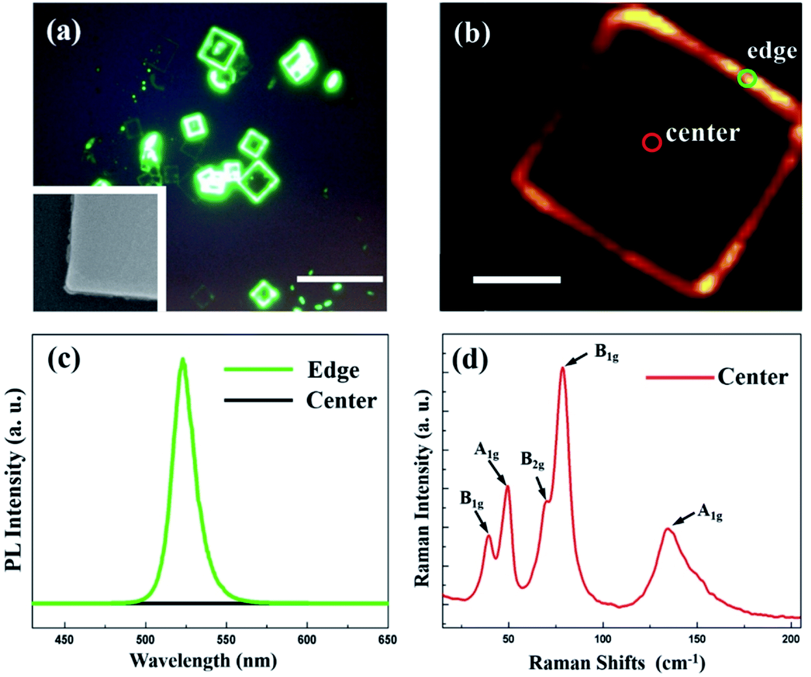 | ||
| Fig. 4 (a) PL microscopic image of the dual-phase CsPbBr3–CsPb2Br5 microsheets. Scale bar is 10 μm. Inset is the high magnification SEM image of an edge-luminescent sample. (b) PL mapping image of a single edge-luminescent dual-phase CsPbBr3–CsPb2Br5 microsheet. Scale bar is 2 μm. (c) PL spectrum of the single microsheet in (b). (d) Raman spectrum of the dual-phase CsPbBr3–CsPb2Br5 microsheets in the center region. | ||
It has been widely reported that the perovskite material serves as a promising candidate for the fabrication of high-performance optoelectronic devices.1–6,9,10,19–25 To demonstrate the application of the dual-phase CsPbBr3–CsPb2Br5 microsheets in a photoelectric device, the photodetector was prepared with a coplanar Au/CsPbBr3–CsPb2Br5/Au configuration. The corresponding schematic diagram is shown in Fig. 5a. Specifically, dual-phase CsPbBr3–CsPb2Br5 microsheets grew on SiO2/Si substrate firstly, and then Au electrode was deposited by thermal evaporation method in vacuum through a shadow mask, the photograph of the device is shown in the inset of Fig. 5a. Fig. 5b shows the energy band diagram of the Au/CsPbBr3–CsPb2Br5/Au structure, in which EC and EV indicate the conduction band minimum and valence band maximum of the dual-phase CsPbBr3–CsPb2Br5, respectively. According to the previous work, CsPbBr3 and CsPb2Br5 have wide band gaps of 2.38 eV and 3.1 eV, respectively, as shown in the inset of Fig. 5b.40,41 Compared to CsPbBr3, CsPb2Br5 contains an abundance of halogens, which accumulate at the interface and connect with the cations to prevent the trapping of the excited electrons by surface defects and reduce the charge carrier recombination. It is helpful to bring in the passivation effect.33 Under illumination, electron–hole pairs are generated within the dual-phase CsPbBr3–CsPb2Br5 microsheet. The tetragonal CsPb2Br5 provides satisfactory passivation to reduce the recombination of the charge carriers. As shown in Fig. 5b, under the applied electric field, electron–hole pairs at the gold–perovskite interface can be separated quickly due to the existence of local electric field in the depletion layer. Thus, the electron–hole recombination rate is effectively reduced and the carrier lifetime increased, which leads to an increase in free carrier concentration. After the photo-generated hole–electron pairs dissociate, electrons in the conduction band will follow to the gold electrode, while the holes in the valence bands will travel to the opposite gold electrode and finally be collected.42–44 Thus, the photocurrent increases gradually as the intensity of light illumination increases. Fig. 5c shows typical I–V curves of the dual-phase CsPbBr3–CsPb2Br5 microsheet photodetector under dark and white-light illumination with various incident light intensities. By changing the incident light power density from dark to 53 mW cm−2, the photocurrent is highly dependent on the light power density. The photocurrent increasing trend attributes to that the amount of photogenerated electron–hole pairs is proportional to the absorbed photon flux. The studied dual-phase CsPbBr3–CsPb2Br5 microsheet photodetector presents a low dark current of 5.94 × 10⁻¹² A under a bias voltage of −4.0 V, and the photocurrent increases by several orders of magnitude to a value of 1.78 × 10⁻⁹ A at the light power density of 53 mW cm−2. Thus, a photocurrent on/off ratio of 300 is achieved.
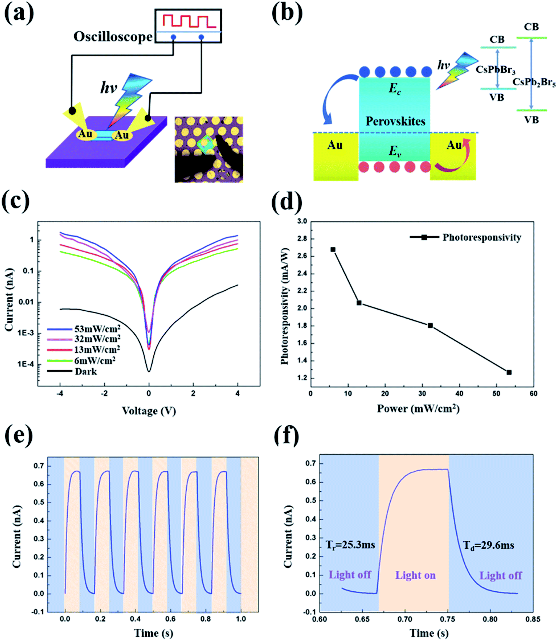 | ||
| Fig. 5 (a) Schematic diagram of the dual-phase CsPbBr3–CsPb2Br5 microsheet photodetector. Inset is the photograph of the device. (b) Energy band alignment of the Au/CsPbBr3–CsPb2Br5/Au structure. Inset is the band gap of CsPbBr3 and CsPb2Br5. (c) I–V curves of the photodetector under dark and different light intensities. (d) Corresponding photoresponsivity of the device under −4 V. (e) Time-dependent photocurrent response of the photodetector under the irradiation of 532 nm laser. (f) Corresponding photocurrent rise and decay curve. | ||
Fig. 5d shows the photoresponsivity of the dual-phase CsPbBr3–CsPb2Br5 microsheet photodetector under a bias voltage of −4 V. The photoresponsivity is defined by the following equation:
 | (3) |
4. Conclusion
In summary, we used a new synthesis method based on the coffee ring effect of solvent to synthesize the micrometer-scale pure phase all-inorganic dual-phase CsPbBr3–CsPb2Br5 microsheets successfully. The XRD, Raman and PL measurements show that the microsheets are hybrid CsPbBr3–CsPb2Br5 with edge of CsPbBr3 and inner of CsPb2Br5. This dual-phase CsPbBr3–CsPb2Br5 preparation method has its own peculiarities compared with the solution-based synthesis method. This work also demonstrates that the micrometer-scale dual-phase CsPbBr3–CsPb2Br5 microsheets are promising in high-performance micro photodetectors, and if they are combined with new 2D materials to form functional heterostructures may lead to high performance optoelectronic applications.Conflicts of interest
There are no conflicts of interest to declare.Acknowledgements
This work was financially supported by the National Natural Science Foundation of China (Grants No. 51602200, 61874074, and 21603192), Educational Commission of Guangdong Province (Grant No. 2016KZDXM008) and the Thousand Young Talents Program of China. This work was partially supported by the Science and Technology Planning Project of Guangdong Province (Grant No. 2016B050501005) the Educational Commission of Guangdong Province (Grant No. 2016KCXTD006), and Shenzhen Peacock Plan (Grant No. KQTD2016053112042971). F. C. thanks the support from Outstanding Young Scholar project (8S0256) from South China Normal University.References
- A. Kojima, K. Teshima, Y. Shirai and T. Miyasaka, J. Am. Chem. Soc., 2009, 131, 6050–6051 CrossRef CAS PubMed.
- S. Bai, Z. Wu, X. Wu, Y. Jin, N. Zhao, Z. Chen, Q. Mei, X. Wang, Z. Ye, T. Song, R. Liu, S. Lee and B. Sun, Nano Res., 2014, 7, 1749–1758 CrossRef CAS.
- H. Zhou, Q. Chen, G. Li, S. Luo, T. Song, H. Duan, Z. Hong, J. You, Y. Liu and Y. Yang, Science, 2014, 345, 542–546 CrossRef CAS PubMed.
- W. Yan, Y. Li, Y. Li, S. Ye, Z. Liu, S. Wang, Z. Bian and C. Huang, Nano Res., 2015, 8, 2474–2480 CrossRef CAS.
- National Renewable Energy Laboratory, Best Research Cell Efficiency, accessed: https://www.nrel.gov/pv/cell-efficiency.html Search PubMed.
- H. Shen, T. Duong, J. Peng, D. Jacobs, N. Wu, J. Gong, Y. Wu, S. K. Karuturi, X. Fu, K. Weber, X. Xiao, T. P. White and K. Catchpole, Energy Environ. Sci., 2018, 11, 394–406 RSC.
- H. Zhu, Y. Fu, F. Meng, X. Wu, Z. Gong, Q. Ding, M. V. Gustafsson, M. T. Trinh, S. Jin and X.-Y. Zhu, Nat. Mater., 2015, 14, 636–642 CrossRef CAS PubMed.
- X. Qin, H. Dong and W. Hu, Sci. China Mater., 2015, 58, 186–191 CrossRef CAS.
- L. Dou, Y. Yang, J. You, Z. Hong, W. Chang, G. Li and Y. Yang, Nat. Commun., 2014, 5, 5404 CrossRef CAS PubMed.
- Y. Fang, Q. Dong, Y. Shao, Y. Yuan and J. Huang, Nat. Photonics, 2015, 9, 679–686 CrossRef CAS.
- H. Wei, Y. Fang, P. Mulligan, W. Chuirazzi, H. Fang, C. Wang, B. Ecker, Y. Gao, M. Loi and L. Cao, Nat. Photonics, 2016, 10, 333–339 CrossRef CAS.
- I. Deretzis, A. Alberti, G. Pellegrino, E. Smecca, F. Giannazzo, N. Sakai, T. Miyasaka and A. La Magna, Appl. Phys. Lett., 2015, 106, 131904 CrossRef.
- J. Yang, B. D. Siempelkamp, D. Liu and T. L. Kelly, ACS Nano, 2015, 9, 1955–1963 CrossRef CAS PubMed.
- M. Ouafi, B. Jaber, L. Atourki, R. Bekkari and L. Laânab, J. Alloys Compd., 2018, 746, 391–398 CrossRef CAS.
- X. Yuan, X. Hou, J. Li, C. Qu, W. Zhang, J. Zhao and H. Li, Phys. Chem. Chem. Phys., 2017, 19, 8934–8940 RSC.
- H. Zhou, Z. Nie, J. Yin, Y. Sun, H. Zhuo, D. Wang, D. Li, J. Dou, X. Zhang and T. Ma, RSC Adv., 2015, 5, 85344–85349 RSC.
- J. Song, L. Xu, J. Li, J. Xue, Y. Dong, X. Li and H. Zeng, Adv. Mater., 2016, 28, 4861–4869 CrossRef CAS PubMed.
- X. Li, Y. Wu, S. Zhang, B. Cai, Y. Gu, J. Song and H. Zeng, Adv. Funct. Mater., 2016, 26, 2435 CrossRef CAS.
- X. Di, L. Shen, J. Jiang, M. He, Y. Cheng, L. Zhou, X. Liang and W. Xiang, J. Alloys Compd., 2017, 729, 526–532 CrossRef CAS.
- C. Han, C. Li, Z. Zang, M. Wang, K. Sun, X. Tang and J. Du, Photon. Res., 2017, 5, 473–480 CrossRef CAS.
- G. Murugadoss, R. Thangamuthu, S. M. Senthil Kumar, N. Anandhan, M. Rajesh Kumar and A. Rathishkumar, J. Alloys Compd., 2019, 787, 17–26 CrossRef CAS.
- M. Shoaib, X. Zhang, X. Wang, H. Zhou, T. Xu, X. Wang, X. Hu, H. Liu, X. Fan, W. Zheng, T. Yang, S. Yang, Q. Zhang, X. Zhu, L. Sun and A. Pan, J. Am. Chem. Soc., 2017, 3, 15592–15595 CrossRef PubMed.
- P. J. Song, B. Qiao, D. D. Song, Z. Q. Liang, D. Gao, J. Y. Cao, Z. H. Shen, X. Zheng and S. L. Zhao, J. Alloys Compd., 2018, 767, 98–105 CrossRef CAS.
- L. Jiang, Z. Fang, H. Lou, C. Lin, Z. Chen, J. Li, H. He and Z. Ye, Phys. Chem. Chem. Phys., 2019, 21, 21996–22001 RSC.
- H. Zhou, L. Fan, G. He, C. Yuan, Y. Wang, S. Shi, N. Sui, B. Chen, Y. Zhang, Q. Yao, J. Zhao, X. Zhang and J. Yin, RSC Adv., 2018, 8, 29089–29095 RSC.
- C. C. Stoumpos, C. D. Malliakas, J. A. Peters, Z. Liu, M. Sebastian, J. Im, T. C. Chasapis, A. C. Wibowo, D. Y. Chung, A. J. Freeman, B. W. Wessels and M. G. Kanatzidis, Cryst. Growth Des., 2013, 13, 2722–2727 CrossRef CAS.
- I. Dursun, M. De Bastiani, B. Turedi, B. Alamer, A. Shkurenko, J. Yin, A. M. El-Zohry, I. Gereige, A. AlSaggaf and O. F. Mohammed, ChemSusChem, 2017, 10, 3746–3749 CrossRef CAS PubMed.
- K. Wang, L. Wu, L. Li, H. Yao, H. Qian and S. Yu, Angew. Chem., 2016, 55, 8328–8332 CrossRef CAS PubMed.
- X. Tang, Z. Hu, W. Yuan, W. Hu, H. Shao, D. Han, J. Zheng, J. Hao, Z. Zang and J. Du, Adv. Opt. Mater., 2017, 5, 1600788 CrossRef.
- B. Qiao, P. Song, J. Cao, S. Zhao, Z. Shen, D. Gao, Z. Liang, Z. Xu, D. Song and X. Xu, Nanotechnology, 2017, 28, 445602 CrossRef PubMed.
- G. Li, H. Wang, Z. Zhu, Y. Chang, T. Zhang, Z. Song and Y. Jiang, Chem. Commun., 2016, 52, 11296–11299 RSC.
- T. Zhang, Z. Chen, Y. Shi and Q. Xu, Nanoscale, 2019, 11, 3186–3192 RSC.
- G. Tong, H. Li, D. Li, Z. Zhu, E. Xu, G. Li, L. Yu, J. Xu and Y. Jiang, Small, 2018, 14, 1702523 CrossRef PubMed.
- X. Zhang, B. Xu, J. Zhang, Y. Gao, Y. Zheng, K. Wang and X. Sun, Adv. Funct. Mater., 2016, 26, 4595–4600 CrossRef CAS.
- C. Huo, X. Liu, X. Song, Z. Wang and H. Zeng, J. Phys. Chem. Lett., 2017, 8, 4785–4792 CrossRef CAS PubMed.
- R. D. Deegan, O. Bakajin, T. F. Dupont, G. Huber, S. R. Nagel and T. A. Witten, Nature, 1997, 389, 827–829 CrossRef CAS.
- C. Wang, Y. Wang, X. Su, V. G. Hadjiev, S. Dai, Z. Qin, S. Chen, Q. Yu, G. Feng, Z. Wang and J. Bao, et al., Adv. Mater., 2019, 31, 1902492 CrossRef PubMed.
- Z. Zhao, B. Ai, C. Liu, Q. Yun, M. Xia, X. Zhao and Y. Jiang, J. Am. Ceram. Soc., 2015, 98, 2117 CrossRef CAS.
- Y. Tan, R. Li, H. Xu, Y. Qin, T. Song and B. Sun, Adv. Funct. Mater., 2019, 29, 1900730 CrossRef.
- V. G. Hadjiev, C. Wang, Y. Wang, X. Su, H. A. Calderon, F. Robles Hernandez, Z. M. Wang and J. M. Bao, Phonon Fingerprints of CsPb2Br5 Single Crystals, J. Phys.: Condens. Matter, 2018, 30, 405703 CrossRef CAS PubMed.
- J. Ramade, L. Andriambariarijaona, V. Steinmetz, N. Goubet, L. Legrand, T. Barisien, F. Bernardot, C. Testelin, E. Lhuillier, A. Bramati and M. Chamarro, Nanoscale, 2018, 10, 6393–6401 RSC.
- Y. Li, Z. Shi, L. Lei, F. Zhang, Z. Ma, D. Wu, T. Xu, Y. Tian, Y. Zhang, G. Du, C. Shan and X. Li, Chem. Mater., 2018, 30, 6744–6755 CrossRef CAS.
- J. Xu, H. Li, S. Fang, K. Jiang, H. Yao, F. Fang, F. Chen, Y. Wang and Y. Shi, J. Mater. Chem. C, 2020, 8, 2102–2108 RSC.
- D. Wu, Y. Jiang, Y. Zhang, Y. Yu, Z. Zhu, X. Lan, F. Li, C. Wu, L. Wang and L. Luo, J. Mater. Chem., 2012, 22, 23272–23276 RSC.
| This journal is © The Royal Society of Chemistry 2020 |