
 Open Access Article
 This Open Access Article is licensed under a Creative Commons Attribution-Non Commercial 3.0 Unported Licence
Ag@BiOCl super-hydrophobic nanostructure for enhancing SERS detection sensitivity†
Huimin Feng‡
 ab,
Fengyou Yang‡a,
Jianjie Donga and
Qian Liu*ab
ab,
Fengyou Yang‡a,
Jianjie Donga and
Qian Liu*ab
aChinese Academy of Sciences (CAS) Key Laboratory of Nanosystem and Hierarchical Fabrication, CAS Center for Excellence in Nanoscience, National Center for Nanoscience and Technology, Beijing 100190, P. R. China. E-mail: liuq@nanoctr.cn
bUniversity of Chinese Academy of Sciences, Beijing 100049, P. R. China
First published on 24th March 2020
Abstract
Surface-enhanced Raman scattering (SERS) has received widespread attention in the rapid detection of trace substances. The super-hydrophobic surface of structures has a significant impact on improving SERS performance. Usually a low concentration of objective molecules is randomly distributed in a large area on a non-hydrophobic SERS substrate, resulting in the Raman signals of the molecules not being easily detected. As a solution, a super-hydrophobic surface can gather a large number of probe molecules around the plasmon hot spots to effectively improve Raman SERS detection sensitivity. In this work, a chloride super-hydrophobic surface is fabricated, for the first time, by a simple and low-cost method of combining surface hydrophobic structures with surface modification. The dispersed and uniform hierarchical Ag@BiOCl nanosheet (Ag@BiOCl NSs) substrate has a higher surface-to-volume ratio and rich nano-gap. Such a chip with a high static contact angle of 157.4° exhibits a Raman signal detection limit of R6G dyes up to 10−9 M and an enhancement factor up to 107. This SERS chip with a super-hydrophobic surface offers great potential in practical applications owing to its simple fabricating process, low cost, large area, and high sensitivity.
Introduction
Surface-enhanced Raman spectroscopy (SERS) as an ultra-sensitive and highly-specific analysis technology can realize low concentration and even single-molecule detection, and has been widely used in medical diagnosis, biosensing, environmental analysis, and food safety.1–5 The SERS effect is mainly caused by (i) the localized surface plasmon resonance (LSPR) generated by metal nanostructures and (ii) chemistry enhancement.6 Numerous studies have been focused on enhancing SERS effect by designing various SERS substrates with metal nanostructures, which can generate some ultra-strong localized electric fields (also known as hot spots) in some special spatial positions.7–10 There is no doubt that generating more hot spots with a stronger electric field on SERS substrate is a dominant strategy to improve SERS detection sensitivity. However, for a real SERS detection of an ultralow-concentration like single-molecule, a fact we have to face is that the molecules free to diffuse into the liquid volume cannot guarantee to fall into a small SERS sensitive area induced by the hot spots, and thus leads to a poor signal-to-noise ratio even a failed SERS detection. One efficient solution is driving a few molecules to hot spots by a super-hydrophobic delivery. In this regard, the super-hydrophobic surface offers great potential, as it can collect high concentration of analyte molecules in a small area by droplet evaporation, making trace substances detection feasible.11SERS structures with super-hydrophobic surface can usually be prepared by chemical and physical methods. For example, F. De Angelis et al. designed and fabricated super-hydrophobic surface with a silicon micro-pillar array by photolithography and electron-beam exposure.11 But its preparation process is time-consuming, expensive and low-yield. By using a chemical synthesis method, various low-cost oxide structures such as Al2O3, ZnO, CuO, and SiO2 can be modified by silver or gold deposited to improve SERS effect,12–17 but the chemical synthesis processes of oxides are complex and the super-hydrophobicity is limited by the metal annealing time. In addition, some biological hierarchical-structure materials in nature also can be used as SERS chips by depositing metal on the natural super-hydrophobic materials.18,19 However, the hierarchical structures are easily destroyed in the dehydration and the depositing process. Therefore, some bionic super-hydrophobic structures are inspired to overcome the dehydration and deposition issues.20
Compared with super-hydrophobic chip with oxide structures, super-hydrophobic chip based on chloride structures is few reported so far. Owing to two dimensions (2D) BiOCl nanosheets (BiOCl NSs) based on bismuth compounds show great potential applications in the field of photocatalysis and photoelectrochemical cells due to their unique layer structure and excellent photostability.21–23 When the BiOCl NSs are irradiated by light, the light is repeatedly reflected in the translucent layer structure, and the formed antibonding state will not weaken the O–Bi–Cl bond force, which makes BiOCl NSs good photostability. Moreover, BiOCl NSs can effectively solve the problem of easy agglomeration of photocatalytic active particles, ensuring a large specific surface area. Therefore, structural properties of BiOCl NSs offer the opportunity to improve surface hydrophobicity and the possibility serving as a multifunctional SERS template.
Generally speaking, artificial super-hydrophobic structures are designable and controllable, but fabrication process is complex and expensive. While common super-hydrophobic surfaces fabricated by chemical syntheses are weaker in SERS performance and reproducibility. In order to solve these issues, combining surface hydrophobic structures with surface modification should be a promising route to fabricate super-hydrophobic substrates.
In this work, we adopt a simple and low-cost method to fabricate large-area hierarchical Ag@BiOCl nanosheets (Ag@BiOCl NSs) super-hydrophobic SERS chip by combining surface structure with surface modification. The SERS chip consists of BiOCl NSs and silver nanoparticles, providing rich surface plasmon hot spots. SERS characterization of such a substrate exhibits a high R6G Raman detectability up to 10−9 M and an enhancement factor up to 107. The finite difference time domain (FDTD) simulation reveals the local electric field intensity distribution of the hierarchical super-hydrophobic structure, further identifying the important role of super-hydrophobic surface in enhancing practical SERS detection sensitivity.
Experimental
Fabrication of Ag@BiOCl NSs
Generally, nanostructures play mainly a role of generating hot spots in a super-hydrophobic surface, and other bigger structures are responsible for the super-hydrophobicity. Thus a super-hydrophobic surface can be simplified to a dual structure. Following this route, we first fabricated BiOCl NSs and then deposited Ag nanoparticles. The detailed processing is shown in Fig. 1. First, amorphous BiOx thin film was deposited on a clean Si substrate by RF reactive magnetron sputtering (Kurt J. Lesker, PVD7) with gas flow ratios Ar (20 sccm) and O2 (5 sccm), respectively. The sputtering power was 50 W and sputtering rate was about 3.3 nm min−1. Second, the sample was soaked in 0.2 M dilute hydrochloric acid solution for 45 seconds to generate the BiOCl NSs.24–26 Then the BiOCl NSs was immersed in alkyl polyglycoside (APG) solution (5 mL of APG and 30 mL of DI) for 10 minutes to modify the surface, and afterwards washed thoroughly with DI water and blew dry with nitrogen. Finally, Ag nanoparticles were deposited on BiOCl NSs at different deposition times (DTs) by magnetron sputtering to generate Ag@BiOCl NSs. | ||
| Fig. 1 Preparation process of Ag@BiOCl NSs structure. | ||
Characterizations
Scanning electron microscopy (SEM, Hitachi SU8220) was used to characterize the surface and cross-section topography of structure. Automatic contact angle measuring instrument (DSA-100) was used to measure the static water contact angle (CA). Raman spectra were collected by Raman spectrometer (Renishaw inVia Plus) in air by a ×100 air objective lens (NA = 0.9) using a 514.5 nm He–Ne laser with a laser spot size of about 1 μm. The integral time was 20 seconds, and laser power at sample position was set 0.5 mW. R6G solution (10 μL) was dropped directly on Ag@BiOCl NSs SERS substrates (dried area around 8.09 mm2) by a pipette and dried in air. All acquired Raman spectra were subtracted from the background baseline.Numerical simulation
The finite-difference time-domain (FDTD) solution was employed to simulate the electric field intensity distribution of the Ag@BiOCl NSs. The incident wave is 514.5 nm at z-direction with incident light polarization angles of 0, 60 and 90 degree, respectively. Perfect matching layers (PML) were applied in z-direction and periodic boundary conditions were applied in x- and y-direction. The mesh sizes were set to 0.25 nm in all directions. The permittivity of Ag was from the Palik's data and the refractive index of 2.15 was chosen for BiOCl.27,28Results and discussion
Characterization and static contact angle (CA) measurements of Ag@BiOCl NSs
In order to study the effect of structure morphology on super-hydrophobicity, we performed SEM characterization and CA measurement of the sample corresponding to each experimental step. Fig. 2(a) shows a homogeneous amorphous BiOx thin film with a thickness of 101.0 ± 1.51 nm, which is deposited on the clean Si substrate. As shown in Fig. 2(b), CA of the BiOx thin film has an increase from 45.4° to 53.4° compared with a clean Si substrate (Fig. S1†). When after the BiOx film is etched for 45 s with diluted HCl solution at room temperature, a large number of uniform ultrathin upright BiOCl NSs with a height of 158.5 ± 8.32 nm are formed at the film surface, as shown in Fig. 2(c). However, CA of BiOCl NSs has a decrease from 53.4° to 49.7°, due to a large number of semi-dangling bonds formed on the surface of BiOCl NSs, as shown in Fig. 2(d), resulting in a hydrophilic in BiOCl NSs surface because these dangling bonds are easily combined with chemical bonds in the water molecule. Here we use the long alkyl chain of the APG solution to functionalize the structure surface, effectively eliminating the effect of the semi-dangling bonds at the structure surface. By comparing the SEM images of BiOCl NSs structure before and after the surface modification shown in Fig. 2(e), the surface modification does not show any change in the structure morphology and no other substances left upon the surface. But CA of BiOCl NSs after surface modification increases dramatically to 148.5°, as shown in Fig. 2(f), which is far higher than that of before surface modification. Although the hydrophobicity obtained by chemical modification may cause unpredictable interference of certain molecules to the Raman signal, the method is the simplest and effective compared to the super-hydrophobic surface obtained only by tuning the specific structure.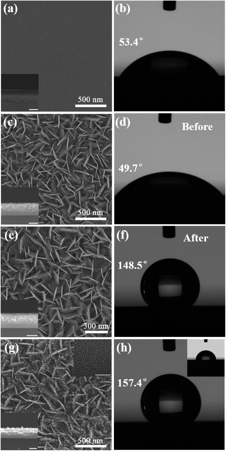 | ||
| Fig. 2 (a and b) SEM image and CA of BiOx thin film. (c and d) SEM image and CA of BiOCl NSs. (e and f) SEM image and CA of BiOCl NSs of surface modification. (g and h) SEM image and CA of Ag@BiOCl NSs. Above inset in (g and h): SEM image after surface modification and CA of Ag nanoparticles on Si substrate after surface modification. Bottom insets in (a), (c), (e), and (g): the corresponding cross-sectional SEM images of different surfaces, respectively. The scale bar is 300 nm. | ||
For increasing hot spots and hydrophobicity, Ag nanoparticles were coated on BiOCl NSs with a deposition time of 70 s to form dual-structure Ag@BiOCl NSs with a thickness of is 162.5 ± 9.31 nm, as shown in Fig. 2(g). Uniform and monodispersed nanoparticles were deposited on BiOCl NSs with a higher surface-to-volume ratio and rich nano-gap. Fig. 2(h) shows that CA of Ag@BiOCl NSs further increases to 157.4°. As shown in the above inset in Fig. 2(g) and (h), SEM images and the corresponding CA of Ag particles on Si substrate is only 78.8°, which is much lower than the CA of the Ag@BiOCl nanosheets after surface modification. Obviously, the Ag nanoparticles on the Si substrate is very limited for enhancing super-hydrophobicity of the chip, but upright BiOCl NSs can effectively increase the super-hydrophobicity of Ag@BiOCl NSs substrate. This is because the air was trapped in the voids at the surface of the BiOCl NSs greatly increasing the air/water interface, which can effectively prevent the penetration of water droplets into the gaps between the Ag@BiOCl NSs and thus result in a good super-hydrophobicity. Therefore, the BiOCl NSs structure plays a dominant role of hydrophobicity in the chip.
The shape and size of BiOCl NSs can affect the super-hydrophobicity of SERS chip, and the gap between adjacent Ag nanoparticles also significantly affects the SERS signal intensity. Fig. 3(a) and (b) display the detailed SEM images of BiOCl NSs after surface modification and Ag@BiOCl NSs. We performed a statistic analysis on the size and distribution features of Ag nanoparticles in BiOCl NSs obtained under a DT of 70 s. The average length and thickness of vertical BiOCl NSs are approximately 192.6 ± 27.5 nm and 9.3 ± 1.45 nm, as shown in Fig. 3(c) and (d). As illustrated in Fig. 3(e) and (f), Ag particles are uniform in size and densely distributed on both sides of the BiOCl NSs. The average size and distance between adjacent Ag particles on the single side of BiOCl NSs are around 22.7 ± 3.65 nm and 3.7 ± 0.70 nm. The size and distance between adjacent Ag particles can be easily and efficiently adjusted by different Ag DTs (Fig. S2†). The distance between adjacent particles was suitable for R6G molecules with the length around 1.3 nm to fit inside, which might contribute to the SERS enhancement.29 Therefore, size-tunable Ag nanoparticles in Ag@BiOCl NSs have an important influence on increasing surface plasmon hot spots.
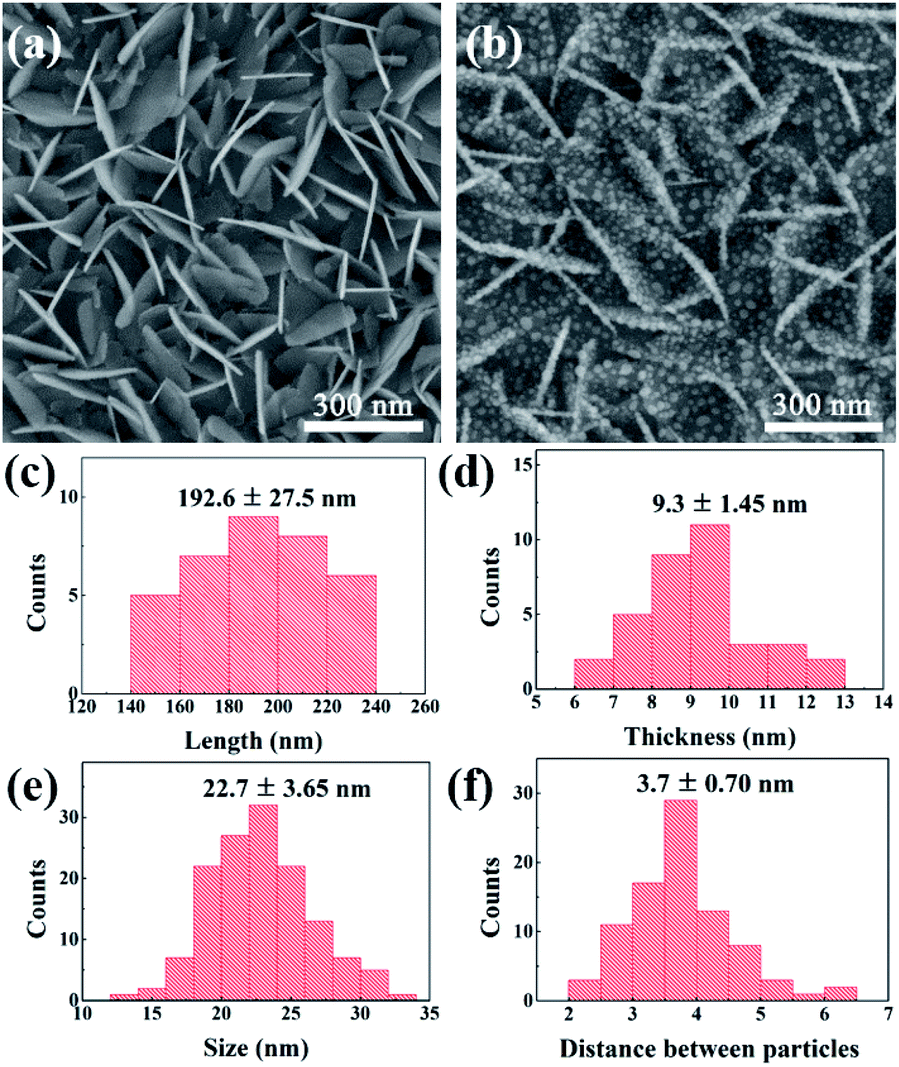 | ||
| Fig. 3 (a) SEM image of BiOCl NSs with super-hydrophobic surface. (b) SEM image of Ag@BiOCl NSs with super-hydrophobic surface. Statistics of (c) length and (d) thickness distribution of BiOCl NSs. Statistics of (e) size and (f) distance between particles distribution of Ag nanoparticles on BiOCl NSs. | ||
Performance of the Ag@BiOCl NSs as SERS chip
In the experiment, Rhodamine 6G (R6G), a common Raman dye, was used as a Raman probe. In order to exclude the effect of other molecules, which may exist in BiOCl NSs surface due to chemical modification, we first performed Raman measurement for the surface-modified BiOCl NSs. As shown in Fig. S3,† by comparing Raman spectra of the surface-modified BiOCl NSs and clean Si substrate, no residual molecule is obviously observed on the BiOCl surface.After that Ag nanoparticles were deposited on the entire surface-modified BiOCl NSs with DT of 30 s, 70 s, and 150 s, respectively. The morphology and distribution of Ag particles on the BiOCl NSs are not uniform for too short (DTs = 30 s) or too long (DTs = 150 s) sputtering time, thus has a negative effect on the intensity of the Raman signal. Raman signal intensities of different Ag@BiOCl NSs were investigated, as shown in Fig. S2,† indicting Raman signal of the chip with DTs of 70 s was stronger than other ones. Considering the super-hydrophobicity and Raman performance, Ag@BiOCl chip with DTs of 70 s was chosen for SERS detection of low concentration R6G dyes. Raman spectra of R6G molecules with a concentration ranging from 10−6 M to 10−9 M were successively obtained, as shown in Fig. 4(a). Fig. 4(b) shows the detailed Raman spectra and intensity of R6G concentrations of 10−8 M and 10−9 M. Raman shift at 1363 cm−1 and 1650 cm−1 are two typical characteristic peaks of R6G molecule. In addition, we also compared to the Raman signal of only Ag film (DT of 70 s) on a Si substrate. The result shows that Raman intensity of Ag@BiOCl NSs with super-hydrophobic surface is far larger than of Ag film on Si substrate at the same concentration (10−7 M) of R6G, as shown in Fig. S4.† This is ascribed to that for the super-hydrophobic surface, gathering more analyte molecules in a smaller area than a hydrophilic surface for the same drop. This means that for a same laser spot, more molecules can be detected on super-hydrophobic surfaces. On the other hand, as shown in Fig. 2(g), Ag nanoparticles that were deposited on the three-dimensional (3D) structure of BiOCl NSs have a higher density per unit area and smaller the spacing between particles, which is beneficial to generating more plasma hot spots and thus enhances Raman signal sensitivity of probe molecules.
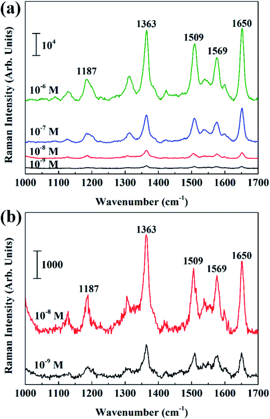 | ||
| Fig. 4 (a) SERS spectra of R6G solution with different concentration (10−6 to 10−9 M) of Ag@BiOCl NSs substrate. (b) The detailed images of Raman spectra at concentrations of 10−8 M and 10−9 M. | ||
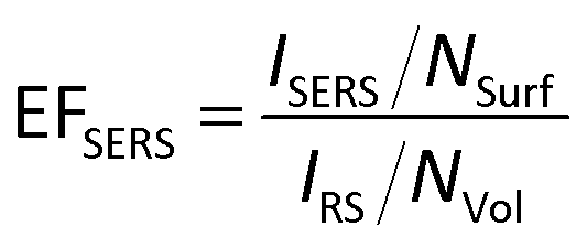
To quantitatively study the SERS enhancement ability of the Ag@BiOCl NSs, the averages EFSERS were estimated according to the conventional expression:30
 | (1) |
To understand the Raman enhancement, we utilized the finite difference time domain (FDTD) method to calculate the electromagnetic field intensity distribution of Ag@BiOCl NSs structures, and further proved such a field enhancement effect. It is well known that the relationship between electromagnetic EF and the normalized electric field (|E|/|E0|) can be approximately by31–33
| EF = [|E|/|E0|]4 | (2) |
In order to obtain an accurate electric field intensity distribution, the topography of Ag@BiOCl NSs can be seen as an alignment of numerous periodic units. We simplify the periodic unit consisting of nanoparticles and BiOCl NSs, as shown in Fig. 5(a). In calculation, the size of Ag particles is set to 22.7 nm. A distance between adjacent Ag particles on the single side of BiOCl NSs is 3.7 nm and thickness of BiOCl NSs is 9.3 nm. According to FDTD simulation, the polarization of the incident plane wave (514.5 nm) is in the x-direction. Fig. 5(b) and (c) demonstrates that the maximum |E|/|E0| value is around 14.7 (red dotted box) from adjacent Ag particles on the single side of BiOCl NSs and is around 12.7 (yellow dotted box) from Ag particles on adjacent BiOCl NSs, respectively. In addition, we simulated the normalized electric field |E|/|E0| at incident light polarization angles of 60 and 90 deg., and the maximum value is more than 19.6 and 14.3, respectively, as shown in Fig. S6.† It can be seen that the maximum normalized electric field is between adjacent Ag particles on the single side of BiOCl NSs for these typical polarization angles of incident light. Therefore, Ag particles distributed densely on BiOCl NSs mainly enhanced the total electromagnetic field. The electromagnetic EF is less than the measured average SERS EFSERS (i.e., 1.25 × 10⁷) because the chemical enhancement is not considered.34 A comparison with Raman detection limit and CA of other hydrophobic SERS substrates is shown in Table S1 (see ESI Section S8†). Since the hierarchical nanostructures cover whole substrate, the significant electromagnetic field enhancement by such a periodic unit dominates the detection of SERS signals, leading to a highly practical sensitivity.
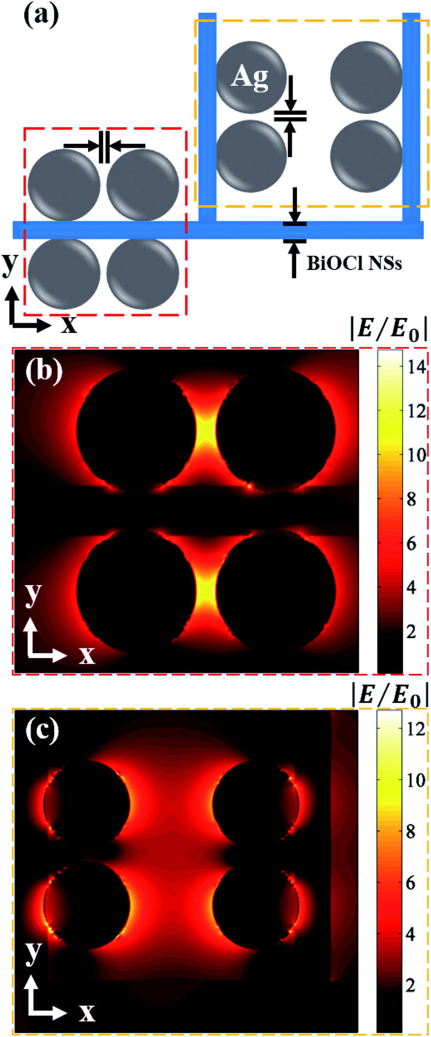 | ||
| Fig. 5 (a) Schematic diagram of periodic unit structure of Ag@BiOCl NSs for calculation. The electric field distribution and normalized electric field intensity (|E|/|E0|) of (b) between adjacent Ag particles on the single side of BiOCl NSs and (c) of Ag particles on adjacent BiOCl NSs. | ||
Conclusions
In summary, we have developed a simple and low-cost way to fabricate large-area super-hydrophobic surface by combining BiOCl NSs structure with chemical modification. This strategy can greatly reduce the dependence of hydrophobicity on the complex nanostructures, and makes the super-hydrophobicity easily available and controlled. The large-area hierarchical Ag@BiOCl NSs SERS chips have a static contact angle up to 157.4° meaning a superior hydrophobicity and corresponding Raman signal detection limit of R6G dyes is up to 10−9 M and enhancement factor is up to 107, which is also confirmed by FDTD simulation. Here super-hydrophobic surface plays an important role because it can collect high concentrations of analyte molecules in a small area, making chip with super-hydrophobic surface easier to detect low concentration of molecules. Consequently, this hierarchical SERS chip with super-hydrophobicity surface offers a promising strategy for further improving SERS performance, and providing many new opportunities in enhancing light-catalysis field.Conflicts of interest
The authors declare no conflict of interest.Acknowledgements
This work was supported by the National Key Research and Development Program of China (2016YFA0200403), the National Natural Science Foundation of China (51971070, 10974037), the CAS Strategy Pilot Program (XDA 09020300), and EU-FP7 Project (No. 247644).Notes and references
- R. A. Tripp, R. A. Dluhy and Y. P. Zhao, Nano Today, 2008, 3, 31–37 CrossRef CAS.
- T. Vo-Dinh, F. Yan and M. B. Wabuyele, J. Raman Spectrosc., 2005, 36, 640–647 CrossRef CAS.
- R. A. Alvarez-Puebla and L. M. Liz-Marzan, Energy Environ. Sci., 2010, 3, 1011–1017 RSC.
- M. Lin, L. He, J. Awika, L. Yang, D. R. Ledoux, H. Li and A. Mustapha, J. Food Sci., 2008, 73, T129–T134 CrossRef CAS PubMed.
- A. J. Haes, L. Chang, W. L. Klein and R. P. Van Duyne, J. Am. Chem. Soc., 2005, 127, 2264–2271 CrossRef CAS PubMed.
- P. L. Stiles, J. A. Dieringer, N. C. Shah and R. P. Van Duyne, Annu. Rev. Anal. Chem., 2008, 1, 601–626 CrossRef CAS PubMed.
- Surface-enhanced Raman Scattering: physics and applications, ed. K. Kneipp, M. Moskovits and H. Kneipp, Springer-Verlag Berlin Heidelberg, Germany, 2006 Search PubMed.
- M. J. Banholzer, J. E. Millstone, L. Qin and C. A. Mirkin, Chem. Soc. Rev., 2008, 37, 885–897 RSC.
- S. Lal, N. K. Grady, J. Kundu, C. S. Levin, J. B. Lassiter and N. J. Halas, Chem. Soc. Rev., 2008, 37, 898–911 RSC.
- Y. Fang, N. H. Seong and D. D. Dlott, Science, 2008, 321, 388–392 CrossRef CAS PubMed.
- F. De Angelis, F. Gentile, F. Mecarini, G. Das, M. Moretti, P. Candeloro, M. L. Coluccio, G. Cojoc, A. Accardo, C. Liberale, R. P. Zaccaria, G. Perozziello, L. Tirinato, A. Toma, G. Cuda, R. Cingolani and E. Di Fabrizio, Nat. Photonics, 2011, 5, 682–687 CrossRef CAS.
- P. Lovera, N. Creedon, H. Alatawi, M. Mitchell, M. Burke, A. J. Quinn and A. O'Riordan, Nanotechnology, 2014, 25, 175502–175507 CrossRef PubMed.
- Y. W. Wu, T. Hang, J. Komadina, H. Q. Ling and M. Li, Nanoscale, 2014, 6, 9720–9726 RSC.
- N. D. Jayrarn, D. Aishwarya, S. Sonia, D. Mangalaraj, P. S. Kumar and G. M. Rao, J. Colloid Interface Sci., 2016, 477, 209–219 CrossRef PubMed.
- A. A. Kowalska, A. Kaminska, W. Adamkiewicz, E. Witkowska and M. Tkacz, J. Raman Spectrosc., 2015, 46, 428–433 CrossRef CAS.
- Z. S. Wang, L. Feng, D. Y. Xiao, N. Li, Y. Li, D. F. Cao, Z. S. Shi, Z. C. Cui and N. Lu, Nanoscale, 2017, 9, 16749–16754 RSC.
- T. Sakano, Y. Tanaka, R. Nishimura, N. N. Nedyalkov, P. A. Atanasov, T. Saiki and M. Obara, J. Phys. D: Appl. Phys., 2008, 41, 235304 CrossRef.
- G. C. Shi, M. L. Wang, Y. Y. Zhu, L. Shen, W. L. Ma, Y. H. Wang and R. F. Li, Sci. Rep., 2018, 8, 6916–6926 CrossRef PubMed.
- J. A. Huang, Y. L. Zhang, Y. Zhao, X. L. Zhang, M. L. Sun and W. Zhang, Nanoscale, 2016, 8, 11487–11493 RSC.
- F. Y. Yang, H. R. Zhang, H. M. Feng, J. J. Dong, C. Wang and Q. Liu, Photonics Res., 2018, 6, 77–83 CrossRef CAS.
- J. Jiang, L. Z. Zhang, H. Li, W. W. He and J. J. Yin, Nanoscale, 2013, 5, 10573–10581 RSC.
- W. Y. Zhu, Z. Li, Y. Zhou and X. L. Yan, RSC Adv., 2016, 6, 64911–64920 RSC.
- S. K. Poznyak and A. I. Kulak, Electrochim. Acta, 1990, 35, 1941–1947 CrossRef CAS.
- C. F. Guo, S. Cao, J. Zhang, H. Tang, S. Guo, Y. Tian and Q. Liu, J. Am. Chem. Soc., 2011, 133, 8211–8215 CrossRef CAS PubMed.
- Y. Tian, C. F. Guo, S. Guo, T. Yu and Q. Liu, Nano Res., 2014, 7, 953–962 CrossRef CAS.
- C. F. Guo, J. Zhang, M. Wang, Y. Tian and Q. Liu, Small, 2013, 9, 2394–2398 CrossRef CAS PubMed.
- E. D. Palik, Handbook of Optical Constants of Solids, Academic Press, San Diego, CA, 1998 Search PubMed.
- X. Q. Zhang, Master Thesis, Sun Yat-Sen University, 2010.
- L. Pérez-Mayen, J. Oliva, A. Torres-Castro and E. De la Rosa, Nanoscale, 2015, 7, 10249–10258 RSC.
- E. C. L. Ru, E. Blackie, M. Meyer and P. G. Etchegoin, J. Phys. Chem. C, 2007, 111, 13794–13803 CrossRef.
- Z. Y. Li, Adv. Opt. Mater., 2018, 6, 1701097 CrossRef.
- H. Xu, J. Aizpurua, M. Käll and P. Apell, Phys. Rev. E: Stat. Phys., Plasmas, Fluids, Relat. Interdiscip. Top., 2000, 62, 4318–4324 CrossRef CAS PubMed.
- C. E. Talley, J. B. Jackson, C. Oubre, N. K. Grady, C. W. Hollars, S. M. Lane, T. R. Huser, P. Nordlander and N. J. Halas, Nano Lett., 2005, 5, 1569–1574 CrossRef CAS PubMed.
- M. Moskovits, Rev. Mod. Phys., 1985, 57, 783–826 CrossRef CAS.
Footnotes |
| † Electronic supplementary information (ESI) available: CA measurements of Si substrate before and after surface modification. Comparison of Raman spectra of surface modified BiOCl NSs, Ag film and Si substrate. SEM images and Raman spectra of Ag@BiOCl NSs with different depositing times. Details about the EF calculations and the FDTD simulation. See DOI: 10.1039/d0ra01226b |
| ‡ These authors contributed equally to the work. |
| This journal is © The Royal Society of Chemistry 2020 |