
 Open Access Article
 This Open Access Article is licensed under a Creative Commons Attribution-Non Commercial 3.0 Unported Licence
Facile synthesis of battery waste-derived graphene for transparent and conductive film application by an electrochemical exfoliation method†
Bagas Prakosoa,
Yuanyuan Mabc,
Ruth Stephanie a,
Naufal Hanif Hawaria,
Veinardi Suendode,
Hermawan Judawisastraa,
Yun Zong*c,
Zhaolin Liu*c and
Afriyanti Sumboja*af
a,
Naufal Hanif Hawaria,
Veinardi Suendode,
Hermawan Judawisastraa,
Yun Zong*c,
Zhaolin Liu*c and
Afriyanti Sumboja*af
aMaterial Science and Engineering Research Group, Faculty of Mechanical and Aerospace Engineering, Institut Teknologi Bandung, Jl. Ganesha 10, Bandung 40132, Indonesia. E-mail: afriyanti.sumboja@material.itb.ac.id
bDepartment of Materials Science and Engineering, National University of Singapore, 117574, Singapore
cInstitute of Materials Research and Engineering (IMRE), A*STAR (Agency for Science, Technology and Research), 2 Fusionopolis Way, Innovis #08-03, 138634, Singapore. E-mail: y-zong@imre.a-star.edu.sg; zl-liu@imre.a-star.edu.sg
dInorganic and Physical Chemistry Research Group, Faculty Mathematics and Natural Sciences, Institut Teknologi Bandung, Jl. Ganesha 10, Bandung 40132, Indonesia
eResearch Center for Nanosciences and Nanotechnology, Institut Teknologi Bandung, Jl. Ganesha 10, Bandung 40132, Indonesia
fNational Centre for Sustainable Transportation Technology (NCSTT), Jl. Ganesha 10, Bandung 40132, Indonesia
First published on 10th March 2020
Abstract
One of the emerging challenges in tackling environmental issues is to treat electronic waste, with fast-growing battery waste as a notable threat to the environment. Proper recycling processes, particularly the conversion of waste to useful & value-added materials, are of great importance but not readily available. In this work, we report a facile and fast production of graphene from graphite extracted from spent Zn–C batteries. The graphene flakes are produced by electrochemically exfoliating graphite under varying DC voltages in poly(sodium 4-styrenesulfonate) (PSS) solution of different concentrations. The exfoliation takes place via the insertion of PSS into the interlayers of graphite to form C–S bonds as confirmed by FTIR and XPS studies. Under an applied voltage of 5 V and in 0.5 M PSS, high quality graphene flakes are obtained in a good yield, giving an ID/IG ratio of about 0.86 in Raman spectroscopy. The transparent conductive film prepared from the dispersion of high quality graphene flakes shows great promise due to its low sheet resistance (Rs) of 1.1 kΩ sq−1 and high transmittance of 89%. This work illustrates an effective and low-cost method to realize large scale production of graphene from electronic waste.
Introduction
In 2014, the International Renewable Energy Agency (IRENA) forecasted that the annual revenue for the battery market will grow by about 80 times over a span of 10 years and reach USD 18 billion in 2023.1 Among the batteries, low-priced Zn–C cells are the most used in portable, low-power electronic devices and are produced in huge volume. Consequently, spent Zn–C batteries are currently a major electronic waste (e-waste) from households, especially in developing countries.2,3 The introduction of the 3R (reduce, reuse, and recycle) strategy does help mitigate the impact of electronic waste to some extent. However, the recycling work so far is fairly preliminary and focusing mainly on the recovery of metals,4 with little done to recycle the graphite which may be readily used for the production of a high-performance, value-added, two-dimensional material, graphene.5,6In fact, since its discovery in 2004, graphene has attracted various attention because of its remarkable merits, such as its high electrical conductivity, transparency, thermal conductivity, tensile strength and high capacitive performance.7,8 These properties mark graphene's potential to make flexible and transparent conductors used in LCDs,9 touch panels,10 electronic papers,11 flexible displays,12 as well as flexible batteries or supercapacitor devices.13,14 Graphene can be produced by bottom-up approach of chemical vapor deposition using suitable chemical precursors, or via top-down methods from graphite by mechanical exfoliation, chemical exfoliation, liquid-phase exfoliation and electrochemical exfoliation.7,15 The electrochemical exfoliation is gaining popularity in the last decade due to its low instrumentation cost, simple procedure, short duration of synthesis, and the possibility to produce high-quality graphene as well as modifying its properties.16–18 Its success has been demonstrated using costly HOPG (highly oriented pyrolytic graphite) and graphite foil,19 with few attempts on graphite rods taken out of battery wastes.4,6,20 In the attempts by Liu et al.6 and Bandi et al.,4 graphene was prepared by electrochemically exfoliating graphite rods in protonic acids of H2SO4 or H3PO4-based, i.e. harmful and toxic electrolytes, which possessed high defect ratio of 0.95 as measured by Raman spectroscopy.4 Later, Tiwari et al.20 tried to use a more environmentally friendly approach by using sodium dodecyl benzenesulfonate (SDBS) surfactant as the electrolyte. However, the considerably high DC voltages (7.5–9 V) that were used during the electrochemical exfoliation produced the insulating graphene oxide.
On the other hand, the fast-growing and large-volume-need of transparent conductive electrode by touch screens, LCDs, OLEDs and solar cells demands supplement or even replacement for their traditional material, ITO (indium tin oxide), which is brittle and costly in production thus unsuitable for emerging applications requiring flexibility.21 Graphene can be a great choice as the substituent, thanks to its low density, robustness, mechanical flexibility, chemical stability, as well as potentially being produced at low cost.22,23 Compared to ITO, it also has a flatter transmittance spectra in the visible and infrared range, highly desirable for solar cell and display applications.24 Chemical vapour deposition can produce transparent graphene film with relatively low resistance (125–600 Ω sq−1), it is however laborious and cost-ineffective.10,25 Transparent and conducting film prepared using graphene flakes produced via electrochemical exfoliation gave diverse qualities with varying sheet resistance.17,26 Yang et al.17 used graphene produced from pristine graphite foil, and made a graphene film with a sheet resistance of 3.91 kΩ sq−1 with the transmittance of 85%. Blair et al.26 was able to achieve even higher transmittance (>90%) for graphene film starting with pristine graphite foil. Unfortunately, the large sheet resistance (100 kΩ sq−1) excludes its applications in transparent conductive electrodes. It remains a challenge to produce high quality graphene film with satisfactory transmittance, good conductivity, cost-efficient, and preferably from the spent batteries.
In this work, we took graphite rods out of spent Zn–C batteries to produce graphene flakes via an electrochemical exfoliation process, using the environmentally friendly poly(sodium 4-styrenesulfonate) (PSS) as the surfactant in the electrolyte. This not only cuts down the amount of battery waste, but also lowers the production cost of graphene (as compared to those made from expensive HOPG and graphite foils). The use of PSS in the electrolyte leads to the formation of graphene–PSS complex, with a zeta potential favoring high yield graphene production.27,28 By varying the PSS concentration in electrolyte and the applied DC voltage, optimum condition is identified for the high-yield production of high quality graphene. The transparent and conductive film fabricated from such graphene exhibited low sheet resistance (Rs) of 1.1 kΩ sq−1 with the transmittance of 89%, comparable to that of the best performers reported previously where the fabrication was notably more complicated and costly.10,26,29
Experimental
The graphite rods were extracted from spent Zn–C batteries produced by the biggest Zn–C batteries manufacturer in Indonesia. They were washed and rinsed with distilled water to remove the contaminants. Poly(sodium 4-styrenesulfonate) (PSS, Mw ∼ 70.000, Sigma-Aldrich) was dissolved in distilled water and diluted to reach various concentrations (0.001, 0.02, 0.1 and 0.5 M) and used as the electrolyte. Graphite rod extracted from unused Zn–C battery was cleansed in the same way and used as the cathode in the electrochemical exfoliation set up. In brief, about 3 cm of the graphite rods were immersed into the PSS electrolyte, and a constant DC voltage (3, 5 and 8 V) from a power supply (GW-INSTEK GPS-3030D) was applied to the system for over 4 hours at room temperature. The obtained dispersion was then centrifuged at 1000 rpm to remove large agglomerates (mostly unexfoliated graphite) at the bottom of the tubes. On the top part of the tube is a stable dispersion of graphene–PSS, which was decanted and kept for further characterizations. Graphene–PSS thin film was prepared by repeatedly dip-coating a glass substrate in the as-obtained graphene–PSS dispersion for 10 times. The deposition parameters, including the dipping rate, drying time and removal speed were controlled to remain constant for all samples.The optical absorption of the samples was characterized using a UV-Vis spectrophotometer (Hewlett Packard Agilent Technologies 8453 series) with quartz cuvettes. Fourier-transform infrared (FTIR) spectra were recorded on a Fourier-Transform Infrared Spectrophotometer (Prestige 21 Shimadzu). XPS data was collected on a Thermo Scientific VG ES-CALAB 200i-XL spectrometer with monochromatized Al Kα (hλ = 1484.6 eV). Crystal structure of the samples were acquired using X-ray diffractometer (XRD, Bruker D8 Advance with Cu Kα radiation (λ = 1.54060 Å)). Raman spectra of the samples were collected using a dispersive micro-Raman spectrometer SENTERRA from Bruker Optics with laser excitation of 532 nm. The Raman spectrometer was equipped with an Andor iDus DU420A CCD detector. During the measurement, the CCD detector was set into a deep-cool mode at −80 °C. The morphology was studied using transmission electron microscope (TEM, HT7700 Hitachi and H9500 Hitachi) and scanning electron microscope (SEM, HITACHI SU3500). The sheet resistance (Rs) of the transparent graphene film was measured with linear four-point probe (with 0.5 mm distance of each probe tip) connected to a current source (GW-INSTEK GPS-3030D) and a multimeter (SUNMA DT830B amperemeter and MASDA DT830D voltmeter). The transmittance of the graphene film was characterized using the same UV-Vis spectrophotometer mentioned above.
Results and discussion
The proposed mechanism of the electrochemical exfoliation of graphite in PSS solution in this study is given in Fig. 1a. It is essentially an anodic exfoliation process where graphite of battery waste is used as the anode. As electrons were drawn away from the graphite anode by a positive current, positive charges are created to encourage the insertion of polystyrenesulfonate anions into the graphite interlayers to maintain the overall charge neutrality. This increases the interlayer spacing between graphene sheets notably, diminishing the interlayer van der Waals force, causing them to fall apart and become discrete graphene sheets.19 Schematic of the electrochemical set up during the electrochemical exfoliation of graphite is given in Fig. S1.† To achieve good quality graphene in high-yield, graphite rods extracted from battery waste were electrochemically exfoliated in PSS solution of varying concentrations (0.001, 0.02, 0.1 and 0.5 M) at selected applied DC voltages (3, 5 and 8 V) over a period of 4 hours. The as-synthesized graphene–PSS dispersion remained stable even after one month of storage (inset of Fig. 1b). At higher PSS concentrations and higher applied voltages, the darkened graphene–PSS dispersions (dark brownish, ESI Fig. S2†) are the indication of higher graphene concentration. UV-Vis spectrophotometry was utilized as the first-cut to semi-quantitatively confirm the formation of graphene. In this case, the absorbance pattern of the graphene–PSS dispersion samples is compared using that of graphite suspension as the control (Fig. 1c and d). The graphite gives an absorbance pattern of little features due to the electronic compressibility by polarization effect in adjacent graphene layers which suppresses its photoluminescence.30 In sharp contrast, graphene–PSS dispersions exhibit a well-defined peak centered at the wavelength of around 300 nm, a characteristic absorbance peak of graphene arising from the π → π* transition of its aromatic C–C bonds.31 From the UV-vis spectra (Fig. 1c and ESI Fig. S3†), it clearly shows that a DC voltage of 3 V is insufficient to initiate the intercalation and exfoliation process for graphite rods from battery waste to produce graphene dispersions in PSS solution. With a PSS concentration of 0.5 M and at an applied DC voltage of 5 V the absorption peak of graphene becomes prominent, which further grows in intensity and is accompanied by a red-shift as the applied voltage was increased to 8 V (Fig. 1c). The higher voltage likely provides a larger driving force for the intercalation process, facilitating more efficient exfoliation of the graphite rods into graphene sheets.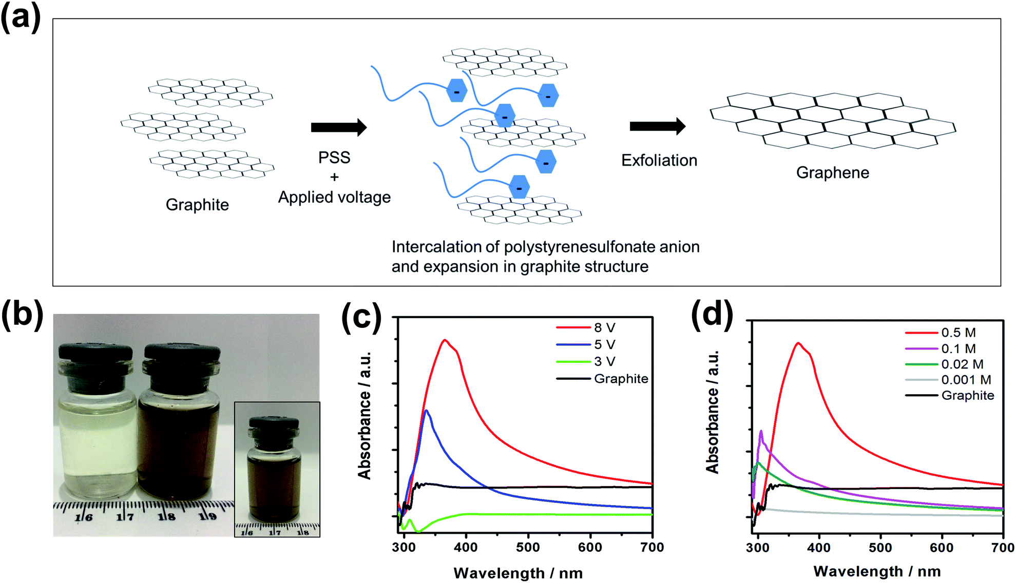 | ||
| Fig. 1 (a) Illustration of graphene synthesis via electrochemical exfoliation in PSS solution. (b) Digital images of 0.5 M PSS solution (left) and graphene–PSS dispersion obtained by electrochemical exfoliation in 0.5 M PSS solution using 8 V of applied DC voltage (right) (inset of a: digital image of the graphene–PSS dispersion, 1 month after synthesis). (c) The UV-Vis spectra of graphene–PSS dispersion obtained via electrochemical exfoliation in 0.5 M PSS solution with varying DC voltages. (d) The UV-Vis spectra of graphene–PSS dispersion obtained via electrochemical exfoliation using 8 V of DC voltage with varying PSS concentrations. UV-Vis spectra of graphite–PSS dispersion is provided in (c) and (d). | ||
At an applied DC voltage of 8 V, but in the electrolytes of lower PSS concentration, the absorption peaks showed notable decrease in the intensity accompanied by a clear blue-shift in the wavelength. The diminishing efficiency at reduced PSS concentration may be due to a lower ionic conductivity of the electrolyte, such that a larger voltage drop takes place in the solution (by larger electrolyte resistance) which resembles the scenarios where a lower applied voltage was adopted. Similar observations were reported previously for graphite of other forms and sources of which electrochemically exfoliated in different electrolytes.32 From the UV-Vis spectra, it can be concluded that the conditions for the most effective electrochemical exfoliation of the battery waste-derived graphite rods in this study is the use of an applied voltage of 8 V at a PSS concentration of 0.5 M. We denote the resultant graphene dispersions as Graphene 0.5/8, and similarly the one is obtained at a voltage of 5 V with the same PSS concentration as Graphene 0.5/5.
The absorption peak red-shift of graphene–PSS dispersion at increased applied voltage and PSS concentration could also be due to the enhanced interactions of graphene sheets with PSS in the dispersion, similar to the report on a graphene–BzCl (benzoyl chloride) dispersion.31 In this study, the graphene and aromatic ring of PSS are responsible for the π–π interaction that leads to the formation of positively charged graphene as most of the electrons in the graphene are attracted by polystyrenesulfonate anion.33,34 Consequently, both the electron–electron and electron–hole interactions in the graphene sheets are screened.35 The higher the charge transfer, the greater the screening effect in the charge carrier of graphene. This explains the longer peak wavelength in the UV absorption spectra of graphene–PSS dispersions at larger applied voltages and higher PSS concentrations.
Raman spectra were recorded from the dispersions of Graphene 0.5/8 and Graphene 0.5/5. Unsurprisingly, two prominent peaks were found in both samples at around 1357 and 1594 cm−1, known as the characteristic D and G peaks of graphene (Fig. 2).36 The former comes from the breathing modes of rings or k-point phonons of A1g symmetry in the graphene structure, while the latter associates with the bond stretching of C sp2 atoms (i.e. E2g phonons).33 The weak peak at 2694 cm−1 is the 2D peak, originating from the second order of zone-boundary phonons in the graphene structure.37 Its much lower intensity here suggests more defects and disorders in the graphene structure, giving more defect-associated bands with a bump-like shaped 2D peak.38
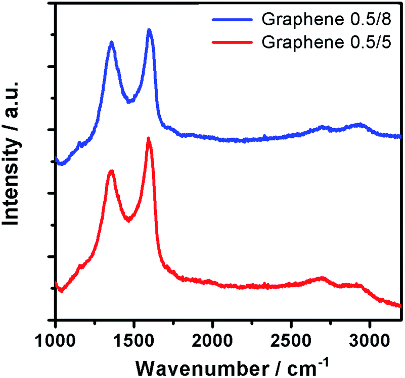 | ||
| Fig. 2 Raman spectra of graphene obtained by electrochemically exfoliating battery waste-derived graphite rods in 0.5 M of PSS concentration at an applied voltage of 8 V (Graphene 0.5/8, blue line) and 5 V (Graphene 0.5/5, red line). Larger ID/IG ratio is seen for Graphene 0.5/8, indicating more defects generated at elevated applied voltage. | ||
The intensity ratio of D and G band (ID/IG) in Raman spectra has been used to determine the quality of graphene, where a higher value elucidates increased defect density in the graphitic structure.39 The ID/IG of Graphene 0.5/8 and Graphene 0.5/5 is about 0.95 and 0.86, respectively, suggesting lower defect density for the latter. This can be understood as with a higher applied voltage in the electrochemical exfoliation process, the intercalation and oxidation reactions were accelerated.40 Similar pattern was observed when we increased the PSS concentration. The high concentration of PSS elevates the ion production which increases the intercalation and exfoliation rate, thereby resulting in more defects in the graphene sheets.41 Hence, Graphene 0.5/5 exhibits higher ID/IG value as compared to Graphene 0.02/5 (ESI Fig. S4†). However, the yield of Graphene 0.02/5 (∼20 mg) is too small for further characterization and practical application. A promising yield about 123 mg can be obtained from Graphene 0.5/5, which is comparable to other reports that utilized similar method.20,42 The ID/IG of Graphene 0.5/5 is higher than that of the graphene obtained from CVD and mechanical exfoliation,10,43 but lower than that of the graphene obtained by electrochemically exfoliating pristine graphite of other sources.29,44
To characterize the functional groups on Graphene 0.5/5, the Fourier-transform infrared (FTIR) spectrum was taken (Fig. 3a). The strong but broad peak at 3050–3800 cm−1 is from the stretching mode of O–H (hydroxyl) group,45 produced over the oxidation reaction in the process of electrochemical exfoliation of graphite. The double peaks at 2918 and 2848 cm−1 come from the symmetric and anti-symmetric stretching modes of CH-group, respectively.46 The one at 2370 cm−1 arises from the anti-symmetric stretching of carbon-oxygen double bond in CO2.47 CO2 was likely the product of a decarboxylation process in the electrochemical exfoliation synthesis of graphene.47 A number of other peaks are around 1381 and 1033 cm−1 for C–O bond, 1714 cm−1 for the vibration of C![[double bond, length as m-dash]](https://www.rsc.org/images/entities/char_e001.gif) O bond,48 1577 cm−1 for CC bond in the graphene structure,47 1174 and 1124 cm−1 for C–S bond.33 The C–S bonds can be formed due to the formation of PSS–graphene complex during the electrochemical exfoliation method. The presence of C–S bond is known to favor higher electrical conductivity,49 thanks to the stronger electron donating sulphur which adds extra electrons as free carriers to increase the charge concentration of graphene.50
O bond,48 1577 cm−1 for CC bond in the graphene structure,47 1174 and 1124 cm−1 for C–S bond.33 The C–S bonds can be formed due to the formation of PSS–graphene complex during the electrochemical exfoliation method. The presence of C–S bond is known to favor higher electrical conductivity,49 thanks to the stronger electron donating sulphur which adds extra electrons as free carriers to increase the charge concentration of graphene.50
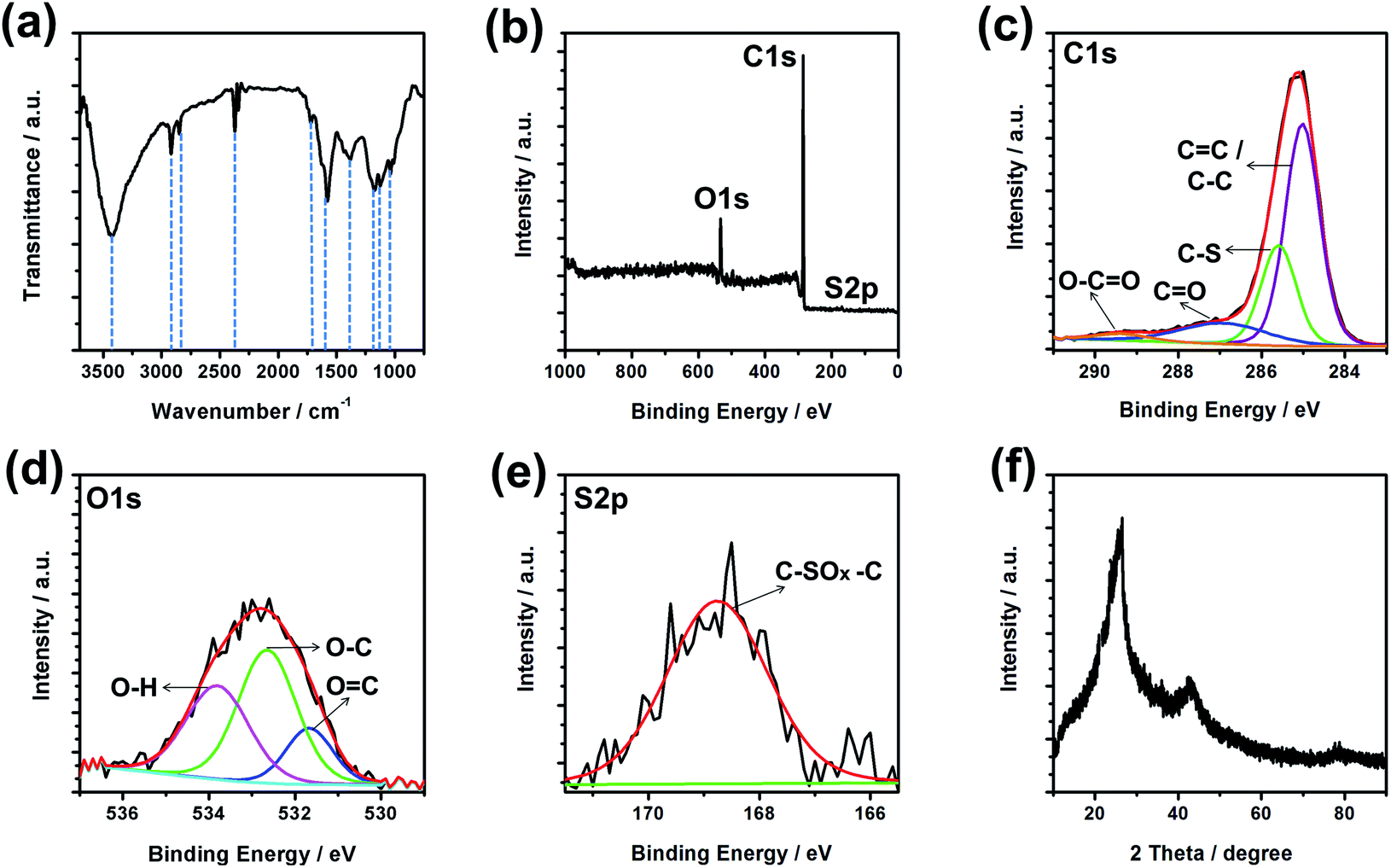 | ||
| Fig. 3 Physical characterizations of Graphene 0.5/5: (a) FTIR spectrum, (b) XPS survey scan, (c) C1s XPS spectra, (d) O1s XPS spectra, (e) S2p XPS spectra and (f) XRD patterns. | ||
The surface elemental composition of Graphene 0.5/5 was probed by X-ray Photoelectron Spectroscopy. The XPS survey scan suggests the presence of C, O, and S, without other noticeable impurities (Fig. 3b). The successful removal of other residues inherited from the Zn–C cells was evidenced by the absence of signals in the Zn2p, Mn2p, Fe2p and Cl2p spectra (ESI Fig. S5†). The C1s spectrum was deconvoluted into four peaks (Fig. 3c) located at 285.02, 285.59, 286.91, and 289.34 eV, for carbon in CC/C–C, C–S, CO, and O–CO, respectively.49,51 The O1s spectrum with a prominent peak can be deconvoluted into three peaks at 531.67, 532.65, and 533.81 eV, for oxygen in carboxyl, epoxy and hydroxyl groups, respectively.52,53 The peak at 168.74 eV for S2p (Fig. 3e) can be associated with C–SOx–C (x = 2, 3, 4),54 further approving the bonding in the PSS–graphene complex as a result of the interactions between polystyrenesulfonate anions and graphene during the electrochemical exfoliation process. The Graphene 0.5/5 was further characterized by X-ray diffractometry and the pattern is shown in Fig. 3f. Two characteristic XRD peaks appear at around 2θ of 26.5° and 44.75°, arising from the diffractions of the (002) and (100) planes in the graphene structure, respectively.55 The interlayer spacing (d-spacing) of graphene calculated from the first peak is about 0.336 nm, similar to those of previous report on graphene.32 The notably smaller value than that of graphene oxide (0.76 nm) which is often rich in hydroxyl, epoxy, carboxyl groups,56 confirms the graphene type structure of Graphene 0.5/5 despite the oxygen element detected in XPS studies. Such structure would promise high electrical conductivity which is beneficial for a wide range of applications. SEM images show that thin graphene sheets with various sizes are stacked together in various orientation (Fig. S6†). The morphology of Graphene 0.5/5 was studied using transmission electron microscope (Fig. 4 and S7†). The nearly transparent feature of these flakes shown in the TEM image suggests that they have a large and transparent lateral dimension (Fig. 4a). The edge of the flakes (Fig. 4b) suggests Graphene 0.5/5 is mainly few-layer or multi-layer graphene. The graphene prepared from electrochemically exfoliating graphite rods in battery waste is used to fabricate transparent and conductive films needed for a number of applications in electronics. Dispersion of Graphene 0.5/5 was fabricated into a thin film by dip-coating method, with that of Graphene 0.5/8 being made in the same way for comparison. The sheet resistance (Rs) of the graphene films were measured using linear four-point probe technique, and shown in Fig. 5a. Notably, both graphene films give relatively decent sheet resistance (1.1 and 1.8 kΩ sq−1), with the Graphene 0.5/5 film also exhibits a high transmittance (89%) at the wavelength of 550 nm (Fig. 5b). The slightly higher sheet resistance of Graphene 0.5/8 film is likely due to its larger fraction of sp3 hybridized carbon (higher ID/IG ratio in Raman spectra) associated with the oxygen functional groups, replacing some of sp2 carbons in graphene which will slow down the electron movement consequently.45 Besides that, the insulating nature of PSS may limit the conductivity of the graphene films.57 Hence, the sheet resistances of these films are on the higher side as compared to CVD graphene (125 Ω sq−1),10 but notably outperform those of the electrochemically exfoliated graphene using starting materials of costly graphite foil or HOPG (2.7–100 kΩ sq−1).17,26,29 Our work presents a facile approach to prepare high quality graphene from battery waste, providing a potential solution to address the e-waste issues with ever-increasing challenges.
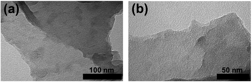 | ||
| Fig. 4 TEM images of Graphene 0.5/5. It is a thin and transparent graphene layer (a), that represents few-layer or multi-layer structure confirmed by its edge (b). | ||
 | ||
| Fig. 5 (a) Sheet resistance and (b) transmittance of a transparent and conductive graphene film prepared from Graphene 0.5/5. Inset of (b): a photo image of the graphene film on a glass substrate. | ||
Conclusion
Facile synthesis of graphene via electrochemically exfoliating graphite rods out of spent Zn–C batteries in PSS solution has been reported. High yield and high-quality graphene is readily obtained under 5 V of DC voltage in 0.5 M PSS, as suggested by the higher absorbance in UV-Vis spectra and lower defect density (i.e. smaller ID/IG ratio) based on the Raman spectra. The higher applied voltage (i.e. 8 V) introduces more defects due to the rapid intercalation and oxidation reactions in the synthesis. In addition, C–S bonds have been detected as a result of the interactions between graphene and PSS in the electrochemical exfoliation process. Transparent and conductive films are readily fabricated using the resultant graphene, showing a low sheet resistance of 1.1 kΩ sq−1 and a high transmittance of 89% at a wavelength of 550 nm. This method not only provides a remedy solution, but also adds economic values to the negative impact of battery waste for the environment.Conflicts of interest
There are no conflicts to declare.Acknowledgements
This work was supported by the Asahi Glass Foundation. This research is partially funded by the Indonesian Ministry of Research, Technology and Higher Education under World Class University (WCU) Program managed by Institut Teknologi Bandung.References
- T. I. R. E. Agency, Battery storage for renewables: market status and technology outlook, 2015 Search PubMed.
- X. Duan, J. Deng, X. Wang, J. Guo and P. Liu, Electrochim. Acta, 2016, 210, 646–654 CrossRef.
- R. Farzana, K. Hassan and V. Sahajwalla, Sci. Rep., 2019, 9, 8982 CrossRef PubMed.
- S. Bandi, S. Ravuri, D. R. Peshwe and A. K. Srivastav, J. Hazard. Mater., 2019, 366, 358–369 CrossRef PubMed.
- J. Deng, X. Wang, X. Duan and P. Liu, ACS Sustainable Chem. Eng., 2015, 3, 1330–1338 CrossRef.
- J. Liu, C. K. Poh, D. Zhan, L. Lai, S. H. Lim, L. Wang, X. Liu, N. G. Sahoo, C. Li and Z. Shen, Nano Energy, 2013, 2, 377–386 CrossRef.
- D. G. Papageorgiou, I. A. Kinloch and R. J. Young, Prog. Mater. Sci., 2017, 90, 75–127 CrossRef.
- G. Chen, T. Chen, K. Hou, W. Ma, M. Tebyetekerwa, Y. Cheng, W. Weng and M. Zhu, Carbon, 2018, 127, 218–227 CrossRef.
- L. Wang, X.-W. Lin, W. Hu, G.-H. Shao, P. Chen, L.-J. Liang, B.-B. Jin, P.-H. Wu, H. Qian and Y.-N. Lu, Light: Sci. Appl., 2015, 4, e253 CrossRef.
- S. Bae, H. Kim, Y. Lee, X. Xu, J.-S. Park, Y. Zheng, J. Balakrishnan, T. Lei, H. R. Kim and Y. I. Song, Nat. Nanotechnol., 2010, 5, 574 CrossRef PubMed.
- W.-L. Song, X.-T. Guan, L.-Z. Fan, W.-Q. Cao, C.-Y. Wang, Q.-L. Zhao and M.-S. Cao, J. Mater. Chem. A, 2015, 3, 2097–2107 RSC.
- J. Lee, T.-H. Han, M.-H. Park, D. Y. Jung, J. Seo, H.-K. Seo, H. Cho, E. Kim, J. Chung and S.-Y. Choi, Nat. Commun., 2016, 7, 1–9 Search PubMed.
- J. Yu, J. Wu, H. Wang, A. Zhou, C. Huang, H. Bai and L. Li, ACS Appl. Mater. Interfaces, 2016, 8, 4724–4729 CrossRef PubMed.
- A. Sumboja, M. Lübke, Y. Wang, T. An, Y. Zong and Z. Liu, Adv. Energy Mater., 2017, 7, 1700927 CrossRef.
- Y. L. Zhong, Z. Tian, G. P. Simon and D. Li, Mater. Today, 2015, 18, 73–78 CrossRef.
- S. Pei, Q. Wei, K. Huang, H.-M. Cheng and W. Ren, Nat. Commun., 2018, 9, 145 CrossRef PubMed.
- S. Yang, S. Brüller, Z.-S. Wu, Z. Liu, K. Parvez, R. Dong, F. Richard, P. Samorì, X. Feng and K. Müllen, J. Am. Chem. Soc., 2015, 137, 13927–13932 CrossRef PubMed.
- Y.-P. Hsieh, W.-Y. Chiang, S.-L. Tsai and M. Hofmann, Phys. Chem. Chem. Phys., 2015, 18, 339–343 RSC.
- P. Yu, S. E. Lowe, G. P. Simon and Y. L. Zhong, Curr. Opin. Colloid Interface Sci., 2015, 20, 329–338 CrossRef.
- S. K. Tiwari, A. Huczko, R. Oraon, A. De Adhikari and G. Nayak, Arabian J. Chem., 2017, 10, 556–565 CrossRef.
- C.-L. Kim, C.-W. Jung, Y.-J. Oh and D.-E. Kim, NPG Asia Mater., 2017, 9, e438 CrossRef.
- X. Hu, L. Chen, T. Ji, Y. Zhang, A. Hu, F. Wu, G. Li and Y. Chen, Adv. Mater. Interfaces, 2015, 2, 1500445 CrossRef.
- T.-H. Han, H. Kim, S.-J. Kwon and T.-W. Lee, Mater. Sci. Eng., R, 2017, 118, 1–43 CrossRef.
- Y. Ma and L. Zhi, Small Methods, 2019, 3, 1800199 CrossRef.
- W. S. Leong, H. Wang, J. Yeo, F. J. Martin-Martinez, A. Zubair, P.-C. Shen, Y. Mao, T. Palacios, M. J. Buehler and J.-Y. Hong, Nat. Commun., 2019, 10, 867 CrossRef PubMed.
- V. E. Blair, K. Celebi, K. Müllen and J. Vermant, Adv. Mater. Interfaces, 2019, 6, 1801570 CrossRef.
- R. J. Smith, M. Lotya and J. N. Coleman, New J. Phys., 2010, 12, 125008 CrossRef.
- J. L. Vickery, A. J. Patil and S. Mann, Adv. Mater., 2009, 21, 2180–2184 CrossRef.
- K. Parvez, R. Worsley, A. Alieva, A. Felten and C. Casiraghi, Carbon, 2019, 149, 213–221 CrossRef.
- M. Hassan, K. R. Reddy, E. Haque, A. I. Minett and V. G. Gomes, J. Colloid Interface Sci., 2013, 410, 43–51 CrossRef.
- W. W. Liu, J. N. Wang and X. X. Wang, Nanoscale, 2012, 4, 425–428 RSC.
- M. Alanyalıoğlu, J. J. Segura, J. Oro-Sole and N. Casan-Pastor, Carbon, 2012, 50, 142–152 CrossRef.
- G. Wang, B. Wang, J. Park, Y. Wang, B. Sun and J. Yao, Carbon, 2009, 47, 3242–3246 CrossRef.
- Y. Y. Wang and P. J. Burke, Nano Res., 2014, 7, 1650–1658 CrossRef.
- L. Yang, Nano Lett., 2011, 11, 3844–3847 CrossRef.
- I. Roy, G. Sarkar, S. Mondal, D. Rana, A. Bhattacharyya, N. R. Saha, A. Adhikari, D. Khastgir, S. Chattopadhyay and D. Chattopadhyay, RSC Adv., 2016, 6, 10557–10564 RSC.
- W. Zhang, Y. Lei, F. Ming, Q. Jiang, P. M. F. J. Costa and H. N. Alshareef, Adv. Energy Mater., 2018, 8, 1801840 CrossRef.
- E. M. Ferreira, M. V. Moutinho, F. Stavale, M. Lucchese, R. B. Capaz, C. Achete and A. Jorio, Phys. Rev. B: Condens. Matter Mater. Phys., 2010, 82, 125429 CrossRef.
- J. Bong, J. H. Park, T. Lim, S. J. Kang, S. K. Kwak and S. Ju, Adv. Mater. Interfaces, 2018, 5, 1800166 CrossRef.
- C.-Y. Yang, C.-L. Wu, Y.-H. Lin, L.-H. Tsai, Y.-C. Chi, J.-H. Chang, C.-I. Wu, H.-K. Tsai, D.-P. Tsai and G.-R. Lin, Opt. Mater. Express, 2013, 3, 1893–1905 CrossRef.
- H. Wang, C. Wei, K. Zhu, Y. Zhang, C. Gong, J. Guo, J. Zhang, L. Yu and J. Zhang, ACS Appl. Mater. Interfaces, 2017, 9, 34456–34466 CrossRef.
- Y. Zhang, Y. Xu, J. Zhu, L. Li, X. Du and X. Sun, Carbon, 2018, 127, 392–403 CrossRef.
- T. S. Tran, S. J. Park, S. S. Yoo, T.-R. Lee and T. Kim, RSC Adv., 2016, 6, 12003–12008 RSC.
- P. Khanra, C.-N. Lee, T. Kuila, N. H. Kim, M. J. Park and J. H. Lee, Nanoscale, 2014, 6, 4864–4873 RSC.
- A. Bagri, C. Mattevi, M. Acik, Y. J. Chabal, M. Chhowalla and V. B. Shenoy, Nat. Chem., 2010, 2, 581 CrossRef CAS.
- N. Parhizkar, B. Ramezanzadeh and T. Shahrabi, Appl. Surf. Sci., 2018, 439, 45–59 CrossRef CAS.
- S. Eigler, C. Dotzer, A. Hirsch, M. Enzelberger and P. Müller, Chem. Mater., 2012, 24, 1276–1282 CrossRef CAS.
- Z. Chen, J. Wang, F. Yu, Z. Zhang and X. Gao, J. Mater. Chem. A, 2015, 3, 11624–11630 RSC.
- A. Sumboja, J. Chen, Y. Ma, Y. Xu, Y. Zong, P. S. Lee and Z. Liu, ChemCatChem, 2019, 11, 1205–1213 CrossRef CAS.
- F. Shahzad, S. Yu, P. Kumar, J.-W. Lee, Y.-H. Kim, S. M. Hong and C. M. Koo, Compos. Struct., 2015, 133, 1267–1275 CrossRef.
- G. Zhou, E. Paek, G. S. Hwang and A. Manthiram, Nat. Commun., 2015, 6, 7760 CrossRef CAS.
- B. Grzyb, S. Gryglewicz, A. Śliwak, N. Diez, J. Machnikowski and G. Gryglewicz, RSC Adv., 2016, 6, 15782–15787 RSC.
- M. A. Marsudi, Y. Ma, B. Prakoso, J. J. Hutani, A. Wibowo, Y. Zong, Z. Liu and A. Sumboja, Catalysts, 2020, 10, 64 CrossRef CAS.
- J. Lee, S. Noh, N. D. Pham and J. H. Shim, Electrochim. Acta, 2019, 313, 1–9 CrossRef CAS.
- Y. Duan, J. Liu, Y. Zhang and T. Wang, RSC Adv., 2016, 6, 73915–73923 RSC.
- S. Natarajan, S. R. Ede, H. C. Bajaj and S. Kundu, Colloids Surf., A, 2018, 543, 98–108 CrossRef CAS.
- Y. Zhou, M. Wang, L. Wang, S. Liu, S. Chen, K. Cao, W. Shang, J. Mai, B. Zhao and J. Feng, Appl. Phys. Lett., 2017, 111, 113302 CrossRef.
Footnote |
| † Electronic supplementary information (ESI) available. See DOI: 10.1039/d0ra01100b |
| This journal is © The Royal Society of Chemistry 2020 |