DOI:
10.1039/D0RA01024C
(Paper)
RSC Adv., 2020,
10, 21860-21866
A bow-free freestanding GaN wafer†
Received
3rd February 2020
, Accepted 18th May 2020
First published on 8th June 2020
Abstract
For applications as high-brightness light-emitting-diodes, a bow-free freestanding gallium nitride (GaN) wafer 2 inch in diameter and ∼185 μm in thickness was fabricated by process-designing pit and mirror GaN layers grown via hydride-vapor-phase epitaxy, laser lift-off, N-face polishing of the pit GaN layer, and three-step polishing of the mirror GaN layer using 3.0 μm-, 0.5 μm-, and 50 nm-diameter diamond abrasives and by inductively-coupled-plasma reactive-ion etching. The considerably large concave shape of the GaN wafer could be decreased by controlling the removal amount of the Ga-face mirror layer during the first step of the polishing process, which approached a bow-free shape or changed with further polishing; this well correlated with the residual stress of the polished GaN wafer.
Introduction
Freestanding gallium nitride (GaN) wafers have been attracting intensive attention for high-grade optoelectronic devices such as high-brightness (HB) ultraviolet and white-light-emitting diodes (LEDs),1–3 field electron emitters,4 and gas sensors5 because of their superior optical6 and electrical7,8 properties. An LED fabricated on a freestanding GaN wafer grown via hydride-vapor-phase epitaxy (HVPE) can improve the quantum efficiency droop in HB-LEDs, i.e., less loss in quantum efficiency at a higher operating current over 200 A cm−2 than a conventional GaN substrate grown via metal organic chemical vapor deposition (MOCVD).9,10 Freestanding GaN wafers have been grown using HVPE,11–13 ammono-thermal,14 and Na-flux15 technologies. HVPE is the most widely used because it enables a fast growth rate (∼100 μm h−1) and large diameter wafer growth (∼6 inch in diameter) in mass production.16 However, for growing a thick GaN layer on a sapphire substrate, it is not easy to fabricate a thick (∼300 μm) and crack-free GaN wafer because the bow is greatly enlarged by the lattice constant and the thermal expansion coefficient (TEC) mismatch between the grown GaN layer and sapphire substrate,17 as shown in Fig. S1.† The lattice constant mismatch between the two materials is as large as ∼13%, which results in a high dislocation density of ∼109 cm−2 in an epitaxially grown GaN layer.18 The TEC mismatch is also as large as ∼25.6%, i.e., the TEC of a sapphire substrate (i.e., 7.5 × 10⁻⁶ K−1) is considerably larger than that of an epitaxially grown GaN layer (i.e., 5.59 × 10⁻⁶ K−1), which leads to biaxial compressive stress in an epitaxial GaN layer when cooling to room temperature from a growth temperature of ∼1000 °C.19 In addition, although the thickness of a GaN layer grown on a sapphire substrate is less than 300 μm to avoid the generation of cracks, the bow of the GaN wafer separated from a sapphire substrate is very high (i.e., −300 μm); hence, several lapping processes are necessary for achieving a bow-free wafer. Note that the GaN wafer is very hard (i.e., the hardness of GaN is ∼11 GPa), due to which it having a thickness of less than 300 μm (i.e., up to ∼100 μm) would show no handling issues during the LED fabrication process. Furthermore, the bow of a freestanding GaN wafer decreases the internal quantum efficiency of HB-LEDs because it increases non-radiative recombination at a high current density operation. In addition, the presence of a GaN wafer bow is a critical issue in the LED fabrication processes, such as in MOCVD GaN growth and photolithography. The bow can cause GaN wafer cracking and peeling-off during the GaN film growth through MOCVD and a misalignment of the LED patterns through lithography.20 Thus, many studies on suppressing the bow in the growth process of an epitaxial GaN layer have been conducted using various technologies, such as the change in the III–V gas ratio for a stress-relaxed GaN layer,21 self-separating GaN from the substrate,22 simultaneous double-side growth of a GaN layer on a sapphire substrate,23 and hydrogen-ion implantation for stress relaxation.24 Even though the GaN wafer bow can be suppressed by the growth techniques, it fluctuates during the wafering process, which makes a prediction of a final GaN wafer bow very difficult.
We therefore investigated the dependency of the GaN wafer bow on the remaining GaN wafer thickness, with regard to the thickness ratio between the pit and mirror GaN layers, to fabricate a bow-free, crack-free, freestanding GaN wafer grown by HVPE. We also examined how the thickness ratio and remaining subsurface damaged layer of a GaN wafer simultaneously affect the fluctuation in GaN wafer bow during the polishing process. Specifically, we designed a three-step polishing process and investigated its effectiveness in suppressing bow and eliminating the surface scratches of a GaN wafer.
Experimental section
GaN layer growth on a sapphire substrate
We conducted an experiment involving a horizontal HVPE reactor to grow a thick GaN layer (i.e., ∼330 μm) on a 2-inch-diameter sapphire substrate. Note that the selection of a sapphire substrate was realistic due to the low wafer price and reasonable crystalline defect density compared to Si (111) and SiC (0001) substrates.25,26 Before GaN growth, we conducted a SC-2(hydrochloric-acid, H2O2, and deionized water mixture solution) cleaning of the sapphire substrates. The HVPE reactor was heated to 800 °C for the source zone and 990 °C for the growth zone in the nitrogen (N2) gas atmosphere. To form gallium chloride gas, hydrochloric acid gas flowed directly into the gallium metal source in N2 gas carrier. After that, ammonia gas directly flowed into the growth zone for the chemical reaction of the epitaxial GaN layer. First, we grew an AlN layer on the sapphire substrate in the horizontal HVPE reactor, with the AlN layer growth done at 990 °C for 5 min under a NH3 gas atmosphere (19![[thin space (1/6-em)]](https://www.rsc.org/images/entities/char_2009.gif) 600 sccm).
600 sccm).
The growth rates for 3-dimensional (3D) (i.e., a pit layer) and 2D growth (i.e., a mirror layer) were determined by the flow rates of HCl and NH3 gases in the GaN growth furnace. The flow rates of HCl and NH3 gases for the pit GaN layer were 1800 and 19600 sccm, respectively, while they were maintained at 1000 and 2000 sccm for the mirror GaN layer. Thus, the 3D and 2D growth rate of our GaN wafers were 1.35 and 0.65 μm min−1.
Then we applied a two-step growth recipe to release thermal stress between the sapphire substrate and the epitaxial GaN layer. For the first step of GaN epitaxial growth, called a pit GaN layer growth, a 100 μm-thick pit GaN layer on a sapphire substrate was grown at a fast growth rate (i.e., ∼100 μm h−1) for stress relaxation, as shown in Fig. S2.† The pit GaN layer growth was done at 990 °C for 75 min under a flow of HCl (1800 sccm) and NH3 (19600 sccm) gases, producing a 2D GaN growth. For the continuous second step of epitaxial GaN layer growth, called a mirror GaN layer growth, a 200 μm-thick GaN mirror layer was grown at a slow growth rate (i.e., ∼50 μm h−1) for achieving a thick and low threading dislocation density of a GaN wafer. The mirror GaN layer growth was done at 990 °C for 300 min under a flow of HCl (1000 sccm) and NH3 (2000 sccm) gases, producing 3D GaN growth. A 330 μm-thick GaN layer was grown on a sapphire substrate, which was convex at room temperature. The surface morphology showed a typical hexagonal hillock grown along 〈10![[1 with combining macron]](https://www.rsc.org/images/entities/char_0031_0304.gif) 0〉 and 〈101〉. The density of hillock and V-shape pits were 16.68 and 75 ea cm−2, as shown in Fig. S3.†
0〉 and 〈101〉. The density of hillock and V-shape pits were 16.68 and 75 ea cm−2, as shown in Fig. S3.†
Separation of the GaN layer from the sapphire substrate
To separate the 330 μm-thick GaN wafer, consisting of a 100 μm-thick pit layer and 230 μm-thick mirror layer, from the sapphire substrate, the laser lift-off (LLO) process was carried out in a furnace at 1100 °C by using a pulse laser system of Nd:YAG 355 nm. After separation, the concavity and thickness of the GaN wafer were −300 and ∼330 μm, respectively. The separated GaN wafer was composed of the 230 μm-thick Ga-face mirror layer vertically stacked on the 100 μm-thick N-face pit layer. Note that LED fabrication was conducted on the Ga-face mirror layer. The bow of the separated GaN wafer after LLO changed from convex to concave. The GaN mirror layer on the GaN pit layer after LLO had a concave wafer bow of −100 to −300 μm.
Fabrication of the GaN wafer
This wafer with a huge bow cannot be polished as it would be easily broken when the wafer is loaded on the head of the polisher. Thus, this wafer with a huge bow was bonded on a ceramic plate by coating a phase change wax on the ceramic plate at 100 °C, then putting on the wafer, with loading a heavy metal weight of ∼30 kg on the wafer at 100 °C, followed by cooling down the ceramic plate to room temperature. Thus, the bonded wafer became flat on the ceramic plate, as shown in Fig. S5(a).† Then, the bonded wafer on the ceramic plate was loaded on the head of the polisher and then the head moved down the table to perform the polishing. A tin resin table was used for the polishing the pit GaN layer. The first polishing of the Ga-face GaN mirror layer was performed using slurry containing ∼3 μm diamond abrasives, while the pure tin table was utilized for the second polishing of the Ga-face GaN mirror layer using ∼0.5 μm diamond abrasives, and the third polishing of the Ga-face GaN mirror layer was performed using ∼50 nm abrasives, as shown in Fig S4(b) and (c).† After polishing, the wafer was deboned from the ceramic plate by heating the ceramic plate so that the wafer returned to the concave bow shape.
Characterization of the GaN wafer
The GaN wafer bow was measured by a digital micrometer (Mitutoyo ID-CX series with the comparator stands (BS series)). The sign of a wafer bow determines the shape of the mirror GaN layer, i.e., (+) bow for convex shape and (−) bow for concave shape. To estimate the wafer bow, first, the height of the wafer center was measured by putting the convex shape wafer on a reference table. Then, the wafer was flipped 180° and loaded on a reference table; afterward, the wafer center thickness was measured. The difference between the height of the convex shape wafer and the center wafer thickness flipped 180° indicated the wafer bow. In addition, the subsurface damaged layer (SSD) of the Ga-face mirror layer after polishing and the morphology of the CMP abrasives were observed by cross-sectional (x-) transmission electron microscopy (TEM) (JEOL JEL-2100F) at an accelerating voltage of 200 keV. The remaining threading dislocations and subsurface-damage-induced scratches were observed by scanning electron microscopy (SEM) (HITACHI S-4300) with cathodoluminescence (CL) (GATAN MONO CL3+). The images of the remaining scratches and surface roughness were estimated by atomic force microscopy (AFM) (Park Systems XE7).
Results and discussion
Bow of the GaN wafer grown on the sapphire substrate
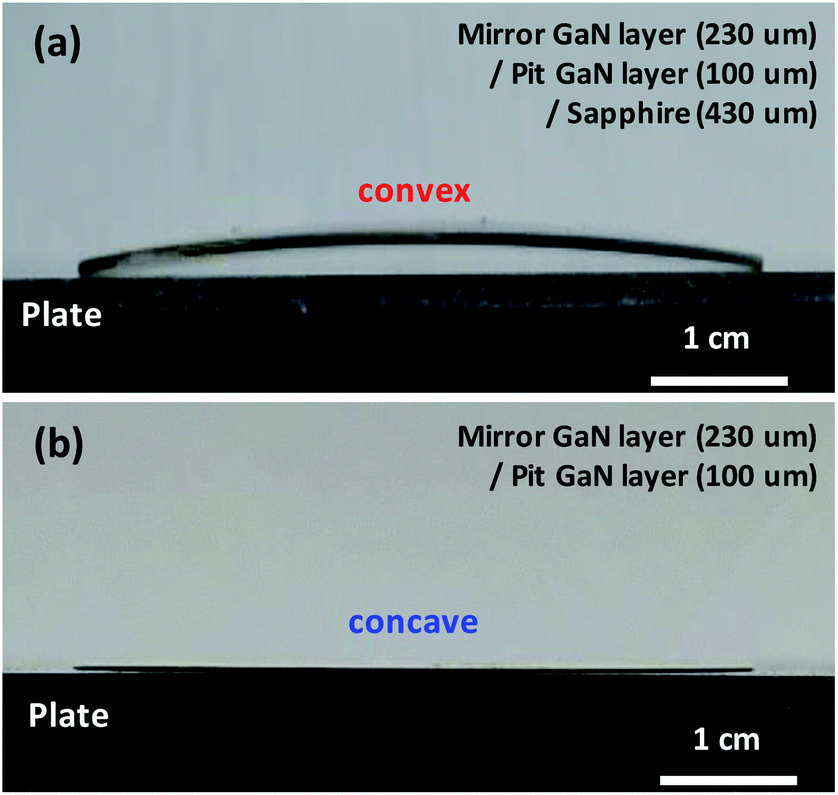
In HVPE growth, a ∼430 μm-thick sapphire substrate was heated to 990 °C under a N2 atmosphere so that the sapphire substrate diameter was expanded 0.73%. Note that the thermal expansion coefficient of the sapphire substrate was 7.5 × 10⁻⁶ K−1. Then, a ∼100 μm-thick pit GaN layer was grown by flowing HCl (1800 sccm) and NH3 (19600 sccm) gases at 990 °C. The grown pit GaN layer at the interface between the pit GaN layer and the sapphire substrate received a remarkable tensile strain, while the sapphire substrate at the interface accepted a considerable compressive strain since the lattice constant of the pit GaN layer (a = 3.18926 Å) was smaller than that of the sapphire substrate (a = 4.758 Å). Afterward, a ∼230 μm-thick mirror GaN layer was grown by flowing HCl (1000 sccm) and NH3 (2000 sccm) gases at 990 °C. Remembering that the pit GaN layer was a highly porous structure while the mirror GaN layer was a highly dense structure, thus the grown mirror GaN layer at the interface between the pit and the mirror GaN layers was put under tensile stress, while the pit GaN layer at the interface received a compressive stress. After the mirror GaN layer growth, during cooling down to room temperature, the sapphire substrate was much more highly shrunken than the pit and mirror GaN layers since the TEC of the sapphire substrate (7.5 × 10⁻⁶ K−1) was higher than that of the pit and mirror GaN layers (5.59 × 10⁻⁶ K−1). As a result, the pit GaN layer at the interface between the pit GaN layer and sapphire substrate received a remarkable tensile stress, while the sapphire substrate at the interface experienced a considerable compressive stress. In addition, the pit GaN layer at the interface between the pit and mirror GaN layers received a remarkable compressive stress, while the mirror GaN layer interface accepted a considerable tensile stress. Thus, the mirror GaN layer grown on the pit GaN layer on the sapphire substrate produced an extremely high remaining total-tensile-stress so that and it resulted in a highly convex wafer bow of 800–815 μm, as shown in Fig. 1(a). After HVPE growth, the mirror GaN layer grown on the pit GaN layer was separated from the sapphire substrate via LLO. Remembering that the LLO supplies extremely high energy to the interface between the pit GaN layer and sapphire substrate containing a high density of dislocations so that the interface is separated by a crack process, the separated pit GaN layer at the interface between pit and mirror GaN layers received a much higher tensile stress, while the separated mirror GaN layer at the interface accepted a very high compressive stress, since the remarkable compressive stress of the pit GaN layer at the interface between the pit GaN layer and sapphire substrate prior to the LLO was released from a high tensile stress of the sapphire substrate at the interface between the pit GaN layer and sapphire substrate prior to the LLO. As a result, the 230 μm-thick mirror GaN layer grown on the 100 μm-thick pit GaN layer produced a remarkably high remaining total-compressive-stress and it resulted in a highly concave wafer bow of −124 to −300 μm, as shown in Fig. 1(b). In order to investigate the dependency of the bow and residual stress of the polished GaN wafer with a mirror GaN layer and pit GaN layer as a function of the polishing-removal thickness of the mirror GaN layer after the first polishing step using 3 μm-diameter diamond abrasives, the 230 μm-thick mirror GaN layer with a concave wafer bow of −300 μm was used, as shown in Fig. 2.
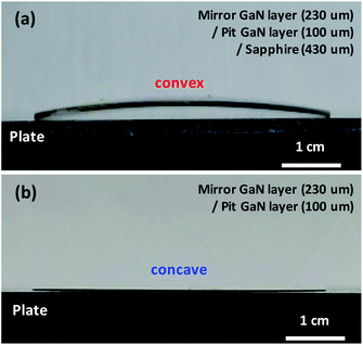 |
| | Fig. 1 Optical images of a wafer bow: (a) mirror GaN layer grown on a pit GaN layer on a sapphire substrate and (b) mirror GaN layer grown on a pit GaN layer. | |
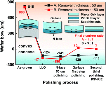 |
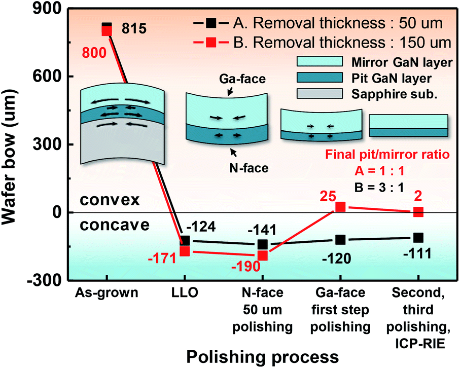
| | Fig. 2 Dependency of GaN wafer bow on the fabrication process followed by LLO, N-face pit GaN layer polishing of −50 μm, first Ga-face mirror GaN layer polishing of 50 or 150 μm, second Ga-face mirror GaN layer polishing of 2 μm, third Ga-face mirror GaN layer polishing of 1 μm, and ICP-RIE of ∼1 μm. | |
GaN wafer bow change during the wafering process
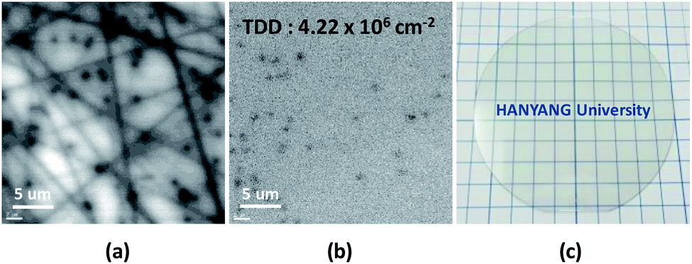
To fabricate a bow-free freestanding GaN wafer, process optimizations of pit GaN layer polishing, mirror GaN layer polishing, and inductively-coupled-plasma reactive-ion etching (ICP-RIE) were conducted, as shown in Fig. 2. The convexities of two as-grown GaN wafers were 800 and 815 μm after successive epitaxial growth of a pit GaN layer of 100 μm and an epitaxial mirror GaN layer of 230 μm. After the LLO, the 800 μm convexity of the as-grown GaN wafer changed to a concavity of −171 μm (sample A), while the 815 μm convexity of the as-grown GaN wafer was changed to a concavity of −124 μm (sample B). To eliminate the LLO-induced stripe pattern on the N-face pit layer, both samples A and B were subjected to N-face GaN layer polishing of ∼50 μm. Note that the LLO-induced stripe pattern on the N-face pit layer should be removed since it results in a photolithography inability. After the N-face GaN layer polishing of ∼50 μm, the bows of A and B became −190 μm and −141 μm concave, respectively. Referencing the dependency of GaN wafer bow on the polishing-removal thickness of the Ga-face mirror layer after the first polishing step using 3 μm-diameter diamond abrasives, sample A underwent Ga-face mirror GaN layer polishing of 150 μm, while B underwent Ga-face mirror GaN layer polishing of 50 μm, resulting in a convexity of +25 μm for A and −120 μm for B. These results indicate that a proper polishing-removal thickness could significantly suppress the GaN wafer bow and change the bow shape from concave to convex. The second polishing step of 2 μm using 0.5 μm-diameter diamond abrasives reduced the depth of the SSD from 1.1 μm (i.e., the first-step-polishing-induced SSD depth) to 0.5 μm, as shown in Fig. 3. Furthermore, ICP-RIE completely removed the third-step-polishing-induced SSD, as shown in Fig. 4. The third polishing step of the mirror layer induced many micro-scratches (i.e., straight black lines) and a high density of threading dislocations (i.e., dark spots), resulting in cracks and surface peeling during fabricating HB-LEDs, as shown in the SEM-CL image in Fig. 4(a). However, the ICP-RIE of the Ga-face mirror layer, i.e., ∼1 μm, eliminated micro-scratches and considerably reduced the threading dislocation density by up to 4.22 × 106 cm2, as shown in Fig. 4(b). Note that a conventional chemical-mechanical-planarization (CMP) using a colloidal-silica-abrasive or ceria-abrasive-based slurry could not reduce the surface roughness of the Ga-face surface and produced many scratches, as shown in Fig. S6,† since the colloidal-silica-abrasives had a spherical shape with a size of 40–100 nm, while the ceria-abrasives had an octahedral shape having sharp facets with a size of ∼80 nm. Thus, both samples A and B after the first polishing step of the Ga-face mirror layer were subjected to a second polishing step of this layer followed by a third step and ICP-RIE. The second (∼2 μm removal), third (∼1 μm removal), and ICP-RIE (∼1 μm removal) reduced the thickness of the GaN mirror layer by about 4 μm, changing the wafer bow of the GaN wafers. As a result, sample A consisted of a ∼148 μm-thick mirror GaN layer on a ∼50 μm-thick pit GaN layer, while sample B was made of a ∼48 μm-thick mirror GaN layer on a ∼50 μm-thick pit GaN layer. In sample A, the thickness of the mirror GaN layer (∼148 μm) was much thicker than that of the pit GaN layer (∼50 μm), sustaining the concave wafer bow and slightly reducing the wafer concave bow from −120 to −111 μm, as shown in Fig. 2. In contrast, in sample B, the thickness of the mirror GaN layer (∼48 μm) was slightly less than that of the pit GaN layer (∼50 μm), slightly reducing the wafer bow from 25 to 2 μm, as shown in Fig. 2. Again, this result implies that a reasonable polishing removal thickness could considerably help control the wafer bow.
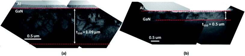 |
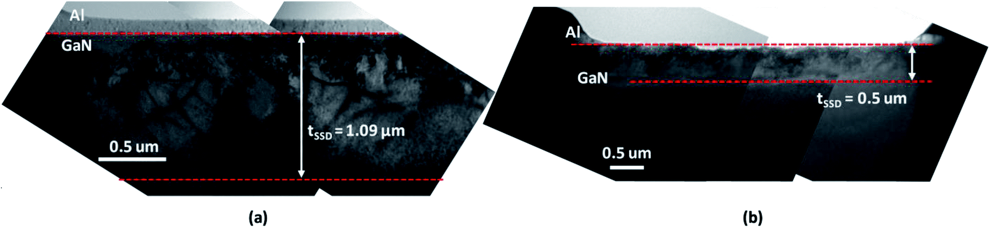
| | Fig. 3 Cross-sectional TEM (x-TEM) images of the subsurface damaged layer (SSD) of a Ga-face mirror GaN layer surface in a polished GaN wafer after (a) first polishing step using 3 μm-diameter diamond abrasives and (b) second polishing step using 0.5 μm-diameter diamond abrasives. Many dislocations and cracks remained in the SSD layer. Al layer was deposited to protect the GaN wafer surface during x-TEM sample preparation. | |
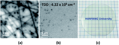 |
| | Fig. 4 SEM-CL images of Ga-face mirror GaN layer (a) after the third polishing step (b) after ICP-RIE, and (c) image of 2-inch bow-free freestanding GaN wafer. | |
Relationship between subsurface damage and the wafer bow
In the polishing process to eliminate scratches and to reduce surface roughness, the Ga-face mirror GaN layer surface in a polished GaN wafer is inevitably damaged by the diamond abrasives because of the mechanical collision between this surface and the diamond abrasives. This damaged surface is called the subsurface damaged layer (SSD).27 The cross-sectional transmission electron microscopy (x-TEM) images of the mirror GaN layer surface in the polished GaN wafer after the first and second polishing steps exhibited many polishing-induced dislocations and lateral cracks remaining in the damaged subsurface of the mirror GaN layer surface in the polished GaN wafer, as shown in Fig. 3. The SSD depths after the first and second polishing steps were about 1.1 and 0.5 μm, respectively. This difference in SSD depths after the first and second polishing steps was due to the different abrasive sizes in the polishing slurry, i.e., 3 and 0.5 μm for those steps, respectively.
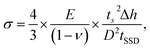
The bow of a GaN wafer is determined mainly by the residual stress of the polished GaN wafer thickness, i.e., less residual stress in a polished wafer leads to less GaN wafer bow. To understand the dependency of residual stress on the polishing-removal thickness of the mirror GaN layer surface in a polished GaN wafer after the first polishing step, the residual stress of a polished GaN wafer was calculated using the following Stoney's formula,28
| |
 | (1) |
where
σ is the residual stress of a polished GaN wafer,
ts is the thickness of a polished GaN wafer,
E is the Young's modulus of GaN,
ν is Poisson's ratio,
D is the diameter of a GaN wafer,
tSSD is the thickness of the SSD, and Δ
h is the GaN wafer bow.
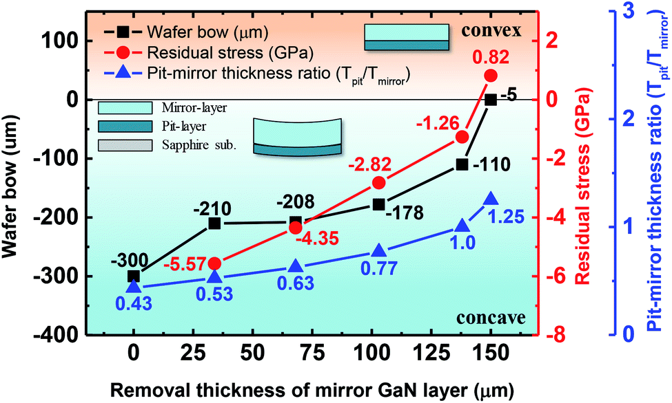
Fig. 5 shows the GaN wafer bow change during the mirror GaN layer polishing process. The initial bow of the GaN wafer was −300 μm; however, it decreased to −210, −208, −178, −110, and −5 μm, while 34, 68, 103, 138, and 150 μm of the mirror GaN layer was removed by the polishing process, respectively. At the same time, the residual stress of the GaN wafer calculated by
eqn (1) when 34, 68, 103, 138, and 150 μm of mirror GaN layer removed was −5.57 GPa and decreased simultaneously to −4.35, −2.82, −1.26, and 0.82 GPa, respectively. When 150 μm of mirror GaN layer was removed, the GaN wafer showed a concave bow (−5 μm), but the sign of the calculated residual stress was changed from negative to positive. This result showed a good relation between the degree of bow and the calculated residual stress;
i.e., the magnitude of concave bow decreased with the increasing removal thickness of a mirror GaN layer since the remaining compressive stress decreased with increasing the removal thickness of a mirror GaN layer. In addition, the thickness ratio between the pit and mirror GaN layers is a key parameter to determine the achievement of a bow-free wafer, as shown in
Fig. 5. It is worth remembering that, after the LLO, the strain of the mirror layer was compressive while the strain of the pit layer was tensile. In addition, the total strain of the mirror layer grown on the pit layer was compressive, meaning that the magnitude of the compressive strain in the mirror layer was considerably higher than the tensile strain in the pit layer. The thickness ratio between the pit and mirror layers increased with the polishing-removal thickness of the Ga-face mirror layer. Thus, the remaining compressive strain stress of the mirror GaN layer grown on the pit GaN layer decreased with increasing the thickness ratio between the pit and mirror layers. In particular, when the thickness ratio increased from 1.0 to 1.25, the remaining strain of the mirror GaN layer grown on the pit GaN layer was changed from compressive (
i.e., −1.26 GPa) to tensile strain (
i.e., 0.82 GPa). This result indicates that there is a specific thickness ratio to achieve a bow-free status of the mirror GaN layer grown on the pit GaN layer;
i.e., ∼1.15
:
1. Therefore, the design of the thickness ratio between the pit and mirror layers would be a key research area for obtaining bow-free wafers.
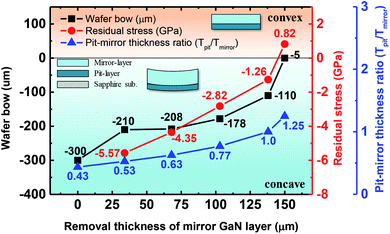 |
| | Fig. 5 GaN wafer bow, residual stress, and pit-mirror thickness ratio depending on the polishing-removal thickness of Ga-face mirror layer after the first polishing step using 3 μm-diameter diamond abrasives. Note that GaN wafer consisted of a 230 μm-thick Ga-face mirror layer and 100 μm-thick pit layer after LLO. Only the 230 μm-thick Ga-face mirror layer was polished. | |
Surface inspection (roughness and scratch)
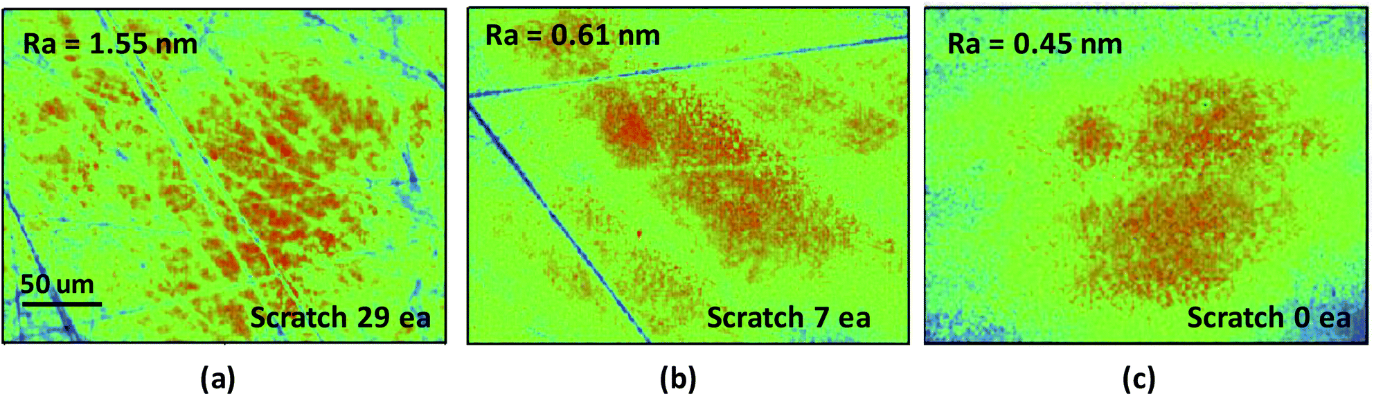
We also investigated the scratches using white-light interferometry images on the mirror GaN layer surface of a GaN wafer after the first, second, and third steps of the polishing process using diamond abrasives of 3 μm, 0.5 μm, and 50 nm, respectively, as shown in Fig. 6. Note that the separated GaN wafer via LLO was followed by the first, second, and third steps in the polishing process of the mirror GaN layer surface to eliminate subsurface polishing damage and to control GaN wafer bow. We found that the surface roughness of the mirror GaN layer surface of the polished GaN wafer decreased from 1.55 to 0.61 then to 0.45 nm, and the number of scratches on that surface decreased from 29 to 7 then to 0 ea by the three-step polishing process. These results indicate that a smaller diamond abrasive leads to fewer remaining scratches and a low surface roughness. However, a smaller diamond abrasive performs at a slower polishing rate; thus, from the viewpoint of a cost-effective fabrication process, the three-step polishing process is necessary for achieving a scratch-free surface and low surface roughness of a freestanding GaN wafer. Furthermore, the optical property of our researched GaN wafer in Fig. 4(c) was examined by PL, presenting the peak wavelength between 364.8–365.2 nm in wavelength (average 365 nm) and a full-width at half-maximum (FWHM) between 7.1–7.6 nm (average 7.35 nm), as shown in Fig. S7.†
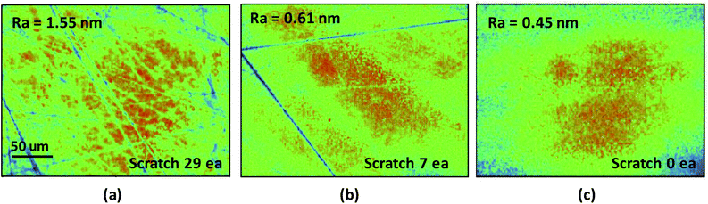 |
| | Fig. 6 White-light interferometry images for scratches and surface roughness after (a) first polishing step using 3 μm-diameter diamond abrasives, (b) second polishing step using 0.5 μm-diameter diamond abrasives, and (c) third polishing step using 50 nm-diameter diamond abrasives of a Ga-face mirror-layer surface in a polished GaN wafer. Three-step polishing was continuously conducted. | |
Conclusions
A GaN wafer grown on a sapphire substrate by HVPE exhibited an extremely highly convex bow. After LLO to separate the GaN wafer from a sapphire substrate, the GaN wafer bow changed to a considerable concave shape. Thus, N-face polishing of the pit layer, three-step polishing, and ICP-RIE of the Ga-face mirror layer are essential for fabricating bow-free freestanding GaN wafers. The LLO-induced stripe patterns should be removed by the N-face polishing of the pit layer for optical extraction efficiency of HB LEDs, slightly increasing the concavity. The polishing-removal thickness of the Ga-face mirror layer in the first polishing step using 3 μm-diameter diamond abrasives could mainly control the GaN wafer bow, i.e., the concavity of the GaN wafer gradually decreased with increasing the polishing-removal thickness of the Ga-face mirror layer in the first polishing step since the compressive stress of the polished GaN wafer after the first polishing step was also almost linearly decreased with increasing the polishing-removal thickness of the Ga-face mirror layer. The second polishing step of the Ga-face mirror layer using 0.5 μm-diameter diamond abrasives and the third polishing step of the Ga-face mirror layer using 50 nm-diameter diamond abrasives could eliminate micro-scratches on that layer. Finally, ICP RIE of the mirror GaN layer could completely remove third-step-polishing-induced damage. Thus, the process-design comprising LLO, pit GaN layer polishing, three-step-polishing, and ICP-RIE of the Ga-face mirror layer enabled the fabrication of 2-inch-diameter bow-free freestanding GaN wafers for application in HB-LEDs.
Conflicts of interest
There are no conflicts to declare.
Acknowledgements
This work was financially supported by the Brain Korea 21 Plus Program in 2019.
Notes and references
- Y. Narukawa, M. Ichikawa, D. Sanga, M. Sano and T. Mukai, J. Phys. D: Appl. Phys., 2010, 43, 354002 CrossRef.
- M. J. Cich, R. I. Aldaz, A. Chakraborty, A. David, M. J. Grundmann, A. Tyagi, M. Zhang, F. M. Steranka and M. R. Krames, Appl. Phys. Lett., 2012, 101, 223509 CrossRef.
- G. Li, W. Wang, W. Yang, Y. Lin, H. Wang, Z. Lin and S. Zhou, Rep. Prog. Phys., 2016, 79, 056501 CrossRef PubMed.
- D. S. Joag, D. J. Late and U. D. Lanke, Solid State Commun., 2004, 130, 305–308 CrossRef CAS.
- B. Chitara, D. J. Late, S. B. Krupanidhi and C. N. R. Rao, Solid State Commun., 2010, 150, 2053–2056 CrossRef CAS.
- E. Oh, S. K. Lee, S. S. Park, K. Y. Lee, I. J. Song and J. Y. Han, Appl. Phys. Lett., 2001, 78, 273–275 CrossRef CAS.
- J. A. Freitas Jr, J. C. Culbertson, N. A. Mahadik, T. Sochacki, M. Boćkowski and M. Iwinska, Cryst. Growth Des., 2015, 15, 4837–4842 CrossRef.
- A. Tanaka, W. Choi, R. Chen, R. Liu, W. M. Mook, K. L. Jungjohann, P. K. L. Yu and S. A. Dayeh, J. Appl. Phys., 2019, 125, 082517 CrossRef.
- B. P. Yonkee, E. C. Young, C. Lee, J. T. Leonard, S. P. DenBaars, J. S. Speck and S. Nakamura, Opt. Express, 2016, 24, 7816 CrossRef CAS PubMed.
- M. Lee, M. Yang, K. M. Song and S. Park, ACS Photonics, 2018, 5, 1453 CrossRef CAS.
- S. S. Park, I.-W. Park and S. H. Choh, Jpn. J. Appl. Phys., 2000, 39, L1141 CrossRef CAS.
- K. Fujito, S. Kubo, H. Nagaoka, T. Mochizuki, H. Namita and S. Nagao, J. Cryst. Growth, 2009, 311, 3011–3014 CrossRef CAS.
- P. Visconti, K. M. Jones, M. A. Reshchikov, F. Yun, R. Cingolani, H. Morkoç, S. S. Park and K. Y. Lee, Appl. Phys. Lett., 2000, 77, 3743–3745 CrossRef CAS.
- D. Ehrentraut, R. T. Pakalapati, D. S. Kamber, W. Jiang, D. W. Pocius, B. C. Downey, M. McLaurin and M. P. D'Evelyn, Jpn. J. Appl. Phys., 2013, 52, 08JA01 CrossRef.
- M. Imade, M. Imanishi, Y. Todoroki, H. Imabayashi, D. Matsuo, K. Murakami, H. Takazawa, A. Kitamoto, M. Maruyama, M. Yoshimura and Y. Mori, Appl. Phys. Express, 2014, 7, 035503 CrossRef.
- N. Liu, J. Wu, W. Li, R. Luo, Y. Tong and G. Zhang, J. Cryst. Growth, 2014, 388, 132–136 CrossRef CAS.
- E. V. Etzkorn and D. R. Clarke, J. Appl. Phys., 2001, 89, 1025–1034 CrossRef CAS.
- K. Yamane, T. Matsubara, T. Yamamoto, N. Okada, A. Wakahara and K. Tadatomo, J. Appl. Phys., 2016, 119, 045707 CrossRef.
- F. Lipski, M. Klein, X. Yao and F. Scholz, J. Cryst. Growth, 2012, 352, 235–238 CrossRef CAS.
- R. Quay, Gallium Nitride Electronics, Springer, Leipzig, 2008 Search PubMed.
- Y. Dai, Y. Shao, Y. Wu, X. Hao, P. Zhang, X. Cao, L. Zhang, Y. Tian and H. Zhang, RCS Adv., 2014, 4, 21504 CAS.
- Y. Oshima, T. Eri, M. Shibata, H. Sunakawa and A. Usui, Phys. Status Solidi A, 2002, 194, 554–558 CrossRef CAS.
- N. Okada, H. Ihara, K. Yamane and K. Tadatomo, Phys. Status Solidi B, 2016, 253, 819–823 CrossRef CAS.
- R. Singh, I. Radu, G. Bruederl, C. Eichler, V. Haerle, U. Gösele and S. H. Christiansen, Semicond. Sci. Technol., 2007, 22, 418–421 CrossRef CAS.
- F.-M. Hsiao, M. Schnedler, V. Portz, V.-C. Huang, B.-C. Huang, M.-C. Shih, C.-W. Chang, L.-W. Tu, H. Eisele, R. E. Dunin-Borkowski, Ph. Ebert and Y.-P. Chiu, J. Appl. Phys., 2017, 121, 015701 CrossRef.
- J. Cho, Z. Li, E. Bozorg-Grayeli, T. Kodama, D. Francis, D. H. Altman, F. Ejeckam, F. Faili, M. Asheghi and K. E. Goodson, presented in part at the 37th Annual GOMACTech Conference, Las Vegas, March, 2012 Search PubMed.
- H. Aida, H. Takeda, S.-W. Kim, N. Aota, K. Koyama, T. Yamazaki and T. Doi, Appl. Surf. Sci., 2014, 292, 531–536 CrossRef CAS.
- G. G. Stoney, Proc. R. Soc. London, Ser. A, 1909, 82, 172–175 CAS.
Footnote |
| † Electronic supplementary information (ESI) available: Images of HVPE GaN growth and lapping system, OM, SEM, CL, AFM and TEM data. See DOI: 10.1039/d0ra01024c |
|
| This journal is © The Royal Society of Chemistry 2020 |
Click here to see how this site uses Cookies. View our privacy policy here. 
 Open Access Article
 This Open Access Article is licensed under a Creative Commons Attribution-Non Commercial 3.0 Unported Licence
 *
*