
 Open Access Article
 This Open Access Article is licensed under a Creative Commons Attribution-Non Commercial 3.0 Unported Licence
High stability and visible-light photocatalysis in novel two-dimensional monolayer silicon and germanium mononitride semiconductors: first-principles study†
Kaining Zhang and
Nan Li *
*
State Key Laboratory of Explosion Science and Technology, School of Mechatronical Engineering, Beijing Institute of Technology, Beijing 100081, P. R. China. E-mail: leen04@163.com; Tel: +86-10-68914863
First published on 8th April 2020
Abstract
Recently, two-dimensional semiconductor materials with moderate band gaps and significant light absorption have been highly sought for application in photocatalysis and nanoelectronics. In this study, novel monolayer SiN and GeN have been predicted by using first-principles calculations. They have excellent thermal and dynamic stabilities and present indirect band gaps of 2.58 eV and 2.21 eV with anisotropic carrier mobility, respectively. Suitable band gaps and band edges of SiN and GeN indicate that they can simultaneously produce both hydrogen and oxygen in the pH range of 6 to 14 and 0 to 10, respectively. Theoretical studies on strain engineering show that their band gaps could be effectively tuned by both biaxial tensile and compressive strain. Our work enriches the family of two-dimensional semiconductor materials and shows that monolayer SiN and GeN are promising candidates for electronic devices and photocatalysis.
1. Introduction
Two-dimensional (2D) atomic layered materials have attracted tremendous interest due to their extraordinary chemical and physical properties, and they have great potential application in the photocatalysis and nanoelectronic fields.1–3 Graphene possesses excellent thermal conductivity, high carrier mobility and other exotic properties.4–6 However, graphene lacks a band gap, which limits its application in semiconductor technology. This defect motivated the search for novel 2D materials. In recent years, some 2D materials, including, but not limited to, black phosphorene (BP),7 transition-metal dichalogenides (TMDs),8–10 monolayer group IV,11 monolayer group V,12,13 and monolayer group III monochalcogenides,14,15 have been explored. Due to the high carrier mobility and direct band gap, BP is emerging as a contender in the field of 2D materials.16,17 The monolayer TMDs, represented by MoS2, with a direct band gap and excellent stability, are promising candidates for electronic devices.18,19 Furthermore, some of the 2D materials put forward by early theoretical researches have been synthesized experimentally even without a natural parent material afterwards, like silicone and germanene.20,21 Therefore, the theoretical study is always the forerunner to discover more novel 2D materials.Recently, monolayer silicon and germanium monopnictide MX (M = Si and Ge; X = P and As) with the space group of C2/m has been theoretically studied.22 They are proved to be stable which have the band gaps of 2.02–2.64 eV lying in the visible light region. Among these MX materials, 2D SiP, GeP and GeAs have been synthesized experimentally.23–29 The devices based on these three materials exhibit anisotropic behaviors and photocatalytic activity, indicating their great potential for anisotropy optoelectronic and photocatalytic applications. In theoretical studies, the monolayer SiAs has a high carrier mobility up to 8.98 × 103 cm2 V−1 s−1, which is much higher than that of silicon (about 1.40 × 103 cm2 V−1 s−1).30,31 The designed monolayer SiAs and GeAs also present great photocatalysis potential for water splitting with appropriate band edge positions.30 A detailed comparison of the activation barriers for various possible paths in the interlayer region of bilayer GeP indicates that Li atom can diffuse about 50 times faster than in the graphene bilayer, making it highly desirable for application as lithium-ion batteries electrode.32 Through absorbing different 3d transition metal (TM) atoms on monolayer MX without magnetic, the corresponding TM–MX shows various magnetic moments, which might have potentials in spintronics and magnetoelectric devices.33 Moreover, the electronic and optical properties of monolayer MX (M = Si and Ge; X = P and As) can be accurately turned by uniaxial or biaxial strain.34–37 Thus, monolayer MX can be a potential candidate in high speed electronic devices and photocatalysis. Due to the electronic structure with 1s22s22p3, the nitrogen (N) is relatively small in size and large in electronegativity. Replacing the elements of 2D materials by N always brings interesting properties,38,39 such as the newly synthesized 3R-MoN2, isotypic with rhombohedral R3m MoS2.40 It presents three times more active than the MoS2 for the hydrodesulfurization of dibenzothiophene and twice as high in the selectivity to hydrogenation. The monolayer MN (M = Si and Ge) with the space group of C2/m is unexplored. The N atoms may lead to a host of interesting physical and chemical properties of significant utility, such as novel electronic structures, which might be beneficial for applications in optoelectronic and electronic devices.
In this work, the structures, stabilities, electronic properties, photocatalysis, and strain engineering of monolayer (ML) MN (M = Si, Ge) with the space group of C2/m are investigated using first-principles calculations in this study. The calculation results prove the dynamic and thermal stabilities of the ML SiN and GeN. They possess indirect band gaps of 2.58 eV and 2.21 eV, respectively, which can be accurately tuned by homogeneous biaxial tensile and compressive strain. Moreover, ML GeN has the perfect band edge positions for both producing hydrogen and oxygen simultaneously from a pH range of 0 to 10 and high optical absorbance. The ML SiN can produce hydrogen and oxygen from a pH range of 6 to 14. These excellent properties illustrate that ML SiN and GeN can be the promising materials for photocatalysis and electronic devices.
2. Methods
In this study, first-principles calculations are performed by using density-functional theory (DFT) with projector-augmented wave (PAW) potentials to study the electronic structures by the Vienna Ab initio Simulation Package (VASP).41–43 The generalized gradient approximation (GGA) with the Perdew–Burke–Ernzerhof (PBE) functional44 is adopted for exchange-correlation energy. To obtain more accurate band gaps, the Herd–Scuseria–Ernzerhof hybrid functional (HSE06) is employed to calculate band structures and the standard mixing fraction is set to 0.25 for the exact exchange.45 For all geometric optimizations and electronic structure calculations, the energy cutoff for the plane-wave basis is set to 500 eV. The convergence criteria of energy and Hellmann–Feynman force for the ionic relaxation are set at 10−5 eV and 0.01 eV Å−1, respectively. The Brillouin zone sampling is used the Monkhorst–Pack scheme with 3 × 17 × 1 and 5 × 27 × 1 k-point grids for the geometry optimizations and electronic properties calculations, respectively. To obtain the band structures, 60 uniform k-points along the high symmetric lines in the first Brillouin zone are used. A vacuum space of 20 Å is employed for the monolayers along the z direction to avoid the interlayer interactions. The valence electron configurations of the N, Si and Ge atoms are 2s23p3, 3s23p2 and 4s24p2, respectively. Phonon dispersion spectra are obtained by using the finite displacement method utilized in the PHONOPY code46 with 1 × 6 × 1 supercell sheets. The thermal stabilities of these two novel nitrides in 1 × 5 × 1 supercells are obtained by performing ab initio molecular dynamics (AIMD) simulations by VASP software. The simulations at the temperature of 300 K, 800 K and 1000 K last for 5 ps with a time step of 1 fs, which are controlled by using the Nosé heating bath scheme.47 For strain engineering, the strain value can be defined as , where b0 and b are the lattice constants of these two novel nitrides before and after structure deformation, respectively. Then, the carrier effective masses are calculated by the formula m* = ℏ2(∂2E/∂k2)−1, where E is the energy eigenvalue; k is the wave vector and ℏ is the reduced Planck constant.
3. Results and discussion
3.1 Structural and stability
The structures of ML MN (M = Si and Ge) is shown in Fig. 1a and b, with the space group of C2/m (no. 12). They both contain 12 M atoms and 12 N atoms in the rectangular unit cell. Each M atom is coordinated to three N atoms and one M atom, and each N atom bonds to three neighboring M atoms. The optimized lattice parameters of ML SiN and GeN are a = 17.449 Å and 18.947 Å, and b = 2.956 Å and 3.118 Å, respectively. | ||
| Fig. 1 (a) Top and (b) side view of ML MN (M = Si, Ge). The unit cell is shown by the black rectangle. (c) Brillouin zone of ML MN with high symmetric points. | ||
To investigate the dynamic stabilities of ML SiN and GeN, the phonon dispersion spectra along high symmetric lines in the first Brillouin zone are calculated, as shown in Fig. 2a and b. The highest frequency modes of ML SiN and GeN are about 977 cm−1 and 751 cm−1, respectively, which are much larger than that of SiP (400 cm−1)48 and GeP (300 cm−1),22 indicating the large mechanical robustness of the M–N bonds. The phonon dispersion spectra show no imaginary phonon mode in Brillouin zone except for a very small pocket near Γ point. This small pocket of instability in the flexural phonon branch is not a real physical effect, while they reveal the difficulty of achieving numerical convergence in the flexural phonon branch for 2D material.49 The above results suggest the dynamic stability of ML SiN and GeN.
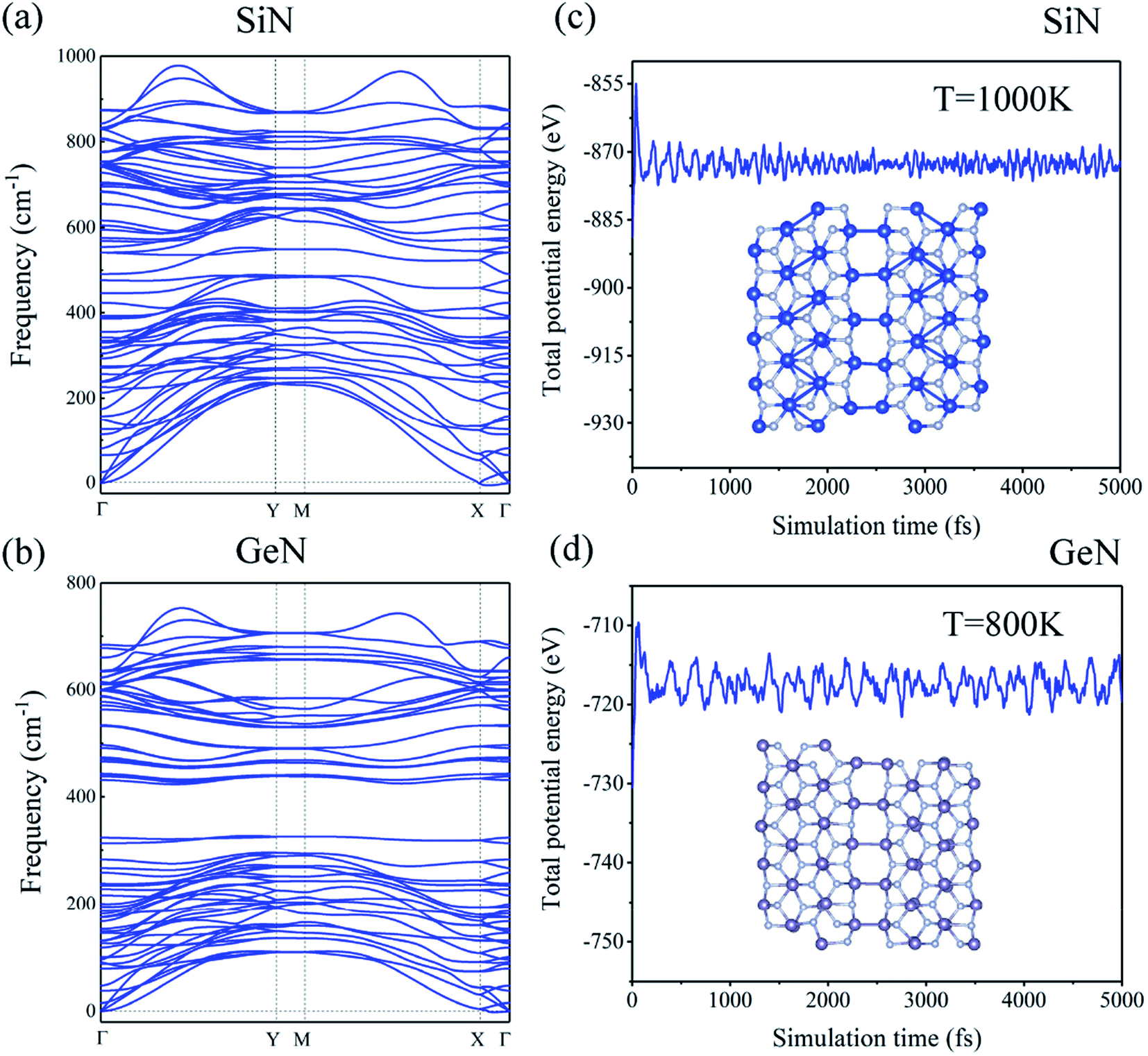 | ||
| Fig. 2 Phonon dispersion spectra of MLs (a) SiN, (b) GeN. The evolution of total energies of MLs (c) SiN, (d) GeN from AIMD simulations. The insets show snapshots of supercells at the end of 5 ps. | ||
To further examine the thermal stabilities of these two novel nitrides, the AIMD simulations are performed at room temperature (300 K, see Fig. S1†) and elevated temperatures (800 K and 1000 K) for 5 ps with a time step of 1 fs. The time-dependent evolution of total potential energies and selected snapshots of these two novel nitrides are shown in Fig. 2c and d. Even at a temperature as high as T = 1000 K, the total potential energy of ML SiN fluctuates smoothly with small amplitude and there is no bond breaking or significant structural reconstruction during the simulation, indicating the excellent thermal stability of ML SiN. The ML GeN maintains its structural stability at the temperature of 800 K during the simulation (see Fig. 2d), while its structure is deformed with the broken GeGe2 bonds (defined in Fig. 1) at the temperature of 1000 K (see Fig. S1†).
Based on the calculated phonon dispersion spectra and AIMD simulations, it is evident that the ML SiN and GeN are dynamically and thermally stable, which can ensure the important feasibility of their successful fabrication in industrial applications.
3.2 Electronic properties
The band structures along high symmetric lines are calculated at both PBE and HSE06 levels of theory to explore the electronic properties of ML SiN and GeN. As shown in Fig. 3a and b, the ML SiN and GeN are semiconductors with indirect band gaps of 1.54 eV and 1.30 eV at the PBE level of theory. Using the more accurate HSE06 method, the band gaps of SiN and GeN are 2.58 eV and 2.21 eV, respectively, which lie in the visible light region. The obtained band gaps of SiN and GeN are smaller than ML SiP (2.64 eV) and GeN (2.31 eV) at the HES06 level of theory, respectively.22 Compare the band gaps of MN (M = Si and Ge) and that of MP, an increase tendency in the band gaps of both SiX and GeX (X = N and P) can be observed with the increase of X atomic numbers. The mechanism behind this behavior is discussed in the ESI Note 1.† For both ML SiN and GeN, the valence band maximums (VBMs) are halfway between Γ and Y along the high symmetry line and the VBMs are all close to the Fermi level. On the contrary, the conduction band minimum (CBM) of ML GeN locates at Γ point, whereas the CBM of ML SiN at M point. In addition to the moderate band gaps, an impressive feature of these two novel nitrides is their significantly anisotropic band dispersion around the band gap. As displayed in Fig. 3, both the bottom of the conduction bands and the top of the valence bands are highly dispersed along the Γ–Y direction, while these bands are nearly flat along the Γ–X direction (except the CBM of ML GeN along the Γ–X direction). Therefore, the corresponding effective masses of electrons and holes are also highly anisotropic, as shown in Table 1, due to the inverse proportion relationship between curvature and effective masses. For different directions, the values of effective masses along Γ–X direction are several times higher than that along Γ–Y direction. For example, the effective masses of electron and hole of ML SiN along Γ–Y direction are 0.52m0 and 0.56m0, respectively, whereas effective masses of electron and hole along Γ–X direction are 1.14m0 and 3.77m0, respectively, m0 is the electron rest mass. In order to understand the above differently anisotropic band dispersion, the partial charge densities of ML SiN and GeN are plotted in Fig. 4. The results show that the spatial electron cloud of the bottom of the conduction bands along the y direction is continuous (marked as red rectangles in Fig. 4), which hints large mobility along this direction. Along other directions, the electron cloud is isolated in each unit cell with an inappreciable overlap (marked as black rectangles in Fig. 4), indicating low mobility along this direction.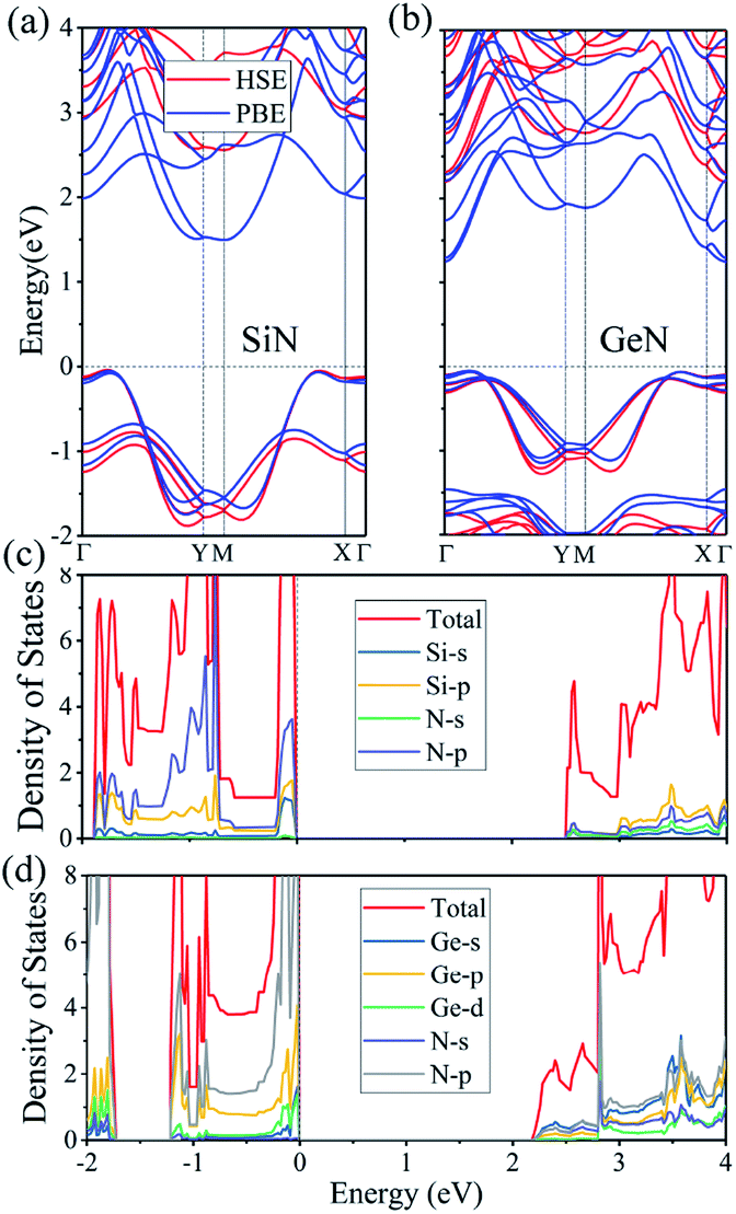 | ||
| Fig. 3 Band structures of MLs (a) SiN and (b) GeN at HSE06 (red line) and PBE (blue line) levels of theory. The horizontal dash line located at 0 eV represents the Fermi level. Partial density of states (PDOS) of MLs (c) SiN and (d) GeN at HSE06 level of theory. | ||
| MLs | Electron | Hole | ||
|---|---|---|---|---|
| Γ–Y | Γ–X | Γ–Y | Γ–X | |
| SiN | 0.52 | 1.14 | 0.56 | 3.77 |
| GeN | 0.31 | 0.55 | 1.02 | 2.10 |
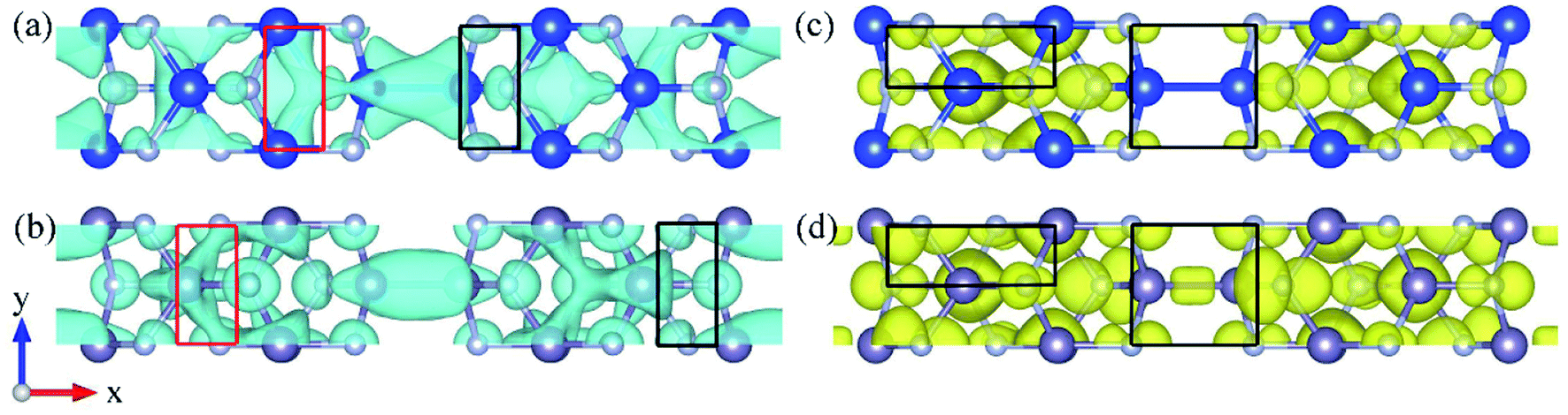 | ||
| Fig. 4 Partial charge densities of the ML SiN: (a) CBM (c) VBM from the top view with an isosurface of 0.0025 e Å−3, respectively. Partial charge densities of the ML GeN: (b) CBM and (d) VBM from the top view with an isosurface of 0.0012 e Å−3, respectively. | ||
The partial density of states (PDOS) are also computed to gain a deep insight into their band structures, as shown in Fig. 3c and d. The VBM of ML SiN is mainly contributed to the hybridized 3p orbitals of Si atoms and 2p orbitals of N atoms. Similar to ML SiN, the VBM of ML GeN is mainly contributed to the 4p of Ge and 2p orbitals of N. For the CBM of ML SiN and GeN, the N atoms contribute their 2p orbitals, while the characters of contributed orbitals of Ge and Si are different. The Si atoms contribute their 3p orbitals for the CBM band but the Ge atoms do their 4s orbitals.
The ML SiN and GeN with the moderate band gaps and the light carrier effective masses can be quite promising candidates for high-performance electronic devices.
3.3 Photocatalysis
As is well-known, photocatalytic water splitting is an effective way for solar energy conversion and storage to satisfy the demand of energy.50 2D materials are promising photocatalysis materials with ideal maximal specific surface,51,52 and they can accelerate the migration of electrons and holes to the reaction interfaces.53,54 In principle, two requirements should be fulfilled for a prospective water-splitting photocatalyst: a moderate band gap (lager than 1.23 eV) and suitable band edge positions straddling redox potentials of water.55 The standard redox potentials at pH = 0 are −5.67 eV for oxidation potential of O2/H2O and −4.44 eV for reduction potential of H+/H2. According to the Nernst equation, the redox potentials will increase with pH and the relationship can be expression: EH+/H2 = (−4.44 + pH × 0.059) eV and EO2/H2O = (−5.67 + pH × 0.059) eV.56 In present research, the pH ranging from 0 to 14 is studied.The band edge positions of these two novel nitrides and the redox potentials under different pH values are displayed in Fig. 5. In the case of ML SiN, both the VBM and CBM are higher than oxidation potential of O2/H2O and reduction potential of H+/H2 at pH = 0, respectively, which demonstrates that the ML SiN is photocatalytically active for hydrogen production. With the increase of pH from 0 to 6 in reaction system, the oxidation potential of O2/H2O is gradually close to the VBM, while the CBM is still higher than reduction potential of H+/H2. When pH increases from 6 to 14, the reduction potential and oxidation potential are involved in the band gap region, which means that the CBM of SiN is higher than reduction potential of H+/H2 and its VBM is lower than oxidation potential of O2/H2O. This suggests that the hydrogen and oxygen can be simultaneously produced on the surface of ML SiN and the photocatalytic capacity can be enhanced effectively by turning the pH value. For the case of ML GeN, its CBM and VBM are involved in the band gap region from a pH range of 0 to 10. This behavior indicates that GeN transfers the photoexcited electrons and holes to the water easily to produce both hydrogen and oxygen simultaneously. When pH > 10, the reduction potential of H+/H2 is moved beyond the CBM of GeN, indicating the absence of photocatalytic performance for hydrogen production.
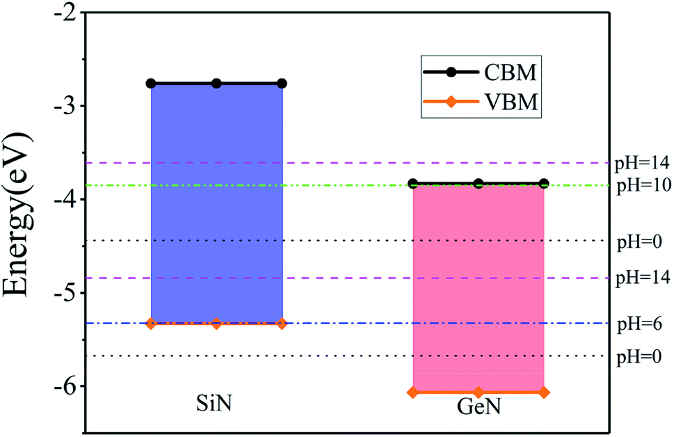 | ||
| Fig. 5 Band alignments of ML SiN and GeN relative to the vacuum energy level. The band edges are calculated by using HSE06 method. | ||
The appropriate band gaps and band edge positions of ML SiN and GeN inspire us to further explore their photon absorption properties. Therefore, we calculate the optical absorbance spectra A(ω) of the ML SiN and GeN by A(ω) = LωImε(ω)/c, where ω is the frequency of light, c is the speed of light in vacuum, L is the vacuum space of 20 Å between the isolated MN (M = Si and Ge) layers and Imε(ω) is imaginary part of the dielectric function calculated with the independent-particle approximation.57 Following the previous researches,58,59 we compensate for the band gap underestimation of the PBE functional by a rigid shift of the absorption curves upward by the value of the bandgap difference between the HSE06 and PBE functional, and the optical absorbance spectra are shown in Fig. 6. The optical absorbance spectra with different absorption behaviors for the polarized lights in different direction reveal the strong optical anisotropy of ML SiN and GeN. For ML SiN, it exhibits significant light absorption starting at around 2.6 eV. By contrast, the significant optical absorption of ML GeN starts at about 2.2 eV. Thus, the ML GeN has prior visible light absorption to ML SiN. In addition, the predicted optical absorbance attains to the maximum absorption of 25% for ML SiN and GeN, which are comparable with that of reported photocatalysts arsenene/Ca(OH)2 heterostructure.60 With appropriate band edges and high optical absorbance, ML SiN and GeN have promising potential to be optoelectronics devices and used in photocatalytic water splitting.
 | ||
| Fig. 6 Optical absorbance spectra A(ω) for MLs (a) SiN and (b) GeN. A(ω) are calculated using the PBE functional followed by a rigid energy shift to take into account the band gap underestimation of the PBE functional. | ||
3.4 Strain engineering
It has been demonstrated that the electronic and optoelectronic properties of 2D materials can be both experimentally and theoretically controlled and modified by strain engineering.61,62 In this study, the electronic properties under mechanical strain of both ML SiN and GeN have been explored. To simplify this issue, we employ the homogeneous biaxial strain model and study the electronic properties of ML SiN and GeN under the strain ranging from −5% to 5%. Due to the rigid band shift between PBE and HSE06, the band gap of ML SiN and GeN under biaxial strain are calculated using the PBE method in the following discussion.63The total energies of ML GeN and SiN as functions of strain are summarized in Fig. 7a, in which the strain energies increase monotonously with the increase of compressive and tensile strain. The geometries of the systems can return to their original states when the strains are removed, indicating that deformation of GeN and SiN is elastic.64 Fig. 7b shows the variation of band gap of ML GeN and SiN versus biaxial strain. Their gap value can be modulated monotonously from 0.77 eV to 2.01 eV and from 1.47 eV to 0.52 eV for −5% ≤ ε ≤ 5%, respectively. Meanwhile, their CBM and VBM remain at original high symmetric points and thus the indirect gap feature is not disturbed. The band structures of these two novel nitrides under strain are plotted in Fig. 7c. It is found that the VBM of ML SiN and GeN are insensitive to biaxial strain and always lie near the Fermi level. The CBM of the ML SiN shifts upward with the increase of tensile strain and shifts downward with compressive strain, while the CBM of ML GeN presents the opposite trend, which shifts downward with the increase of tensile strain and shifts upward with compressive strain. This opposite trend results in the opposite trend of their band gaps variation. To gain a deep insight into this opposite trend under strain, the atomic-orbital-projected band structures (AOPBS) and the crystal orbitals schematics are plotted in Fig. 8. The results show that the bottom of the conduction band of ML SiN is mainly based on the 3py orbitals of Si and 2pz orbitals of N. Around the M point, the 3py orbitals of Si have strong bonding interaction with those of the Si atoms above and below along the y direction (see Fig. 8c). This interaction can be increased by the compression strain along y direction, leading to the decrease of the energy of CBM and pushing down CBM at the M point. Therefore, the compression strain narrows the band gap, whereas the tensile strain enlarges the gap value. For ML GeN, the bottom of the conduction band of ML GeN is at Γ point and mostly made of the 4s orbitals of Ge and a small contribution of the 2pz orbitals of N. Thus, the energy of CBM is mainly decided by the 4s orbital of Ge, whose stability can be increased/decreased with the decrease/increase of GeGe2 bond lengths (the bond lengths are defined in Fig. 1) along z direction (see Fig. 8d). The GeGe2 bonds which are parallel to the z direction become shorter under homogeneous biaxial tensile strain (see Table 2), which increase the interaction between the 4s orbitals of Ge and lead to the decrease of the energy of CBM and CBM's pushing down at the Γ point. Thus, the biaxial tensile strain narrows the band gap.
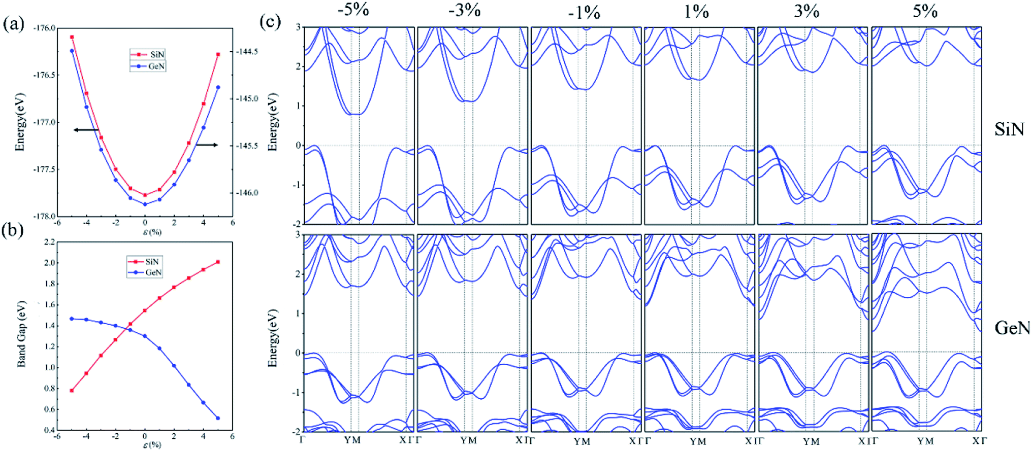 | ||
| Fig. 7 (a) Total energies and (b) the variation of band gap as functions of biaxial strain. (c) Band structures of the ML SiN and GeN under biaxial strain in the range of −5% to 5%. | ||
 | ||
| Fig. 8 Atomic-orbital-projected band structures of ML (a) SiN and (b) GeN with the biaxial strain of −5% (left panels), 0 (middle panels) and 5% (right panels). The sizes of the red, green, blue and magenta dots present the weights of the s, px, py and pz orbitals of Si, Ge and N, respectively. Without the biaxial strain, the crystal orbitals schematic of the bottom of the conduction band of (c) ML SiN at M point and (d) ML GeN at Γ point, respectively. | ||
| Bond | d0/Å | d5%/Å |
|---|---|---|
| GeGe1 | 2.488 | 2.716 |
| GeGe2 | 2.482 | 2.450 |
| GeN1 | 1.974 | 1.991 |
| GeN2 | 1.949 | 1.975 |
| GeN3 | 1.927 | 1.967 |
| GeN4 | 1.924 | 1.963 |
In a word, the electronic properties of the ML SiN and GeN can be prominently adjusted by the biaxial strain to meet future requirements of electronic devices.
4. Conclusions
In summary, we have investigated the structures, stabilities, electronic properties, photocatalysis, and strain engineering of the ML SiN and GeN by using first-principles calculations. Their dynamic and thermal stability are confirmed by both phonon dispersion spectra and AIMD. The moderate band gaps of 2.58 eV (SiN) and 2.21 eV (GeN) indicate that the ML SiN and GeN are attractive semiconductors for future applications in nanoelectronics. The band gap and band edges of ML GeN are suitable to produce hydrogen and oxygen from a pH range of 0 to 10, and its maximum optical absorbance is about 25%. This absorbance is comparable with that of reported photocatalysts arsenene/Ca(OH)2 heterostructure, indicating the ML GeN a promising candidate for photocatalytic water splitting. The SiN can produce hydrogen and oxygen from a pH range of 6 to 14 with optical absorbance as high as that of ML GeN. In addition, strain engineering can drastically tune the band gaps of these two novel nitrides. The band gap of ML SiN is found to monotonously increase under tensile strain but decrease when compressive strains are applied, while the ML GeN present an opposite trend. The composition of conduction band bottoms between monolayer SiN and GeN are different, resulting in their opposite trend of band gap under the biaxial strain. These two novel nitrides nanosheets with high stability, moderate band gaps, excellent light absorption are expected to show great application potential in electronic, sensors, photocatalysis, and energy conversion field. Moreover, our results provide guidance for experimentally synthesizing ML SiN and GeN.Conflicts of interest
There are no conflicts to declare.Acknowledgements
We are indebted to the National Natural Science Foundation of China (U1530262).References
- M. Chhowalla, D. Jena and H. Zhang, Two-dimensional semiconductors for transistors, Nat. Rev. Mater., 2016, 1, 16052 CrossRef CAS.
- B. N. Shivananju, W. Yu, Y. Liu, Y. Zhang, B. Lin, S. Li and Q. Bao, The roadmap of graphene-based optical biochemical sensors, Adv. Funct. Mater., 2017, 27, 1603918 CrossRef.
- S. Yang, Y. Liu, M. Wu, L.-D. Zhao, Z. Lin, H.-c. Cheng, Y. Wang, C. Jiang, S.-H. Wei, L. J. Huang, Y. Huang and X. Duan, Highly-anisotropic optical and electrical properties in layered SnSe, Nano Res., 2018, 11, 554–564 CrossRef CAS.
- K. S. Novoselov and A. K. Geim, The rise of graphene, Nat. Mater., 2007, 6, 183–191 CrossRef PubMed.
- F. Schwierz, Graphene transistors, Nat. Nanotechnol., 2010, 5, 487 CrossRef CAS PubMed.
- K. S. Novoselov, A. K. Geim, S. Morozov, D. Jiang, M. I. Katsnelson, I. Grigorieva, S. Dubonos and A. A. Firsov, Two-dimensional gas of massless Dirac fermions in graphene, Nature, 2005, 438, 197 CrossRef CAS PubMed.
- M. Buscema, D. J. Groenendijk, S. I. Blanter, G. A. Steele, H. S. Van Der Zant and A. Castellanos-Gomez, Fast and broadband photoresponse of few-layer black phosphorus field-effect transistors, Nano Lett., 2014, 14, 3347–3352 CrossRef CAS PubMed.
- B. Radisavljevic, A. Radenovic, J. Brivio, V. Giacometti and A. Kis, Single-layer MoS2 transistors, Nat. Nanotechnol., 2011, 6, 147 CrossRef CAS PubMed.
- D. Braga, I. Gutiérrez Lezama, H. Berger and A. F. Morpurgo, Quantitative determination of the band gap of WS2 with ambipolar ionic liquid-gated transistors, Nano Lett., 2012, 12, 5218–5223 CrossRef CAS PubMed.
- S. Tongay, W. Fan, J. Kang, J. Park, U. Koldemir, J. Suh, D. S. Narang, K. Liu, J. Ji, J. Li, R. Sinclair and J. Wu, Tuning interlayer coupling in large-area heterostructures with CVD-grown MoS2 and WS2 monolayers, Nano Lett., 2014, 14, 3185–3190 CrossRef CAS PubMed.
- C.-C. Liu, H. Jiang and Y. Yao, Low-energy effective Hamiltonian involving spin-orbit coupling in silicene and two-dimensional germanium and tin, Phys. Rev. B: Condens. Matter Mater. Phys., 2011, 84, 195430 CrossRef.
- J. Qiao, X. Kong, Z.-X. Hu, F. Yang and W. Ji, High-mobility transport anisotropy and linear dichroism in few-layer black phosphorus, Nat. Commun., 2014, 5, 4475 CrossRef CAS PubMed.
- M. Pumera and Z. Sofer, 2D monoelemental arsenene, antimonene, and bismuthene: beyond black phosphorus, Adv. Mater., 2017, 29, 1605299 CrossRef PubMed.
- S. Demirci, N. Avazlı, E. Durgun and S. Cahangirov, Structural and electronic properties of monolayer group III monochalcogenides, Phys. Rev. B, 2017, 95, 115409 CrossRef.
- K. Cheng, Y. Guo, N. Han, X. Jiang, J. Zhang, R. Ahuja, Y. Su and J. Zhao, 2D lateral heterostructures of group-III monochalcogenide: potential photovoltaic applications, Appl. Phys. Lett., 2018, 112, 143902 CrossRef.
- F. Xia, H. Wang and Y. Jia, Rediscovering black phosphorus as an anisotropic layered material for optoelectronics and electronics, Nat. Commun., 2014, 5, 4458 CrossRef CAS PubMed.
- G. Hu, T. Albrow-Owen, X. Jin, A. Ali, Y. Hu, R. C. Howe, K. Shehzad, Z. Yang, X. Zhu and R. I. Woodward, Black phosphorus ink formulation for inkjet printing of optoelectronics and photonics, Nat. Commun., 2017, 8, 278 CrossRef PubMed.
- Q. H. Wang, K. Kalantar-Zadeh, A. Kis, J. N. Coleman and M. S. Strano, Electronics and optoelectronics of two-dimensional transition metal dichalcogenides, Nat. Nanotechnol., 2012, 7, 699 CrossRef CAS PubMed.
- X. Xu, W. Yao, D. Xiao and T. F. Heinz, Spin and pseudospins in layered transition metal dichalcogenides, Nat. Phys., 2014, 10, 343 Search PubMed.
- Z. L. Liu, M. X. Wang, C. Liu, J. F. Jia, P. Vogt, C. Quaresima, C. Ottaviani, B. Olivieri, P. D. Padova and G. L. Lay, The fate of the 2√3 × 2√3 R(30°) silicone phase on Ag(111), APL Mater., 2014, 2, 075131 Search PubMed.
- M. Houssa, G. Pourtois, V. V. Afanasev and A. Stesmans, Electronic properties of two-dimensional hexagonal germanium, Appl. Phys. Lett., 2010, 96, 183 CrossRef.
- A.-Q. Cheng, Z. He, J. Zhao, H. Zeng and R.-S. Chen, Monolayered silicon and germanium monopnictide semiconductors: excellent stability, high absorbance, and strain engineering of electronic properties, ACS Appl. Mater. Interfaces, 2018, 10, 5133–5139 CrossRef CAS PubMed.
- C. Li, S. Wang, C. Li, T. Yu, N. Jia, J. Qiao, M. Zhu, D. Liu and X. Tao, Highly sensitive detection of polarized light using a new group IV–V 2D orthorhombic SiP, J. Mater. Chem. C, 2018, 6, 7219–7225 RSC.
- L. Li, W. Wang, P. Gong, X. Zhu, B. Deng, X. Shi, G. Gao, H. Li and T. Zhai, 2D GeP: an unexploited low-symmetry semiconductor with strong in-plane anisotropy, Adv. Mater., 2018, 30, 1706771 CrossRef PubMed.
- K. Doyeon, K. Park, F. Shojaei, T. T. Debela, I. S. Kwon, I. H. Kwak, J. Seo, J. P. Ahn, J. Park and H. S. Kang, Thickness-dependent bandgap and electrical properties of GeP nanosheets, J. Mater. Chem. A, 2019, 7, 16526–16532 RSC.
- T. Yu, H. Nie, S. Wang, B. Zhang, S. Zhao, Z. Wang, J. Qiao, B. Han, J. He and X. Tao, Two-dimensional GeP-based broad-band optical switches and photodetectors, Adv. Opt. Mater., 2019, 1901490 Search PubMed.
- S. Yang, Y. Yang, M. Wu, C. Hu, W. Shen, Y. Gong, L. Huang, C. Jiang, Y. Zhang and P. M. Ajayan, Highly in-plane optical and electrical anisotropy of 2D germanium arsenide, Adv. Funct. Mater., 2018, 28, 1707379 CrossRef.
- C. S. Jung, D. Kim, S. Cha, Y. Myung, F. Shojaei, H. G. Abbas, J. A. Lee, E. H. Cha, J. Park and H. S. Kang, Two-dimensional GeAs with a visible range band gap, J. Mater. Chem. A, 2018, 6, 9089–9098 RSC.
- J. Guo, Y. Liu, Y. Ma, E. Zhu, S. Lee, Z. Lu, Z. Zhao, C. Xu, S. J. Lee, H. Wu, K. Kovnir, Y. Huang and X. Duan, Few-layer GeAs field-effect transistors and infrared photodetectors, Adv. Mater., 2018, 30, 1705934 CrossRef PubMed.
- R. Meng, X. Sun, D. Yang, J. Bao and X. Chen, Two dimensional XAs (X= Si, Ge, Sn) monolayers as promising photocatalysts for water splitting hydrogen production with high carrier mobility, Appl. Mater. Today, 2018, 13, 276–284 CrossRef.
- F. Li, X. Liu, Y. Wang and Y. Li, Germanium monosulfide monolayer: a novel two-dimensional semiconductor with a high carrier mobility, J. Mater. Chem. C, 2016, 4, 2155–2159 RSC.
- F. Shojaei and H. S. Kang, Electronic structure of the germanium phosphide monolayer and Li-diffusion in its bilayer, Phys. Chem. Chem. Phys., 2016, 18, 32458–32465 RSC.
- S. Li, M. Zhou, F. Zheng and P. Zhang, Magnetic 3d transition metal atomic chains modulated by the intrinsic valley structure in MX monolayer, Adv. Electron. Mater., 2019, 5, 1800450 CrossRef.
- S. Kansara, P. D. Bhuyan, Y. Sonvane and S. K. Gupta, Two-dimensional silicon phosphide: low effective mass and direct band gap for future devices applications, J. Mater. Sci., 2019, 54, 11878–11888 CrossRef CAS.
- B. Mortazavi and T. Rabczuk, Anisotropic mechanical properties and strain tuneable band-gap in single-layer SiP, SiAs, GeP and GeAs, Phys. E, 2018, 103, 273–278 CrossRef CAS.
- S. Bai, C.-Y. Niu, W. Yu, Z. Zhu, X. Cai and Y. Jia, Strain tunable bandgap and high carrier mobility in SiAs and SiAs2 monolayers from first-principles studies, Nanoscale Res. Lett., 2018, 13, 404 CrossRef PubMed.
- Q.-Y. Chen, C. Cao and Y. He, Optical anisotropy and strain tunable optical, electronic and structural properties in monolayer GeP: a computational study, Phys. E, 2019, 113, 172–180 CrossRef CAS.
- Q. Li, L. He, C. Sun and X. Zhang, Computational study of MoN2 monolayer as electrochemical catalysts for nitrogen reduction, J. Mater. Chem. C, 2017, 121, 27563–27568 CAS.
- J.-H. Lin, H. Zhang, X.-L. Cheng and Y. Miyamoto, Single-layer group IV-V and group V-IV-III-VI semiconductors: structural stability, electronic structures, optical properties, and photocatalysis, Phys. Rev. B, 2017, 96, 035438 CrossRef.
- S. Wang, H. Ge, S. Sun, J. Zhang, F. Liu, X. Wen, X. Yu, L. Wang, Y. Zhang, H. Xu, J. C. Neuefeind, Z. Qin, C. Chen, C. Jin, Y. Li, D. He and Y. Zhao, A new molybdenum nitride catalyst with rhombohedral MoS2 structure for hydrogenation applications, J. Am. Chem. Soc., 2015, 137, 4815–4822 CrossRef CAS PubMed.
- G. Kresse and J. Hafner, Ab initio molecular-dynamics simulation of the liquid-metal–amorphous-semiconductor transition in germanium, Phys. Rev. B: Condens. Matter Mater. Phys., 1994, 49, 14251 CrossRef CAS PubMed.
- G. Kresse and J. Furthmüller, Efficient iterative schemes for ab initio total-energy calculations using a plane-wave basis set, Phys. Rev. B: Condens. Matter Mater. Phys., 1996, 54, 11169 CrossRef CAS PubMed.
- G. Kresse and D. Joubert, From ultrasoft pseudopotentials to the projector augmented-wave method, Phys. Rev. B: Condens. Matter Mater. Phys., 1999, 59, 1758 CrossRef CAS.
- J. P. Perdew, K. Burke and M. Ernzerhof, Generalized gradient approximation made simple, Phys. Rev. Lett., 1996, 77, 3865 CrossRef CAS PubMed.
- A. V. Krukau, O. A. Vydrov, A. F. Izmaylov and G. E. Scuseria, Influence of the exchange screening parameter on the performance of screened hybrid functionals, J. Chem. Phys., 2006, 125, 224106 CrossRef PubMed.
- A. Togo, F. Oba and I. Tanaka, First-principles calculations of the ferroelastic transition between rutile-type and CaCl2-type SiO2 at high pressures, Phys. Rev. B: Condens. Matter Mater. Phys., 2008, 78, 134106 CrossRef.
- S. Nosé, A unified formulation of the constant temperature molecular dynamics methods, J. Chem. Phys., 1984, 81, 511–519 CrossRef.
- S. Zhang, S. Guo, Y. Huang, Z. Zhu, B. Cai, M. Xie, W. Zhou and H. Zeng, Two-dimensional SiP: an unexplored direct band-gap semiconductor, 2D Mater., 2017, 4, 015030 CrossRef.
- V. Zólyomi, N. Drummond and V. Fal'Ko, Electrons and phonons in single layers of hexagonal indium chalcogenides from ab initio calculations, Phys. Rev. B: Condens. Matter Mater. Phys., 2014, 89, 205416 CrossRef.
- W. Chen, X. Hou, X. Shi and H. J. Pan, Two-dimensional Janus transition metal oxides and chalcogenides: multifunctional properties for photocatalysts, electronics, and energy conversion, ACS Appl. Mater. Interfaces, 2018, 10, 35289–35295 CrossRef CAS PubMed.
- X. Wang, K. Maeda, A. Thomas, K. Takanabe, G. Xin, J. M. Carlsson, K. Domen and M. Antonietti, A metal-free polymeric photocatalyst for hydrogen production from water under visible light, Nat. Mater., 2009, 8, 76 CrossRef CAS PubMed.
- Y. Zhang, T. Mori, J. Ye and M. Antonietti, Antonietti, phosphorus-doped carbon nitride solid: enhanced electrical conductivity and photocurrent generation, J. Am. Chem. Soc., 2010, 132, 6294–6295 CrossRef CAS PubMed.
- G. Collins, E. Armstrong, D. McNulty, S. O'Hanlon, H. Geaney and C. O'Dwyer, 2D and 3D photonic crystal materials for photocatalysis and electrochemical energy storage and conversion, Sci. Technol. Adv. Mater., 2016, 17, 563–582 CrossRef CAS PubMed.
- J. Wu, M. Liu, K. Chatterjee, K. P. Hackenberg, J. Shen, X. Zou, Y. Yan, J. Gu, Y. Yang, J. Lou and P. M. Ajayan, Exfoliated 2D transition metal disulfides for enhanced electrocatalysis of oxygen evolution reaction in acidic medium, Adv. Mater. Interfaces, 2016, 3, 1500669 CrossRef.
- Y. Ji, M. Yang, H. Lin, T. Hou, L. Wang, Y. Li and S.-T. Lee, Janus structures of transition metal dichalcogenides as the heterojunction photocatalysts for water splitting, J. Phys. Chem. C, 2018, 122, 3123–3129 CrossRef CAS.
- V. Chakrapani, J. C. Angus, A. B. Anderson, S. D. Wolter, B. R. Stoner and G. U. Sumanasekera, Charge transfer equilibria between diamond and an aqueous oxygen electrochemical redox couple, Science, 2007, 318, 1424–1430 CrossRef CAS PubMed.
- L. Matthes, P. Gori, O. Pulci and F. Bechstedt, Universal infrared absorbance of two-dimensional honeycomb group-IV crystals, Phys. Rev. B: Condens. Matter Mater. Phys., 2013, 87, 035438 CrossRef.
- D. Kecik, E. Durgun and S. Ciraci, Optical properties of single-layer and bilayer arsenene phases, Phys. Rev. B, 2016, 94, 205410 CrossRef.
- R. Asahi, T. Morikawa, T. Ohwaki, K. Aoki and Y. Taga, Visible-light photocatalysis in nitrogen-doped titanium oxides, Science, 2001, 293, 269–271 CrossRef CAS PubMed.
- X.-H. Li, B.-J. Wang, X.-L. Cai, W.-Y. Yu, L.-W. Zhang, G.-D. Wang and S.-H. Ke, Arsenene/Ca(OH)2 van der Waals heterostructure: strain tunable electronic and photocatalytic properties, RSC Adv., 2017, 7, 44394–44400 RSC.
- C. H. Ho and Y. J. Chu, Bending photoluminescence and surface photovoltaic effect on multilayer InSe 2D microplate crystals, Adv. Opt. Mater., 2015, 3, 1750–1758 CrossRef CAS.
- X. Peng, Q. Wei and A. Copple, Strain-engineered direct-indirect band gap transition and its mechanism in two-dimensional phosphorene, Phys. Rev. B: Condens. Matter Mater. Phys., 2014, 90, 085402 CrossRef.
- J. Silva-Guillén, E. Canadell, F. Guinea and R. Roldán, Strain tuning of the anisotropy in the optoelectronic properties of TiS3, ACS Photonics, 2018, 5, 3231–3237 CrossRef.
- Q. Yue, S. Chang, J. Kang, S. Qin and J. Li, Mechanical and electronic properties of graphyne and its family under elastic strain: theoretical predictions, J. Phys. Chem. C, 2013, 117, 14804–14811 CrossRef CAS.
Footnote |
| † Electronic supplementary information (ESI) available. See DOI: 10.1039/d0ra00964d |
| This journal is © The Royal Society of Chemistry 2020 |