
 Open Access Article
 This Open Access Article is licensed under a Creative Commons Attribution-Non Commercial 3.0 Unported Licence
Fabrication of black aluminium thin films by magnetron sputtering†
J. More-Chevalier *a,
M. Novotnýa,
P. Hruškaab,
L. Feketea,
P. Fitlac,
J. Bulířa,
P. Pokornýa,
L. Volfováad,
Š. Havlováac,
M. Vondráčeka and
J. Lančoka
*a,
M. Novotnýa,
P. Hruškaab,
L. Feketea,
P. Fitlac,
J. Bulířa,
P. Pokornýa,
L. Volfováad,
Š. Havlováac,
M. Vondráčeka and
J. Lančoka
aInstitute of Physics of the Czech Academy of Sciences, Na Slovance 1999/2, 182 21 Prague, Czech Republic. E-mail: morechevalier@fzu.cz
bFaculty of Mathematics and Physics, Charles University, Ke Karlovu 3, 12116 Praha 2, Czech Republic
cDepartment of Physics and Measurements, University of Chemistry and Technology Prague, Technicka 5, 16628 Praha 6, Czech Republic
dFaculty of Science, Charles University, Hlavova 2030/8, 12843 Praha 2, Czech Republic
First published on 1st June 2020
Abstract
Black aluminium thin films were prepared by direct current (DC) pulsed magnetron sputtering. The N2 concentration in the Ar–N2 mixture that was used as the deposition atmosphere was varied from 0 to 10%, and its impact on the film growth and optical properties was studied. A strong change in the film growth process was observed as a function of the N2 concentration. At a specific N2 concentration of ∼6%, the Al film growth process favoured the formation of a moth-eye-like antireflective surface. This surface morphology, which was similar to the structure of a cauliflower, is known to trap incident light, resulting in films with a very low reflectivity. A diffuse reflectivity lower than 4% was reached in the ultraviolet-visible-near infrared (UV-VIS-NIR) spectral range that corresponds to a value observed for an ultrahigh absorber. We found that for the preparation of black aluminium, the nitrogen content plays an important role in film formation and the resulting film morphology.
1. Introduction
Metals with highly porous structures usually possess reduced reflectivity. These metals are often referred to as metal black or black metals (BMs).1 BM surface properties are rather specific and result from the combined effects of nanostructural, microstructural, and macrostructural features. BM coatings were first fabricated by the evaporation of bismuth at elevated pressures.2 To date, BMs have found applications in electronic devices for optical sensing and imaging, electrochemical sensing and solar cells;3–9 countermeasures; camouflage; engraving; and marking, for example.10,11 The utilization of BMs in sensing benefits from the fact that the surface area of BMs is much higher than the geometrical surface area, e.g., it is 60 m2 g−1 and 30 m2 g−1 for black palladium and platinum, respectively.8 BMs (i.e., platinum and gold) have been used to fabricate electrodes for electrochemical sensors.7,8,12Recently, a black aluminium (B-Al) coating was utilized to improve the energy conversion from a light source to an electrical current with the pyroelectric effect.13 Gold is one of the most common BMs, but it suffers from several unattractive properties, such as extremely low adhesion, low thermal stability, and low wear resistance. On the other hand, B-Al possesses several advantages, such as good wear resistance and good adhesion. B-Al can maintain its optical properties (e.g., a low reflection) at elevated temperatures exceeding 300 °C.14,15 Moreover, B-Al is very suitable for industrial utilization due to its low cost.
Several techniques capable of preparing BMs have been reported: (1) deposition by thermal evaporation (TE),2–5,14,16–19 (2) deposition by magnetron sputtering (MS),20–22 (3) electrodeposition,7,8,12 (4) thin metal film deposition on dielectric substrates with imprinted antireflective black silicon (BSi) moth-eye-like nanostructures,6,23 and (5) laser surface modification.10,11,24,25
Techniques (1) through (4) are suitable for the fabrication of BM thin films on large-area substrates, while technique (5) can only be used for the modification of either bulk materials or thin film surfaces over limited areas. Technique (3) usually leads to a less porous film than techniques (1) and (2)26 and requires highly toxic chemical precursors. Technique (4) is not universal because it requires that the deposition occurs on preprocessed silicon substrates. The surface of BMs prepared by techniques (1)–(4) can be easily modified by a localized nanosecond laser treatment that produces a glossy metal surface27,28 and enables the additional tuning of its functional properties. Technique (5) employs mostly femtosecond lasers10 and is time consuming, which is its major drawback.
TE and MS allow efficient tuning of the nano-, micro- and macrostructure via the variation of deposition conditions that directly affect the growth process, i.e. the composition and pressure of the working gas, temperature, and substrate orientation and angle. B-Al films were obtained by TE in hydrogen,17,19 helium14 and clean air18 atmospheres at pressures of 133–266 Pa (H2 and He) and 0.13–1.33 Pa (air).
Despite these facts and the obvious potential of MS toward BM preparation, it has been rarely reported. MS at oblique angles with a rotating substrate was used for black gold film fabrication.21,22
This paper reports on the preparation of B-Al film by direct current (DC) pulsed MS at room temperature. The influence of the nitrogen (N2) concentration in the argon–nitrogen mixture used during the deposition process on its growth and properties is discussed.
2. Experimental techniques
2.1 Film growth
The aluminium films were deposited by DC pulsed MS on glass substrates that were fixed on an unheated substrate holder placed at a distance of 100 mm from the target. The vacuum chamber was pumped down to a base pressure of 2 × 10⁻³ Pa. A round-shaped magnetron aluminium target (Al purity of 99.99%) with a diameter of 100 mm was used for sputtering. A DC power supply (Hüttinger 3000) combined with a pulse generator (MELEC) was operated at a power (Pd) of 400 W, repetition frequency (f) of 10 kHz and duty cycle of 0.5. The magnetron discharge was maintained in an Ar/N2 reactive atmosphere at a constant total pressure of 0.5 Pa that was regulated using a throttle valve at the high-vacuum pump gate. The Ar flow (QAr) was fixed at 16 sccm, and the N2 gas flow was varied from 0 to 1.2 sccm, where its partial pressure was varied from 0 Pa to 2 × 10⁻² Pa, which corresponds to the N2 percents varying from 0 to 11%. A series of samples were deposited that consisted of four groups. Reflective aluminium films (N2 = 0) were prepared and are referred to as R-Al. Then, B-Al films with different nitrogen percents from 2 to 4% were prepared and are referred to as B-Al 3%. The samples that have a nitrogen percent that ranges from 5 to 7% were prepared and are referred to as B-Al 6%. Those that have a nitrogen percent that ranges from 9 to 11% are referred to as B-Al 10%. The DC magnetron voltage varied from 283 V to 465 V for the R-Al and B-Al samples, respectively. The average film thickness was approximately 500 nm at a deposition rate of 80 nm min−1. The amount of the gas molecules (O2 and N2) and atoms (O and N) contained in the residual atmosphere of the deposition chamber were studied by mass spectrometry at conditions that are described in our previous work.292.2 Structural characterization
The crystallographic phases present in the samples were determined by the powder X-ray diffraction (XRD) method in the symmetrical Bragg–Brentano geometry on a D8 Discover (Bruker AXS, Germany) using Cu Kα radiation and a divergent beam. Quantitative Rietveld refinement was performed in TOPAS V5 to determine the wt% of all the identified phases following the published theory.30,312.3 Film surface pictures and chemical analysis
Atomic force microscopy (AFM) measurements were carried out at room temperature on an ambient atomic force microscope (Bruker, Dimension Icon) in peak force tapping mode with ScanAsyst air tips (Bruker; k = 0.4 N m−1; nominal tip radius of 2 nm) or classical tapping mode using Tap 150 Al-G tips (BudgetSensors; k = 5 N m−1; nominal tip radius < 10 nm) for samples with a high roughness. The measured topographies had a resolution of 512 × 512 pixels.2 Scanning electron microscopy (SEM) was conducted on a TESCAN FERA 3 GM operated at 15 kV to study the morphology of the samples. The scanning electron microscope was equipped with an EDAX Octane 60 mm2 energy dispersive spectroscopy (EDS) analyser that operated at 5 kV and was used to determine the chemical composition of the samples. The presented results are the average of 4 measurements performed on each sample. Core level X-ray photoelectron spectroscopy (XPS) was measured by a NanoESCA photoemission electron microscope (Omicron) using monochromatic Al Kα radiation.2.4 Optical characterization
Diffuse reflectance measurements were performed using a spectrophotometer (Specord 250, Analytik Jena) equipped with an integrating sphere. As the reference sample, we used the reflectance standard made of Spectralon (LabSphere).3. Results and discussion
3.1 Film crystallization
The XRD θ–2θ scans over the 2θ range from 30–90° from the R-Al and B-Al layers are shown in Fig. 1(a), and the 2θ range from only 35–50° is presented in Fig. 1(b). In the case of the R-Al layer (blue curve in Fig. 1), the observed peaks correspond to the diffraction pattern of the Al structure, represented by the black vertical lines in the figure, which is a member of the Fm![[3 with combining macron]](https://www.rsc.org/images/entities/char_0033_0304.gif) m group and has a lattice parameter a (Å) = 4.0490(7).32 Polycrystalline films are observed with four peaks in the analysis range at 2θ = 38.47(2)°, 44.72(1)°, 65.09(7)° and 78.22(9)°, which correspond to the (111), (200), (220) and (311) planes, respectively, that are parallel to the substrate. An analysis of the peak intensities reveals that the film also has a preferred (111) orientation. This texture is observed for each crystallized film, and the reason is discussed in part 3.4 of the manuscript.
m group and has a lattice parameter a (Å) = 4.0490(7).32 Polycrystalline films are observed with four peaks in the analysis range at 2θ = 38.47(2)°, 44.72(1)°, 65.09(7)° and 78.22(9)°, which correspond to the (111), (200), (220) and (311) planes, respectively, that are parallel to the substrate. An analysis of the peak intensities reveals that the film also has a preferred (111) orientation. This texture is observed for each crystallized film, and the reason is discussed in part 3.4 of the manuscript.
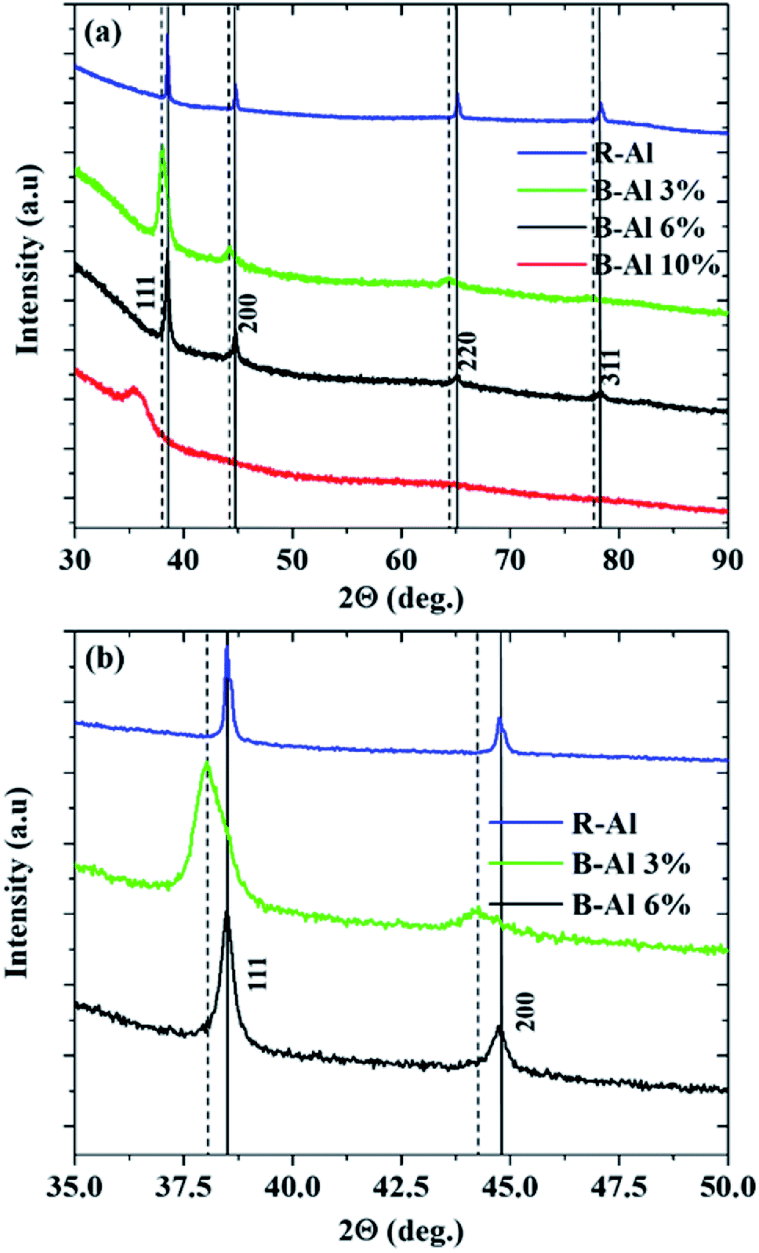 | ||
| Fig. 1 (a) XRD diffraction patterns from the R-Al and B-Al layers deposited on glass substrates as a function of N2 percent used during the deposition step and (b) the XRD pattern in the 2θ range from 35–50°. The full lines present the Al peaks from a structure with in the Fmm space group with a lattice parameter a (Å) = 4.0490(7). The dashed lines are Al peaks from the stressed structure with a larger lattice parameter of a (Å) = 4.0759(6). | ||
The B-Al film deposited with a N2 percent of 3% during the sputtering step (green curve in Fig. 1) presents a change in the shape of the peaks. Contrary to peaks from the R-Al film, two peaks can be distinguished and are shown in Fig. 1(b). The first peak (full vertical line) corresponds to the aluminum peak that is observed in the R-Al film. The second peak (dashed vertical line) also corresponds to an Al peak, but there is a difference in the lattice parameter a (Å) = 4.0759(6), which is expanded due to the tensile stress in this second Al phase. Many papers report a change in the intrinsic stress in polycrystalline metal films due to the presence of impurities.33–37 Cougnon and co-authors reported a linear increase in the intrinsic tensile stress in Al, Cr and Cu films as a function of the impurity/metal flux ratio varying from 0.1 to 1 during the deposition step on a Si substrate.37 This tensile stress disappears in the B-Al film deposited with a high N2 percent of 6%. Only peaks corresponding to an Al phase with no tensile strain are visible. The difference between the R-Al film and the B-Al 6% film is that the peak shapes are broader, indicating smaller grain sizes in the B-Al 6% film than in the R-Al film and a stronger misorientation between grains with the same orientation. The B-Al film deposited with a N2 percent of 10% exhibits no crystalline structure according to our measurements. The only broad peak observed between 2θ = 35° and 2θ = 37.5° corresponds to the diffuse scattering of the short-range internal order of the glass substrate.38
3.2 Surface morphology and chemical analysis
The morphology of the R-Al and B-Al film surfaces is presented in Fig. 2. A strong variation in the morphology is observed as a function of the N2 percent used during the deposition process. The R-Al film presents a rough surface with a rms = 40.2 nm and large crystals on the surface with an average size of 200 nm. An increase in the N2 percent to 3% modifies the film morphology of the B-Al film and results in a decreased roughness with an rms = 29.6 nm. The number of grains visible on the film surface suggests that a low coalescence occurs among them. Then, the B-Al film deposited with a N2 percent of 6% shows a different morphology with a rough surface and a rms = 93.1 nm. The surface structure morphology of the B-Al film deposited with a N2 percent of 6% exhibits a cauliflower nanostructure with spherical grains that are very similar to the structure of the B-Al coating reported in our previous work.13 In the case of the B-Al films deposited with a N2 percent of 10%, the film surface changes again in comparison to the previous sample. A smooth surface with a rms = 0.8 nm is obtained from the AFM image. No grains can be distinguished in the images, which is typical for amorphous layers.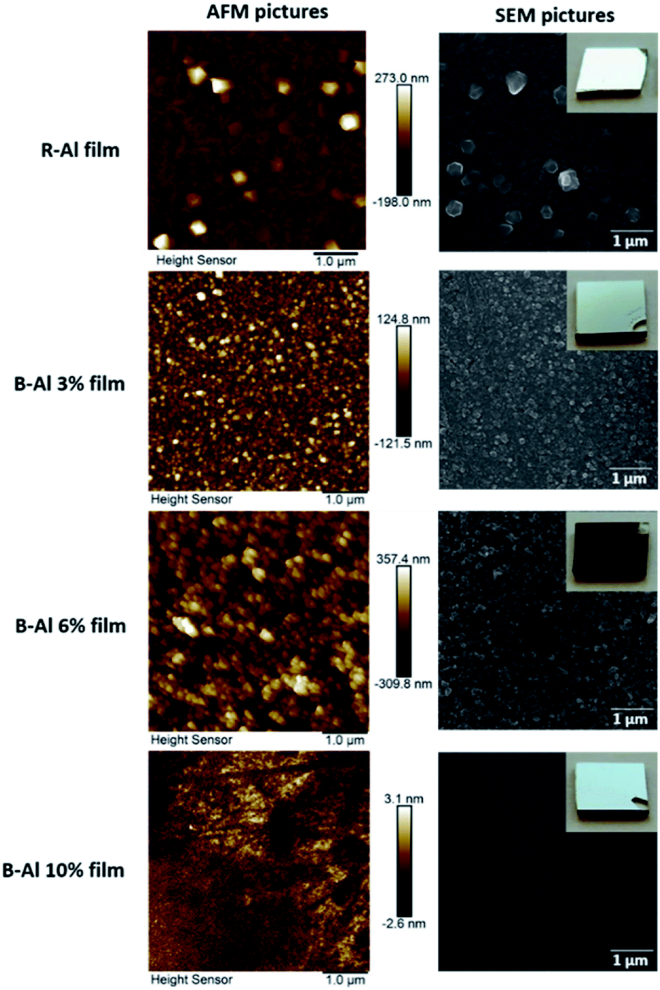 | ||
| Fig. 2 AFM and SEM images of the surface of the films as a function of the N2 percent from 0% to 10% during the deposition step. Optical images of each sample are inserted in the SEM images. | ||
The elemental composition of the Al films estimated by the EDS measurements is presented in Table 1. An average carbon contamination of ∼4% is observed on the film surfaces. We hypothesize that this contamination comes from reactions on the film surface that is freshly exposed to air after the deposition step.39 This is supported by XPS depth profile analyses presented in the ESI.†
| Content (at%) | Al film | B-Al 3% film | B-Al 6% film | B-Al 10% film |
|---|---|---|---|---|
| Al | 92.0 ± 2.5 | 79.0 ± 2.5 | 69.0 ± 2.0 | 58.0 ± 2.0 |
| O | 2.0 ± 1.5 | 6.0 ± 2.0 | 13.0 ± 2.0 | 1.5 ± 1.0 |
| N | 1.5 ± 1.0 | 8.0 ± 2.0 | 14.0 ± 2.0 | 38.0 ± 2.0 |
| C | 4.0 ± 2.0 | 5.0 ± 2.0 | 4.0 ± 2.0 | 2.5 ± 1.5 |
Then, an increase in the O and N concentrations is observed from the Al film to the B-Al film deposited with a N2 percent of 6%. This increase reflects the competition between the oxygen and nitrogen reactions that occur during the deposition step. The XPS spectrum of the B-Al film deposited with a N2 percent of 6% depicted in Fig. 3 reveals the presence of metallic aluminium, AlN and Al2O3; thus, the XPS results revealed the same content of nitrogen in the film as the EDX. The Al2O3 Gibbs free energy of formation of −1582.2 kJ mol−1 is ∼5.5 times faster than the AlN Gibbs free energy of formation of −287 kJ mol−1.40 Moreover, the relatively high base pressure of 2 × 10⁻³ Pa increases the oxygen contamination risk in comparison with a deposition chamber with a base pressure of 1 × 10⁻⁴ Pa or 1 × 10⁻⁵ Pa.38 Finally, for the B-Al film deposited with a N2 percent of 10%, the N2 gas introduced in the chamber becomes sufficiently high to statistically limit the oxygen reaction, and the final N concentration measured in the film is the majority, as reported in Table 1.
 | ||
| Fig. 3 XPS spectrum of Al 2p core level of B-Al 6% film. The experimental XPS data were fitted with a Shirley background and three unresolved into Al 2p Voigt doublets. The first one is from metallic aluminium, the second one is from AlN and the third one is from Al2O3. | ||
3.3 Diffuse reflectivity
A comparison of the diffuse reflectivity of the layers is presented in Fig. 4. The R-Al film presents an average reflectance (R) of 77.5% for wavelengths ranging from 350 nm to 1100 nm. The minimum R ∼ 70.5% corresponds to the absorbance peak observed at λ ∼ 828 nm.41–43 The absorption is related to the interband transitions at the W point of the Brillouin zone in the Al band structure. The reflectivity coming from the B-Al 3% film is strongly decreased in comparison to the previous sample, with a plateau at R ∼ 12% from λ ∼ 350 nm to 400 nm. Then, with increasing wavelength, the measured reflectivity increases nearly linearly until R ∼ 45% at 1100 nm. A similar trend was reported for B-Al deposited by TE.18 The optical property variation is associated with a change in the growth, which leads to a decrease in the surface roughness, as observed in the AFM and SEM images, which is certainly induced by the duality between both the Al phases measured by XRD and presented in Fig. 1. The reflectivity measured from the B-Al 6% film displays a very low reflectivity with an average R ∼ 3.7% in the visible-near infrared area. This result is comparable with the measured reflectance varying from 10 to 3% obtained by a laser surface texturing treatment or by reactive ion etching on metal films.6,11,24,44,45 A reflectance in the visible spectrum as low as 6% was reported for Al films deposited on BSi substrates previously structured by reactive ion etching.6 The high absorbance of the light was correlated to the columnar/cauliflower structure observed in the B-Al films. The nanostructure revealed by the AFM and SEM images presents patterns with dimensions smaller than the wavelength of the light used during the diffuse reflectivity measurements. The surface morphology traps the light and decreases the reflectance by a gradual variation in the refractive index from the air to Al, which is called the moth-eye effect. These types of surfaces present moth-eye antireflection surfaces.24,46 The diffuse reflectivity measured for the B-Al film deposited with 10% nitrogen increases in comparison to the previous B-Al film deposited with 6% nitrogen. The reflectivity varies from a R ∼ 18% at 350 nm to R ∼ 32% at λ ∼ 1100 nm. This dependence corresponds to the growth change resulting in the B-Al amorphous layer and the smooth surface on the B-Al 10% film.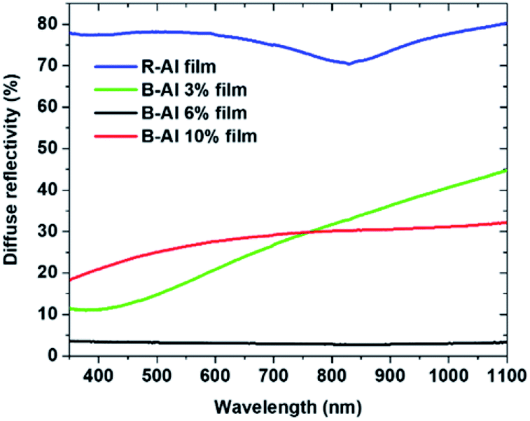 | ||
| Fig. 4 Diffuse reflectivity from R-Al and B-Al films as a function of the N2 percent used during the deposition step. | ||
3.4 Film growth
The presence of N2 in the plasma during the deposition step changes the growth of the Al film and modifies the optical properties. Each film was deposited at room temperature, which corresponds to a low deposition temperature in this situation, and the nucleation rate on the substrate is important. The film growth is described in Fig. 5 and divided into 3 steps. Fig. 5(a) shows the growth of the Al film, Fig. 5(b) shows the growth of the B-Al 3% film and Fig. 5(c) shows the growth of the B-Al deposited with 6% nitrogen. The polycrystalline Al layer grows according to the Volmer–Weber mechanism.38,47,48 The same nucleation step occurs on the surface of the substrate, as shown in Fig. 5, point (1).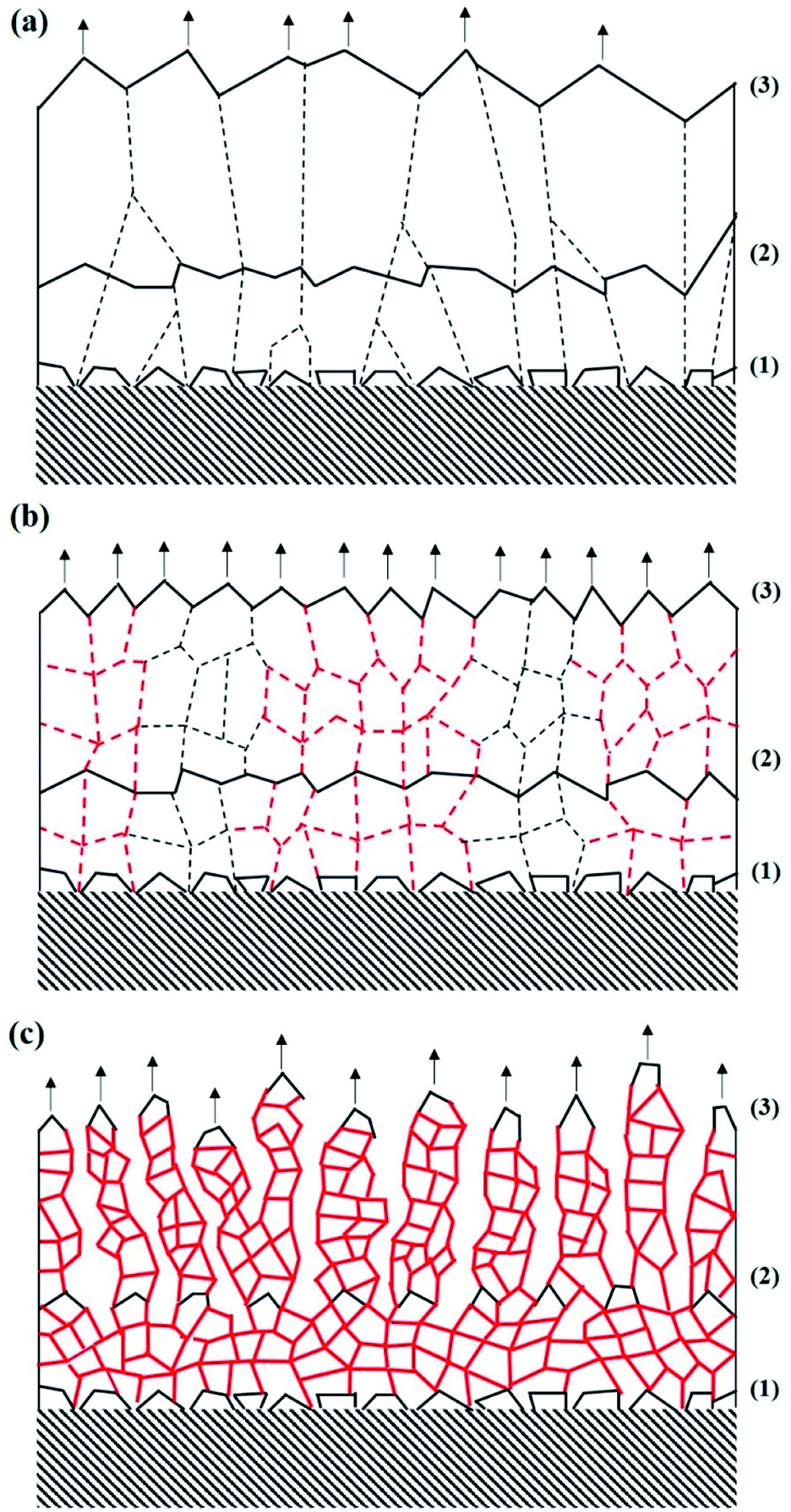 | ||
| Fig. 5 Schematics of film growth as a function of the N2 percent used in the deposition step: (a) the Al film growth representation, (b) B-Al 3% film growth representation, and (c) B-Al 6% film growth representation. Numbers on the right side of figures indicate the film growth step detailed in the text (part 3.4) where (1) is the nucleation step, (2) is the coalescence step, and (3) is the end of the film growth. The black dashed lines show standard grain boundaries, the red dashed lines are grain boundaries with a slight concentration of impurities, and the full red lines are grain boundaries with a high concentration of impurities. | ||
In the Al film shown in Fig. 5(a), island growth is followed by nuclei formation until grain coalescence occurs (point (2)). Due to the low deposition energy, the coarsening among grains is limited, and the mobility of the grain boundaries is slow. Therefore, a growth competition occurs mainly between nuclei with different structural orientations. A faster growth is observed for nuclei with a crystal orientation that minimizes the surface and interface energies between the crystal domain and the substrate/air surfaces. In the case of aluminium and materials crystallizing in the face-centred cubic (fcc) structure, the (111) preferred orientation is usually favoured during film growth, which is in good agreement with the XRD patterns shown in Fig. 1.47 At the end of the deposition step, the coalescence is finished, and the mechanism of columnar grain growth gives the characteristic shape as shown in Fig. 5(a) (point (3)).
When a small percentage of N2 gas is introduced into the working atmosphere during the deposition step, a change is observed in the growth of the B-Al 3% film, as presented in Fig. 5(b). After the first nucleation step at point (1), the growth competition between the nuclei with different structural orientations remains active. During the coalescence at point (2), as shown in Fig. 5(b), no coarsening processes occur among the grains, contrary to the behaviour of the Al film (Fig. 5(a)), due to impurities (oxygen and nitrogen) fixed in the grain boundaries. The increasing number of grain boundaries limits grain growth and grain size. Therefore, new nuclei tend to form on the grain surface, as described in Fig. 5(b) and at point (2). Finally, the nucleation and coalescence steps are reproduced infinitely until the end of the deposition step (Fig. 5(b) point (3)).
The reduction in the grain size decreases the film roughness, as measured by AFM in part 3.2, where a rms value of 40.2 nm was obtained for the Al film and 29.3 nm for the B-Al 3% film. This result is in good agreement with our previous work, where a smoother surface was observed on Al films deposited with an equivalent concentration of oxygen impurities that the global concentration of impurities in the B-Al 3% film.38,49,50
An intrinsic tensile stress in a part of the B-Al 3% layer occurs after film coalescence and is caused by the “zipping process” during grain boundary formation.36,37 The boundaries with a sufficiently high concentration of impurities to induce stress are shown as red dashed lines in Fig. 5(b). This effect has been studied and reported on several single elements, such as Al, Cu, and Cr, where a tensile stress was measured by XRD.37 In the paper by F. G. Cougnon et al., two regimes were reported. The first regime consists of a linear increase in the intrinsic stress as a function of the concentration of impurities in the grain boundaries. Then, in the second regime, when the concentration exceeds some value, the domain size is directly affected and reduces as a function of the concentration. The B-Al 6% nitrogen was deposited in this second regime.
Fig. 5(c) describes the growth model of the B-Al 6% layer. After the nucleation step, the domain growth is quickly affected by the elevated concentration of impurities, which induces a strong pinning effect on the grain boundaries, as shown Fig. 5(c) between points (1) and (2).51 Therefore, adatom diffusion is strongly reduced in the boundaries. Due to the quick deposition rate (80 nm min−1) and the very low adatom diffusion energy on the surface of the B-Al 6% film surface, the atoms tend to fix on the minimum surface energy. This occurs with strong columnar growth after point (2), as presented in Fig. 5(c). In this situation, the film coalescence is weak, and pores are observed in the films. This phenomenon has been confirmed by the analysis of equivalent B-Al films by positron annihilation spectroscopy.52 The positron analysis reported the presence of open volume defects in B-Al films and an increase in the mean pore size from the bottom to the top of the film. Moreover, the presence of nanometre-scale pores in the bulk part of the black Al film was observed with a size varying from 4.4 Å to 5.8 Å. After deposition, the resulting nano- and microstructure is similar to the moth-eye antireflective structure (Fig. 5(c), point (3)), which favours light trapping and absorbance in the bulk.
Finally, when the N2 percentage becomes too high, as observed in the B-Al 10% film, the deposited film is not crystallized, as indicated by the XRD measurements shown in Fig. 1. This is due to the competition between Al and AlN nuclei that hinders the nucleation of grains on the substrate.
4. Conclusions
An easy way to deposit B-Al films was reported in this paper. The effect of the introduction of N2 in the Ar–N2 gas mixture used during the MS deposition step on the growth of Al films and on their optical properties was studied. A variation in the N2 from 0 to 10% was studied. A significant change in the Al film growth was observed due to the presence of N2 gas. The Al film deposited at a N2 concentration of 6% presented columnar growth, which favoured the formation of a moth-eye antireflective surface. An ultrahigh absorbance in a large wavelength range from 350 nm to 1100 nm was measured for the film presenting the moth-eye surface. These properties can favour applications in energy harvesting and sensors.Conflicts of interest
There are no conflicts to declare.Acknowledgements
The research was supported by the Czech Science Foundation (GACR), Project No. 18-09347S. We acknowledge the Operational Program Research, Development and Education financed by European Structural and Investment Funds and the Czech Ministry of Education, Youth and Sports (Project No. SAFMAT – CZ.02.1.01/0.0/0.0/16_013/0001406) and (Project No. 415 SOLID21 CZ.02.1.01/0.0/0.0/16_019/0000760). The research infrastructure SAFMAT was supported by projects LM2015088 and LO1409 provided by MEYS. The authors thank Dr F. Lukac for XRD measurements.References
- G. Zaeschmar and A. Nedoluha, J. Opt. Soc. Am., 1972, 62, 348 CrossRef CAS.
- A. H. Pfund, Rev. Sci. Instrum., 1930, 1, 397–399 CrossRef CAS.
- V. S. Lysenko and A. F. Malnev, Zh. Prikl. Spektrosk., 1969, 10, 838 CAS.
- P. Strimer, X. Gerbaux, A. Hadni and T. Souel, Infrared Phys., 1981, 21, 37–39 CrossRef CAS.
- C. M. Wang, Y. C. Chen, M. S. Lee and K. J. Chen, Jpn. J. Appl. Phys., Part 1, 2000, 39, 551–554 CrossRef.
- A. B. Christiansen, G. P. Caringal, J. S. Clausen, M. Grajower, H. Taha, U. Levy, N. A. Mortensen and A. Kristensen, Sci. Rep., 2015, 5, 10563 CrossRef CAS PubMed.
- S. Gu, Y. Lu, Y. Ding, L. Li, H. Song, J. Wang and Q. Wu, Biosens. Bioelectron., 2014, 55, 106–112 CrossRef CAS PubMed.
- A. Mills, Platinum Met. Rev., 2007, 51, 52 CrossRef.
- X. Y. Zhang, F. Shan, H. L. Zhou, D. Su, X. M. Xue, J. Y. Wu, Y. Z. Chen, N. Zhao and T. Zhang, J. Mater. Chem. C, 2018, 6, 989–999 RSC.
- H. Huang, L. M. Yang and J. Liu, Proc. SPIE, 2013, 8876, 88760M CrossRef.
- A. Y. Vorobyev and C. L. Guo, Adv. Mech. Eng., 2010, 2, 452749 CrossRef.
- R. E. Fernandez, A. Koklu, A. Mansoorifar and A. Beskok, Biomicrofluidics, 2016, 10, 033101 CrossRef PubMed.
- J. More-Chevalier, P. V. Yudin, C. Cibert, P. Bednyakov, P. Fitl, J. Valenta, M. Novotný, M. Savinov, M. Poupon, T. Zikmund, G. Poullain and J. Lančok, J. Appl. Phys., 2019, 126, 214501 CrossRef.
- R. E. Anderson and J. R. Crawford, Appl. Opt., 1981, 20, 2041–2042 CrossRef CAS PubMed.
- P. O'Neill, A. Ignatiev and C. Doland, Sol. Energy, 1978, 21, 465–468 CrossRef.
- L. S. Palatnik, O. I. Kovaleva, I. K. Tartakovskaya and A. S. Derevyanchenko, J. Appl. Spectrosc., 1977, 27, 1524–1526 CrossRef.
- D. B. Betts, F. J. J. Clarke, L. J. Cox and J. A. Larkin, J. Phys. E: Sci. Instrum., 1985, 18, 689–696 CrossRef CAS.
- X. F. Hu, S. Y. Qin, J. F. Tian and M. F. Hu, Sol. Energy Mater., 1988, 17, 207–215 CrossRef CAS.
- W. O. Milligan and A. B. Focke, J. Phys. Chem., 1941, 45, 107–111 CrossRef CAS.
- M. Novotny, J. Bulir, J. Lancok and P. Pokorny, Czech Rep., 2017, 307110 Search PubMed.
- A. Vitrey, R. Alvarez, A. Palmero, M. U. Gonzalez and J. M. Garcia-Martin, Beilstein J. Nanotechnol., 2017, 8, 434–439 CrossRef CAS PubMed.
- R. Alvarez, J. M. García-Martín, M. Macías-Montero, L. Gonzalez-Garcia, J. C. González, V. Rico, J. Perlich, J. Cotrino, A. R. González-Elipe and A. Palmero, Nanotechnology, 2013, 24, 045604 CrossRef CAS PubMed.
- F. Toor, J. B. Miller, L. M. Davidson, W. Duan, M. P. Jura, J. Yim, J. Forziati and M. R. Black, Nanoscale, 2016, 8, 15448–15466 RSC.
- B. X. Zheng, W. J. Wang, G. D. Jiang and X. S. Mei, Appl. Phys. B: Lasers Opt., 2016, 122, 180 CrossRef.
- K. Wobbeking, M. J. Li, E. G. Hubner and W. Schade, RSC Adv., 2019, 9, 37598–37607 RSC.
- D. L. Rehrig, Plating, 1974, 61, 43 CAS.
- M. Novotny, P. Fitl, A. K. Sytchkova, J. Bulir, J. Lancok, P. Pokorny, D. Najdek and J. Bocan, Cent. Eur. J. Phys., 2009, 7, 327–331 CAS.
- C. Georges, H. Sanchez, N. Semmar, C. Boulmer-Leborgne, C. Perrin and D. Simon, Appl. Surf. Sci., 2002, 186, 117–123 CrossRef CAS.
- P. Pokorný, J. Musil, P. Fitl, M. Novotný, J. Lančok and J. Bulíř, Plasma Processes Polym., 2015, 12, 416–421 CrossRef.
- H. M. Rietveld, Acta Crystallogr., 1967, 22, 151–152 CrossRef CAS.
- R. J. Hill and C. J. Howard, J. Appl. Crystallogr., 1987, 20, 467–474 CrossRef CAS.
- P. H. Miller and J. W. M. DuMond, Phys. Rev., 1940, 57, 198–206 CrossRef CAS.
- Y. M. Zhou, Z. Xie, H. N. Xiao, P. F. Hu and J. He, J. Vac. Sci. Technol., 2009, 27, 109–113 CrossRef CAS.
- C. K. Singh, S. Ilango, S. R. Polaki, S. Dash and A. K. Tyagi, Mater. Res. Express, 2014, 1, 036401 CrossRef.
- Y. M. Zhou, Z. Xie, H. N. Xiao, P. F. Hu and J. He, Vacuum, 2008, 83, 286–291 CrossRef CAS.
- H. Z. Yu and C. V. Thompson, J. Vac. Sci. Technol., A, 2015, 33, 021504 CrossRef.
- F. G. Cougnon, A. Dulmaa, R. Dedoncker, R. Galbadrakh and D. Depla, Appl. Phys. Lett., 2018, 112, 221903 CrossRef.
- I. Petrov, P. B. Barna, L. Hultman and J. E. Greene, J. Vac. Sci. Technol., 2003, 21, S117–S128 CrossRef CAS.
- H. Piao and N. S. McIntyre, Surf. Interface Anal., 2002, 33, 591–594 CrossRef CAS.
- J. A. Dean and N. A. Lange, Lange's Handbook of Chemistry, McGraw-Hill, 1999 Search PubMed.
- H. Ehrenreich, H. R. Philipp and B. Segall, Phys. Rev., 1963, 132, 1918–1928 CrossRef CAS.
- K. Diest, V. Liberman, D. M. Lennon, P. B. Welander and M. Rothschild, Opt. Express, 2013, 21, 28638–28650 CrossRef PubMed.
- M. Novotny, J. Bulir, J. Lancok, P. Pokorny and M. Bodnar, J. Nanophotonics, 2011, 5, 051503 CrossRef.
- L. Kotsedi, P. Mthunzi, Z. Y. Nuru, S. M. Eaton, P. Sechoghela, N. Mongwaketsi, R. Ramponi and M. Maaza, Appl. Surf. Sci., 2015, 353, 1334–1341 CrossRef CAS.
- A. Y. Vorobyev and C. Guo, J. Appl. Phys., 2008, 104, 053516 CrossRef.
- S. J. Wilson and M. C. Hutley, Opt. Acta, 1982, 29, 993–1009 CrossRef.
- C. V. Thompson, Annu. Rev. Mater. Sci., 2000, 30, 159–190 CrossRef CAS.
- C. R. M. Grovenor, H. T. G. Hentzell and D. A. Smith, Acta Metall. Mater., 1984, 32, 773–781 CrossRef CAS.
- M. Novotny, J. Bulir, P. Pokorny, J. Bocan, P. Fitl, J. Lancok and J. Musil, J. Optoelectron. Adv. Mater., 2010, 12, 697–700 CAS.
- P. Pokorny, J. Bulir, J. Lancok, J. Musil and M. Novotny, Plasma Processes Polym., 2010, 7, 910–914 CrossRef CAS.
- N. Moelans, B. Blanpain and P. Wollants, Acta Mater., 2007, 55, 2173–2182 CrossRef CAS.
- O. Melikhova, J. Cizek, P. Hruska, M. O. Liedke, M. Butterling, A. Wagner, M. Novotny and J. More-Chevalier, Acta Phys. Pol., B, 2020, 51, 383–387 Search PubMed.
Footnote |
| † Electronic supplementary information (ESI) available: XPS results from the B-Al 6% film. See DOI: 10.1039/d0ra00866d |
| This journal is © The Royal Society of Chemistry 2020 |